Multimeters are a wonderful and easy-to-use tool to accurately quantify the incoming AC voltage from a pure sine wave output power supply. Barring a few high-end hybrid models, not all are capable of plotting the trend of this quantity over a limited time period like an oscilloscope. So, I decided to build a voltage monitoring system with RTOS.
Its block diagram is shown in Figure 1.
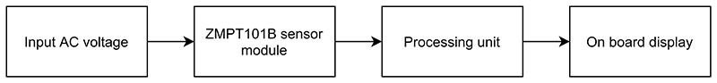
FIGURE 1. System block diagram.
It’s capable of measuring root mean square (RMS) voltage and frequency of the incoming AC sine wave power. The prototype is developed using a ZMPT101B sensor module and LILYGO TTGO T-Display ESP32 Wi-Fi and Bluetooth module development board. The RMS voltage is measured using the ZMPT101B sensor module and the development board is used to process the sensor data and update the same on the onboard display in a graphical format at regular time intervals.
The part I found most interesting is the calibration part, where I compare the inputs and outputs of the ZMPT101B sensor module to arrive at an input-output relation, with amusing revelations. The system uses the official Espressif IoT development framework (ESP-IDF) supported by Espressif for its ESP32 based hardware with up-to-date official APIs for interacting with the hardware.
The framework inherently supports FreeRTOS, which is a real time operating system that enables easy task management, inter-task communication, and real time guarantees for the data shown on the onboard display such that it’s no older than a second from when it’s measured, except the graph part.
This type of software development using FreeRTOS gives a whole new kind of experience compared to the ones that use register level programming for the same application. This was such an adventurous journey, nevertheless well guided by the official documentation provided by Espressif, making it easier to understand and realize the capabilities of their hardware without reinventing the wheel, like interface drivers and RTOS support, which are reasonably reliable.
Hardware Description
The hardware consists of a processing unit with an ESP32-D0WDQ6 chip, an onboard 1.15” IPS display with 240x135 resolution driven by an ST7789V display driver, an ZMPT101B based AC voltage sensor module with signal conditioned output, jumper wires, breadboard, a USB type A male to USB type C male cable, and a female USB type A power port (PC or charging brick) powers the entire prototype.
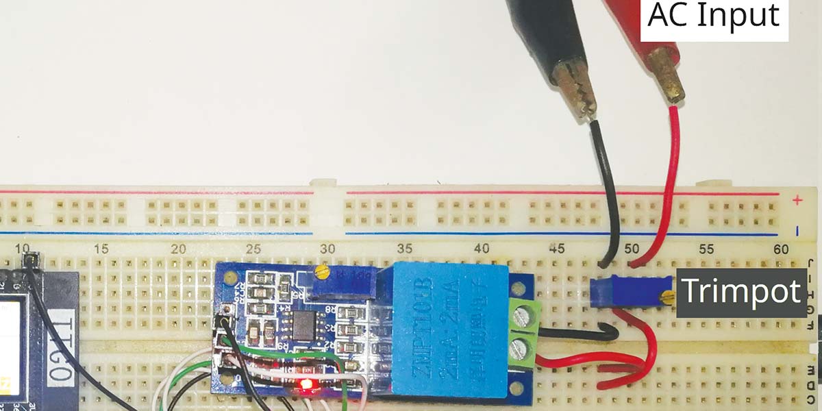
The schematic circuit diagram of the prototype is shown in Figure 2, along with the calibration and testing circuit.
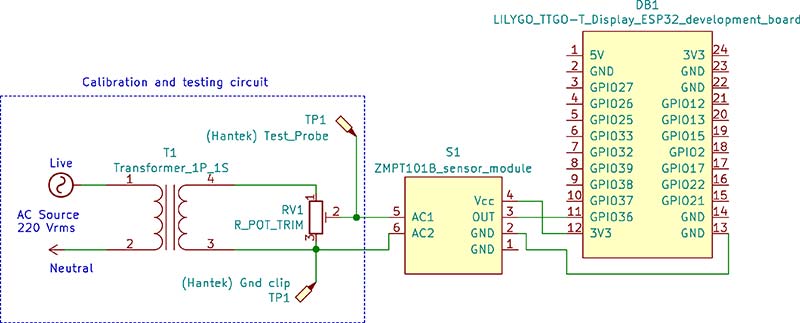
FIGURE 2. Schematic circuit diagram of prototype with calibration and testing circuit.
The entire functional prototype is shown in Figure 3.
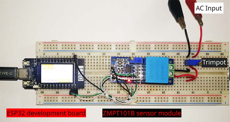
FIGURE 3. Prototype.
Calibration and Testing Circuit
A standard function generator is essential for properly calibrating and making sense of the ZMPT101B sensor module’s output as neither the schematics nor a reliable datasheet for this module were available online.
Due to resource constraints, I had to utilize a step-down transformer with a high voltage (HV) to low voltage (LV) ratio of 10:1 in combination with a 10 KΩ potentiometer to vary the output from the transformer (i.e., input AC voltage to the ZMPT101B sensor module) which is then monitored using a Hantek 6022BL: a PC based USB digital storage oscilloscope (DSO) (see the sidebar). This acts as a custom-built variable amplitude sine wave generator.
During the calibration process, I intended to directly measure the open circuit AC output from the wall outlet using a 100x probe with ground looping in mind. Though I made sure which is live and neutral (live to probe tip, neutral to ground clip), interestingly, the power to the entire room was cut off by my trusty ELCB as the power flowed from neutral to earth through the ground clip of the oscilloscope, causing a wide difference between the current though the live and neutral wire at the ELCB.
I cross-checked this by intentionally shorting the ground to neutral of the AC power outlet using a wire. I’m saving myself and my laptop for another experiment (battery device is perfectly isolated from mains while disconnected from mains, but user still risks electric shock if the metal casing is grounded), as it will be connected to the mains neutral (in our case) through the ground pin of the oscilloscope, which is a problem due to troubling the voltage difference between neutral and ground. It’s enough to shock me and trigger the protection mechanism in the ELCB with 100 mA residual current sensitivity!
The output from this wave generator is given as input to the ZMPT101B sensor module of the prototype for the purposes of calibration and testing through the onboard screw terminal. The transformer was powered using a standard (in India, my home) power outlet with 220V AC at 50 Hz. For generating DC reference voltage, the above said a 10 KΩ potentiometer is coupled with the 3.3 VDC power output from the ESP32 development board and fed to the inputs as required.
In India, the standard household AC voltage has a frequency of 50 Hz. This means this input AC voltage used for calibration and testing purposes is at this constant frequency of ≈50 Hz. According to the Nyquist-Shannon sampling theorem, in order to reconstruct an incoming pure sine wave at 50 Hz, we must sample at greater than 100 Hz (two times the input frequency).
Practically nothing is pure, so it’s recommended to up the sampling rate by five times than that of the frequency of the signal being measured to capture the details. We have upped the sampling rate by almost 10 times in order to make sure we capture the maximum and minimum value with less error possible, without reconstructing the signal and recalculating the maximum and minimum values.
Now, why would one measure a known value? To monitor and detect discrepancies when they happen.
Software Description
The firmware is responsible for initiating and configuring the analog-to-digital converter (ADC) along with its interface, serial peripheral interface (SPI), ST7789V display driver, initiating the tasks, measuring output from the ZMPT101B sensor module, processing the measurements, and displaying the relevant data on the screen. The overall firmware flowchart is shown in Figure 4.
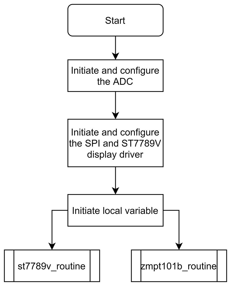
FIGURE 4. Flowchart for overall firmware.
Two different tasks — namely st7789v_routine and zmpt101b_routine — are created in FreeRTOS using the xTaskCreate() function for this particular application. The st7789v_routine task is responsible for waiting until receiving a notification from zmpt101b_routine, copying the inputs from a shared location to local variables after a notification is received, acknowledging the reception of the notification, and displaying the processed inputs on the onboard screen. The flowchart for the st7789v_routine task is shown in Figure 5.
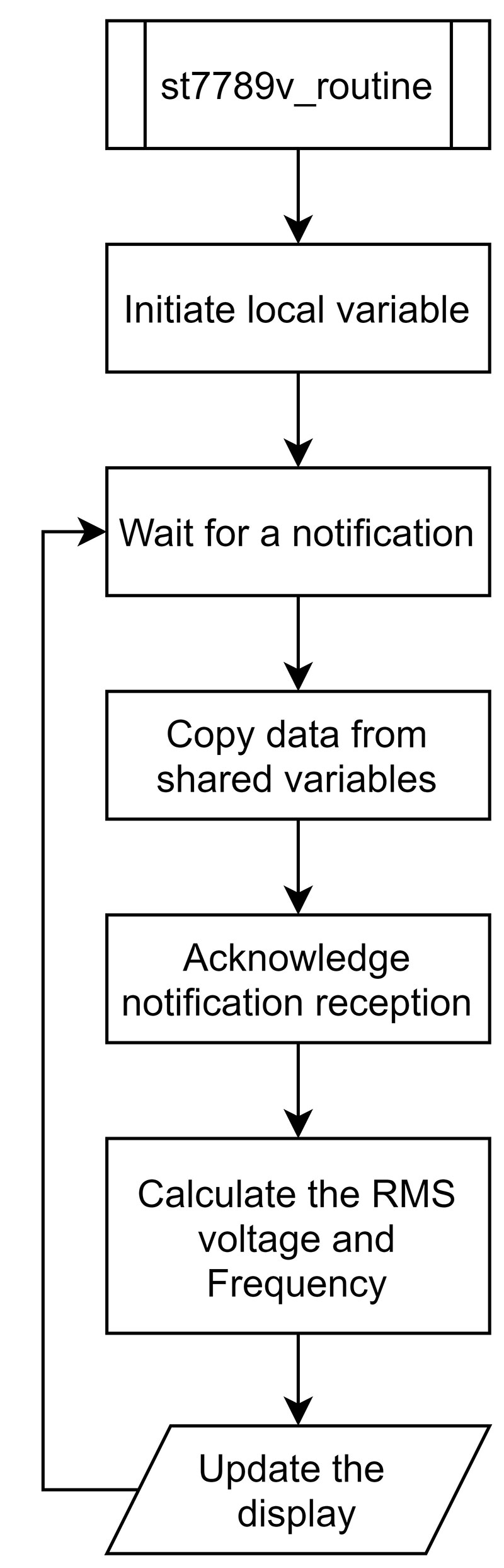
FIGURE 5. Flowchart for st7789v_routine task.
On the other hand, zmpt101b_routine is responsible for collecting the data from the ADC and constantly comparing it with the previous value to find the maximum and minimum values among 500 samples collected at the sampling rate of approximately 1148 Hz (see the sidebar), with each sample being an average of 20 individual ADC outputs themselves, to minimize errors as much as possible.
These maximum and minimum values are converted to millivolts using the onboard ADC reference voltage value stored at BLOCK 0 of eFuse and are used to calculate the RMS voltage of input AC. It also stores the number of samples taken between two zero-crossing events at the ZMPT101B module’s input when it’s rising. This number when multiplied with the sample period of 1/1148 s (≈ 0.871 ms) gives the frequency of the input AC voltage.
This calculation of RMS voltage and frequency happens at st7789v_routine. The data collected by the zmpt101b_routine — namely the maximum voltage, minimum voltage, and the number of samples between respective zero-crossings — are stored in shared variables every 1000 ms. The st7789v_task is notified when new values are available. It keeps notifying the st7789v_task every 100 ms until the st7789v_task acknowledges the reception.
After the acknowledgement is received, the values held by local variables containing the minimum, maximum, and the number of samples between respective zero-crossings are reset and the next sample and update cycle begins. Each sample and update cycle are configured to collect 500 samples within 500 ms and transmit them within the remaining 500 ms. Thus, each sample and update cycle takes 1000 ms or one second. The flowchart for the zmpt101b_routine task is shown in Figure 6.
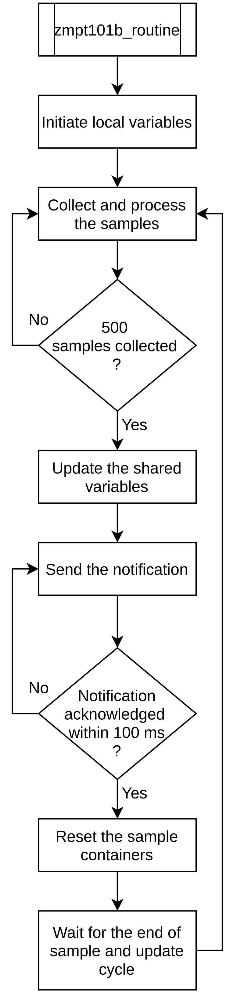
FIGURE 6. Flowchart for zmpt101b_routine task.
The communication of data between these two tasks is facilitated in a synchronized manner using the functions xTaskNotify() and xTaskNotifyWait() and shared variables accessed through pointers. Some of the important system configurations can be found in the file named system_definitions.h in the downloads. The sampling rate is calculated by toggling the GPIO 17 within the super loop of the zmpt101b_routine task and is monitored with a oscilloscope as shown in Figure 7.
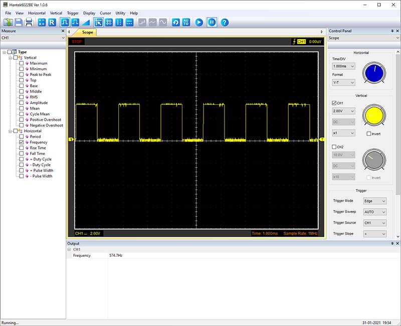
FIGURE 7. Signal from GPIO 17 measured with Hantek DSO.
The oscilloscope then detects the frequency of the square wave signal from this GPIO, which is then multiplied by 2 to get the actual sampling rate. The two tasks mentioned above keep repeating their functions until the power is removed from the ESP32 development board.
Interpreting the Display
When measuring AC voltage input to the ZMPT101B sensor module, the onboard display shows the voltages measured on the top starting with the RMS voltage of the input AC (assumed pure sine wave) on the left, the maximum and minimum voltage measured by the ADC in millivolts from the ZMPT101B sensor module next, and the average of the two on the far right.
The mid section plots the RMS voltage of AC (assumed pure sine wave) measured at regular intervals in the graph such that one pixel on the X axis is equal to one second and the maximum value displayable on the Y axis is given by MAX_RMS_TO_GRAPH macro.
The bottom section displays the frequency of the input AC voltage (assumed pure sine wave). The display of the prototype and its respective sections are shown in Figure 8.
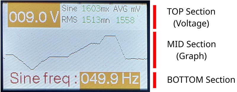
FIGURE 8. Interpreting the display.
When measuring DC voltage input directly to the ADC pin, the average value displayed on the far right of the top section represents the actual input DC voltage as measured by the prototype.
Calibration
To begin with, the ADC unit housed in the ESP32 development board needs to be calibrated. This is done by utilizing the APIs that make use of the ADC reference voltage value stored in BLOCK 0 of eFuse during factory calibration and the pregenerated lookup table representing the ADC characteristics which are then used to generate an esp_adc_cal_characteristics_t struct with initialized member variables. This struct can be passed on to other APIs for converting the 12-bit output from the ADC to millivolts.
If this eFuse doesn’t contain the reference ADC voltage value (like in the ESP32 chips produced way back before the first week of 2018), then the DEFAULT_VREF macro definition is utilized. If the DEFAULT_VREF macro is used, make sure to actually measure the ADC reference voltage in mV by routing it to a GPIO and using a voltmeter to update this macro with the measured value in mV. This process may slightly vary for the latest versions of ESP32 chips like the ESP32-S2.
Since the firmware configures the ADC to attenuate the input signal by 11 dB, the range of input millivolts faithfully measured by the ADC is limited from 150 mV to 2450 mV as it’s the suggested maximum range accurately measurable by the ESP32-D0WDQ6 chip according to Espressif’s official documentation.
In order to verify the accuracy of the voltage reported by the APIs, the 3.3V from the ESP32 development board was used to generate variable DC voltage by connecting it to terminal 1 of the trimmer potentiometer (mid terminal); terminal 2 is connected to the ADC input pin, (i.e., GPIO 36); and terminal 3 is connected to ground as shown back in Figure 2. The DC voltage input to the ADC is varied by rotating the screw on the trimmer potentiometer using a screwdriver.
However, when the actual input voltage reported by the oscilloscope and the measured input voltage reported by the API using the ADC and above calibration settings were tabulated and analyzed, a DC offset error of +100 mV was detected as shown in Table 1.
| I = Actual Input Voltage Measured with Hantek (V) |
M = Measured Input Voltage (V) |
* M-I = Error Voltage (V) |
| 0.15 |
0.2297 |
0.08 |
| 0.50 |
0.5943 |
0.09 |
| 1.00 |
1.0937 |
0.09 |
| 1.50 |
1.6219 |
0.12 |
| 2.00 |
2.1123 |
0.11 |
| 2.45 |
2.5534 |
0.10 |
| |
* Average |
≈ 0.10 |
*Note: Mathematical operations use the rules of significant figures.
TABLE 1. Actual input DC voltage vs. measured input DC voltage by the ADC.
This value is defined in a macro named ADC_DC_OFFSET_mV and used for subtracting the voltage values returned by the official APIs. This DC offset is subject to vary from one device to another and can be adjusted by altering this macro definition.
The ZMPT101B is basically a voltage transformer with electrical isolation from input AC voltage, fitted on a board with unknown schematics containing an LM358 operational amplifier for some kind of signal conditioning. The input and output voltages are related by limiting and sampling resistors attached to the sensor.
Since this value is not properly obtainable due to the lack of a standard datasheet from the vendor (though PCB inspections is another way to obtain this; further error correction might be needed), we assume it’s unknown. Armed with the knowledge/assumption that output is proportional to the input, all we have to do is to find the proportionality constant.
By overall observation, this value was found to be approximately equal to 100 such that when it’s multiplied to the peak-to-peak voltage (PP) calculated by subtracting the minimum from the maximum millivolt observed by the ADC within a sample and update cycle, it gives the RMS input AC voltage in V (PP in mV x 100 = RMS input AC voltage in V).
The difference in AC input voltage measured by the oscilloscope and the prototype can be found in Table 2.
| PP = Peak-to-Peak Output Voltage from Sensor (mV |
Prms = PP x 100, RMS Input AC Voltage Measured by the Prototype (V) |
Orms = RMS Input AC Voltage Measured by the Oscilloscope (V) |
Prms - Orms = Measurement Error (V) |
Error Percentage = |Prms-Orms| x 100
------------------------
Orms |
| 52.5 |
5.25 |
5.00 |
0.25 |
5% |
| 100.6 |
10.06 |
10.00 |
0.06 |
0.6% |
| 146.3 |
14.63 |
15.00 |
-0.37 |
2.5% |
| 198.6 |
19.86 |
20.00 |
-0.14 |
0.7% |
| 245.5 |
24.55 |
25.00 |
-0.45 |
1.8% |
TABLE 2. RMS input AC voltage measured by prototype vs. oscilloscope.
According to Table 2, it could be concluded that the prototype has a maximum error of 5% while measuring input AC voltages within the range of 5V to 25V.
In the final sections, we’ll raise some serious concerns over the validity of this claim and discuss some possible solutions to overcome those concerns.
Firmware Development Environment
The firmware was developed with Visual Studio Code version running on Windows 10 Pro. Before starting the coding and compiling process, you need to set up the environment required for the ESP-IDF tools to operate. This is done by downloading and installing the latest version of Python 3 and Git with the help of a Google search.
While installing both the above tools, make sure to check the appropriate boxes so that the executable paths are added to the environment variable. Download and install the Visual Studio Code (if not already installed) and open it. Head to the extensions marketplace by using the shortcut Ctrl+Shift+X and search for the extension titled ‘Espressif IDF’ by Espressif Systems. Click Install.
Now, use the shortcut Ctrl+Shift+P to open the command palette to search and choose the option ‘ESP-IDF: Configure ESP-IDF extension.’ On the screen, you can see the EXPRESS setup option. Click it. Now choose the appropriate directory (or leave it to default) for the ESP-IDF container and click Install. The setup will download other required tools and install them inside the chosen directory.
Once the setup is completed, the screen will ask you to close the window. The environment is now ready for developing software based on ESP32 hardware.
It’s time to compile and upload the firmware for the target hardware. Import the project folder into Visual Studio Code by clicking ‘Open folder’ under ‘File’ menu. Now click on the small plug-like symbol on the status bar at the bottom of the Visual Studio Code which (on hovering above it) will display the text ‘ESP-IDF Select device port.’
Take a look at the top of the screen to see the list of COM ports displayed. Connect the ESP32 development board to the PC by inserting the USB cable into the respective port. Once again, click on the small plug-like symbol. You’ll find an additional COM port being displayed when compared to the previous one if the connection is done properly. Click on that port to select it. Or, use the device manager to detect the COM port to which the ESP32 development board is attached.
Now click on the small fire symbol on the status bar which (on hovering above it) displays the text ‘ESP-IDF Build, Flash and Monitor’ as shown in Figure 9.
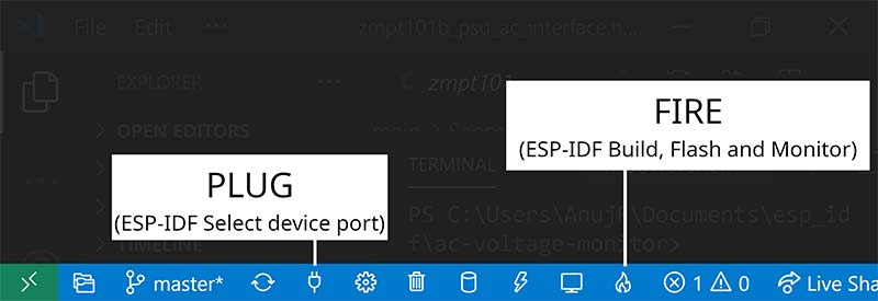
FIGURE 9. Status bar of Visual Studio Code.
This entire process is also described in a quick user guide video at https://github.com/espressif/vscode-esp-idf-extension/#readme.
In case no additional COM port is displayed, head to the device manager and check for the devices attached. If you can find your device, check for yellow warning signs. If the warning sign is present, then this is probably due to the lack of a proper device driver. This particular ESP32 development board uses Silicon Labs’ CP2104 as a USB to UART/TTL bridge. So, install the appropriate driver from the official website at https://www.silabs.com/developers/usb-to-uart-bridge-vcp-drivers#downloads. If you couldn’t find the device, try replacing the cable or try a different USB port.
The ESP32 development board is now ready to execute the target firmware. Once this development board is appropriately connected to the breadboard, the device can be started by pressing the reset button.
These development steps were tested on Visual Studio Code version 1.52.1 with the Espressif-IDF extension version 0.6.1 and ESP-IDF toolset version 4.1.1 running on Windows 10 Pro build 19042 containing Git version 2.30.0.windows.1, Python 3 version 3.9.1 and the CP210x Universal Windows Driver v10.1.10 available in the downloads.
Discussion and Conclusion
I personally feel the measured values (i.e., 500 samples collected per sample) and update cycle are not being utilized to the fullest possible to calculate their RMS value more accurately. However, this also heavily depends on how faithfully the incoming AC voltage is represented by the ZMPT101B sensor module at its output, which is a reasonable cause for concern.
Currently, the sampling rate is a random constant, auto set by the time period of execution of codes within the super loop of zmpt101b_routine. Though this time period is fairly constant due to the very low clock period of the processing unit combined with very low unpredictability and fairly constant branching of instructions, it’s not the safest method to achieve a constant sampling rate in the ADC as the future updates to the code might change this value.
One of the proper ways to achieve a constant sampling rate is to use the built-in hardware support from ESP32 like timers since this ensures the sampling rate is independent of the instruction execution time by the processing unit, which might vary depending on the state of the processor like the instructions in the pipeline, branch predictor state, cache state, and so on. Another way specific to the ESP32 might be to configure the ADC itself and use it in DMA mode, which seems to provide some kind of control over the sampling rate of the ADC that I haven’t explored yet.
Another way is to store the TWO POINT values in BLOCK 3 of eFuse, which is later used for increasing the accuracy of the voltage measured by the ESP32’s ADC. The TWO POINT values are the raw values of the ADC at 150 mV and 850 mV as measured by the user.
One should also consider the characteristics of the actual ADC hardware used as the increase in value of parameters like non-linearity error requires user side lookup table creations, which then might be used for generating higher order ADC characteristic equations to improve the accuracy. Or, one could choose better ADC hardware whenever the application allows or requires.
The output from the transformer in the calibration and testing circuit should be regulated or the entire circuit must be replaced with a function generator for generating reliable reference AC voltage which can then be used for calibrating the sensor and also to increase the accuracy and precision of the readings utilized for testing.
Another important thing to note is the max possible input AC voltage measured by the ZPT101B sensor module. Figure 10 shows how the voltage output from the sensor module is chopped while the input AC voltage is 220V.
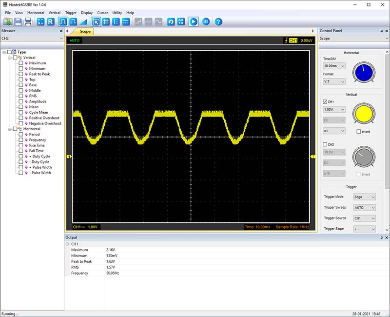
FIGURE 10. Chopped output from ZMPT101B sensor module measured using Hantek.
This might be due to the output voltage swing to positive rail limitations in LM358 op-amps as the sensor module is powered by the ESP32 development board at 3.3V. Increasing this powering voltage while staying within the recommended operating conditions might alleviate this issue.
Despite all these shortcomings, I was surprised to find that the frequency measured by the prototype stayed mostly at 49.9 Hz, which is close to the standard AC power output specification of 50 Hz in India and equal to what’s measured by Micro Power Monitor GM86, which directly plugs into the AC power outlet for monitoring the AC power characteristics as shown in Figure 11, in which the frequency of AC voltage from the outlet is being displayed as 49.96 Hz.
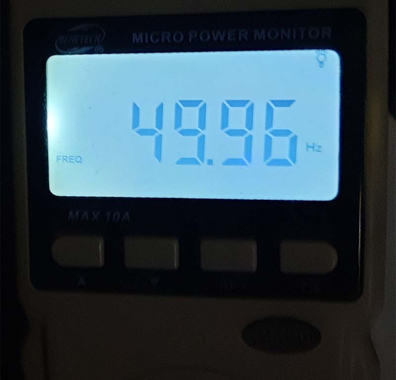
FIGURE 11. Frequency of AC input displayed by Micro Power Monitor GM86.
Apart from the sampling rate issues, the small difference in value can also be blamed on the quantization error as a fall in value by one LSB of the measurement — number of samples collected between two successive zero-crossings at the ZMPT101B sensor module’s input — when the input is rising can increase the frequency from 49.9 Hz to 52.2 Hz. This accuracy in frequency measured can be attributed to the characteristics of FreeRTOS. NV
Parts List
ZMPT101B Sensor Module
LILYGO TTGO T-Display ESP32 Wi-Fi and Bluetooth Module
10K Potentiometer
Single-phase Step-down Transformer (10:1 primary vs. secondary coil turns ratio)
AC Power Source
Miscellaneous
Breadboard
Jumper Wires
Crocodile Clips
Connecting Wires (single-stranded and multi-stranded)
Wire Insulation Strippers
Crimping Tool
For Calibration
Hantek 6022BL Oscilloscope
Laptop (for interfacing the oscilloscope)
Resources
I thank Dr. K. Vairamani for investing his time and effort in reviewing and formatting this article before submission.
Downloads
What’s In The Zip?
Code
Schematic