Sometimes called a VI curve tracer, an IV curve tracer, or an oscilloscope Octopus, this general-purpose instrument is invaluable in troubleshooting (Figure 1). The Octopus generates AC excitation across its two leads and then displays a voltage vs. current plot in real time. The resulting plot can be used to track down opens, shorts, and noise in a component, as well as measure the breakdown voltage and phase relationship between voltage and current. The circuit has been around just as long as oscilloscopes, but this Octopus is a small battery-operated instrument with its own display. Instead of an octopus’ worth of jumbled cables, there’s now just a pair of test leads.
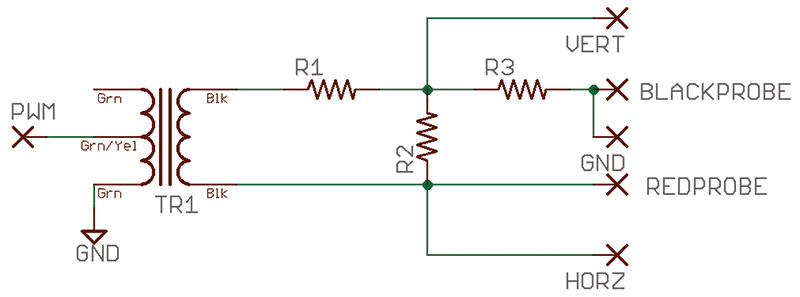
FIGURE 1. Classic Octopus.
Principle of Operation
The Octopus (Figure 2) applies a 15 volt peak 60 Hz sine wave across the two test terminals. The current through the device under test (DUT) and the voltage across the DUT is measured and then displayed on the screen. The excitation is current-limited for protection of the DUT. The resulting cartesian plot has voltage on the X axis and current on the Y axis.
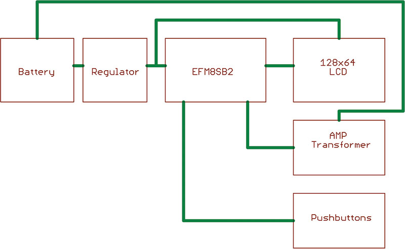
FIGURE 2. Overview.
Circuit
Overview
The circuit only has a few tasks to perform: generate excitation; measure the signal; and then display the results. A Silicon Labs EF8SB20 generates the signal, measures the signal, and then plots the results on a Newhaven 128x64 LCD. Current draw is important in battery applications, so the microcontroller powers off into a sleep mode after several seconds of inactivity.
Excitation is a 15 volt peak sine wave that is generated by the microcontroller’s pulse width modulation (PWM), filtered, bridge amplified for extra current drive, and then stepped up through a line transformer.
The LCD display is written through a parallel interface which produces a very satisfactory frame rate. Although the LCD does feature a low current sleep mode, this design turns the LCD power on or off. The purpose of power cycling the display is to protect the design from firmware crashes of the LCD that might require a cumbersome battery removal.
By power cycling the display, it will also be reset each time the microcontroller wakes up. Either method could have been used, but I considered this a little more robust.
Microcontroller
The EFM8SB20 is Silicon Labs larger version of their Sleepy Bee family of processors. The micro is based on the time-honored, eight-bit 8051 core with pipelined improvements in speed and memory access.
PWM
The processor has a full peripheral suite which helps to make this product easy to design. The first important peripheral is the programmable counter array (PCA), which can be configured for a wide variety of tasks. This design uses the PCA to generate a PWM whose value changes on a regular basis to approximate a sine wave. A separate timer is programmed to trigger at 960 Hz, which is 60 Hz * 16.
Each interrupt service routine (ISR) loads a different PWM value into the PCA. Sort of a by-product of the PCA, the PCA base clock is also used as a general-purpose timer. Refer to Figure 3.
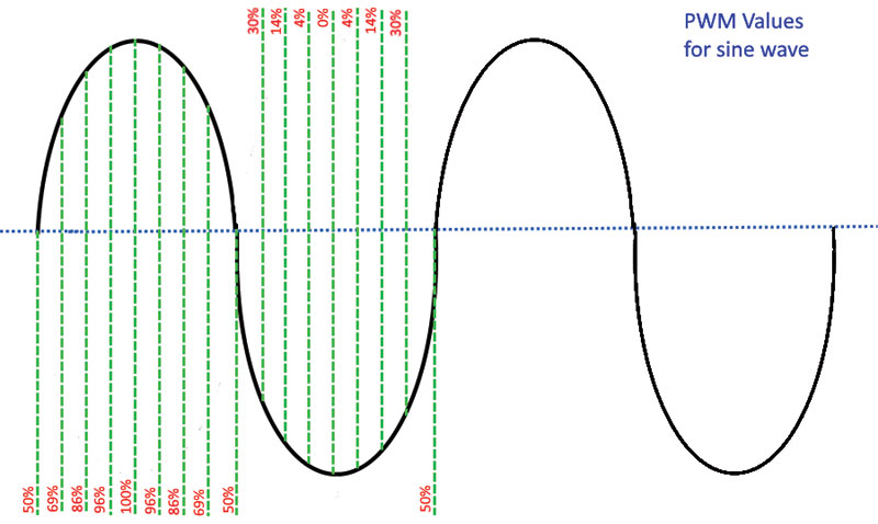
FIGURE 3. Sine generation.
ADC
The analog-to-digital converter (ADC) in the processor supports speeds up to 300 ksps and a resolution of 10 bits, which is more than adequate for this project. The design will require two channels of conversion: one for the X axis at a resolution of 128; and a second for the Y axis with a resolution of 64.
In order to obtain a resolution of 128 pixels at 60 Hz, the two channels will need to be read every 130 µs. A separate timer is programmed to trigger each of the 130 µs intervals.
Sleep Mode
After several seconds of inactivity, the display will turn off and the processor will enter a sleep mode, which holds the current draw to about 2 µA.
The Sleepy Bee — as the name implies — has several different types of sleep modes and methods to wake up from them. This project uses the real time clock (RTC) to wake from the sleep mode and poll the pushbuttons. Using the RTC for waking also has some benefits for debugging; more on that later.
Transformer/Audio Amp
With only three volts available, there needs to be some method of stepping the supply up to the 15V peak needed for excitation. So, 60 Hz was chosen as an excitation frequency as a good compromise between processor performance and component availability.
A 60 Hz line transformer is cheap, widely available, and performs flawlessly at low frequency. Yes, it’s heavy and bulky for the power required, but it performs well at a very low price (Figure 4).
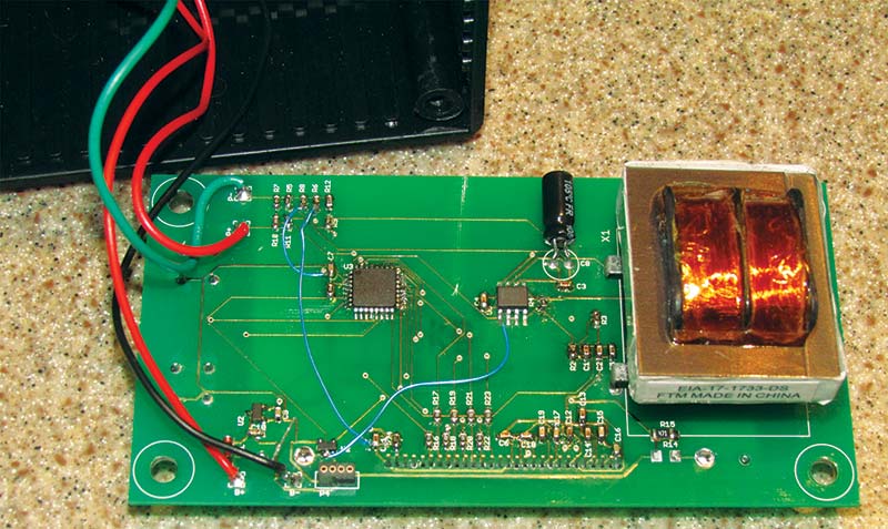
FIGURE 4. Component side.
In order to be driven properly, the transformer requires a linear drive with a fair amount of current. Several amplifiers or transistor arrangements would work well, but an off-the-shelf monolithic audio amplifier is designed to provide exactly the performance at the frequency needed.
As a bonus, the amplifier operates in bridged mode for a higher voltage drive. ON Semiconductor’s NCS2211 was chosen for its cost, performance, and the extra benefit of a shutdown pin for the sleep mode.
LCD
The display is Newhaven’s NHD-C12864LZ, 128x64 backlit LCD. A few other displays were considered and prototyped for the design, but the Newhaven was chosen for its proper size at the right resolution; 128 bits of horizontal resolution is pretty much the limit of the processor while running with a 60 Hz excitation. The case needs to be large enough to house the battery pack and transformer, so the larger size of Newhaven’s display is a nice aesthetic choice for the case.
Schematic
The circuit is designed to run from four AA batteries. Power enters at wire pads B+ and B-, with polarity protection provided by diode D1. Unregulated supply voltage is provided for the audio amp and the LCD backlight, while regulator U1 provides 3.3 VDC for the microcontroller and LCD. Refer to Figure 5.
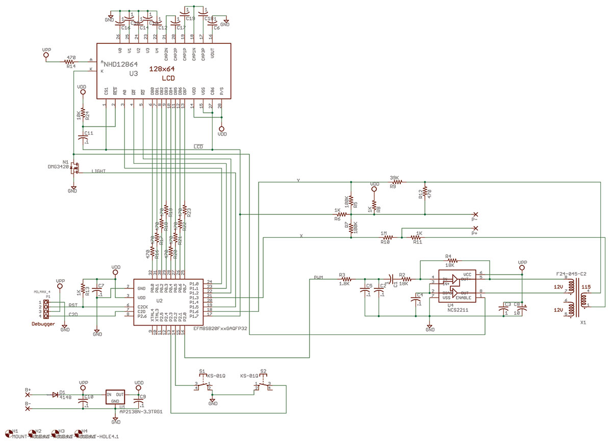
FIGURE 5. Schematic.
Microcontroller U2 does all the work; its debug interface is P1 and R13. Check out the schematic. Resistors R16–R23 are in series with the data bus to the LCD display. The purpose of these resistors is to prevent damage to the microcontroller from an inadvertent bus contention. The bus is bidirectional, and if both the LCD and micro should try to control the bus at the same time, the micro will be damaged.
This shouldn’t happen under normal circumstances, but it did happen during development, so the resistors were added.
The parallel interface to the LCD also consists of address line A0, read enable RD, and write enable WR. Active low power is provided to the display on port pin P1.7. This pin has a shared duty with the voltage divider at R6. PWM output is provided at pin P2.0. The ADC inputs are at P1.3 and P1.6.
LCD U3 has an array of capacitors (C12–C18) that is used with a charge pump to boost the bias voltage of the LCD. R24 and C11 provide a ramp delay for the LCD reset pin. R14 is the current limiter for the LCD backlight. The backlight is capable of handling up to 100 mA of current, but this design only allows about 6 mA to flow through the backlight.
The display is quite readable with 6 mA; more current just means less battery life. If you wish to have a brighter display, you can change R14 to a lower value. R15 is in parallel with R14 for increased dissipation if you want the display to be very bright. N1 is an N-channel MOSFET that turns on the backlight. It also has a shared duty to provide the sleep signal to U4, the audio amplifier.
Pushbuttons S1 and S2 provide user input to wake the unit up and move the graticule left or right. You could get the job done with one button, but two are available to provide easy expansion for additional user features.
Audio amplifier U4 accepts signal from the microcontroller’s PWM, which is filtered through R2, R3, C1, C2, and C5. R2 and R4 set the voltage gain of the audio amplifier, but in this application, only current gain is needed.
The audio amplifier’s supply is directly from the batteries, which protects the voltage regulator from unnecessary dissipation.
The output of the amplifier is bridged, which yields a voltage gain of close to one. This is stepped up through transformer X1, which provides DC isolation and a 30VPP excitation.
Enable line pin 1 is connected to the backlight cathode. This seems a little odd, which suggests that there must be a good reason for the odd connection, and there is. The amplifier is supplied by the unregulated 6V supply, so the shutdown logic level needs to be 0-6V.
The microcontroller runs off the regulated 3.3V supply and would not provide a high enough logic level to prevent excessive bias current to flow through the enable pin. By using the backlight as a pull-up device, the enable pin will see a hard 6V to 0V transition. This will keep the sleep current below 1 µA.
Resistors R6-R12 provide current limiting for the excitation. Resistors R6 and R8 provide the 1/2VDD reference for the ADC. This reference is turned on and off through the active low LCD power pin. The transformer’s output is held to the reference through R12. R5 and R9 form a voltage divider for the Y ADC input, while R10 and R11 are the voltage divider for the X input.
Software
With all the peripherals in the Sleepy Bee, there’s very little software work to be done. Even with the startup graphic, the project requires just over 2K of code. There are six software modules used for the Octopus, with a description of each below.
InitDevice.c
This module is generated by Silicon Labs’ Configurator. The Configurator is an add-on built into Simplicity Studio. The Configurator allows the developer to configure the peripherals of the micro through a graphical interface, rather than pouring over a user manual trying to figure out how to configure the PCA for just the right PWM.
The Configurator may have several different modes of operation. As an example, in this project, we have default and sleep. Once all the peripherals are configured, the Configurator will auto-generate the file InitDevice.C, as well as the header InitDevice.h.
Peripherals used are ADC0, clock control, interrupts, PCA channel 0, RTC, voltage reference, Timer1, and Timer2.
IO.c
This file — along with IO.h — contains the definition and low level functions for the peripherals. Function IOWaitUs waits x microseconds by polling the PCA counter for the time to pass. There is certainly overhead in calling IOWaitUs, so a 5 µs delay may work out to actually being 8 µs, but this is close enough for most software functions. IOWait waits x milliseconds by calling IOWaitUs with an argument of 1000.
Sine_ISR is the ISR for Timer2. This timer runs at 960 Hz, which is 60 Hz * 16. At each of the 16 intervals, the PWM rate will be set for the next value of the sine wave.
IOLCDOn sets the LCD data bus high. The reason is that the LCD power is active low, so when the LCD is turned off, it will float high. If the data bus is low, then excessive current will flow through the data bus into the LCD. This will negatively impact the sleep current.
Keyboard.c
The keyboard is debounced through this module, and this is a module that I use in all my projects. The module has the ability to make a key repeat if it’s held down, and repeat (slew) faster if the key is held down for a longer period (Figure 6).

FIGURE 6. Keyboard debounce.
LCD.c
This module is the only one that has any complexity, as you would expect when it comes time to juggle graphics. The complexity could have been dispensed with by omitting the splash screen, but the splash screen adds to the look of the project and the code is nice to have for the next project.
LCDExtractRLE is a private function for decompressing a run length encoded bitmap. Most bitmaps — especially line graphics — have huge amounts of white space and other repeated data. The RLE format has a signed count byte that designates how many times the data byte will be repeated, or how many bytes of raw data will follow.
Using our Octopus as an example, the Octopus.h file shows 0x0c, 0x00, meaning that the byte 0x00 is repeated 12 times. The next count byte is 0xf3, since the count byte is signed. 0xf3 is a negative 13; this means there will be 13 bytes of raw data to follow (Figure 7).
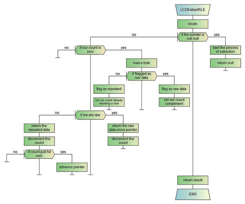
FIGURE 7. LCDExtractRLE.
The function has a single argument. If the argument is not null, the argument points to the location of the RLE file to decompress. If the argument is null, the function will continue decompressing the current file.
LCDWriteRLE is a public function for writing an RLE bitmap to the screen. The function has an argument for the X and Y position of the bitmap and a third argument for a pointer to the bitmap. Notice the modifier “code” in the argument list. The Keil compiler used by Simplicity Studio has an extension for designating what type of memory a pointer is pointing to. You don’t have to use the memory designator, but the code size is smaller and it executes faster if you do.
The LCDs memory is arranged as 128 columns x 8 rows, where each row contains data for eight individual lines; one for each bit in the row’s byte. Frame buffers have been arranged this way since the early days of computing, and as annoying as it is, we’ve gotten used to it.
From a historical point of view, this was a great arrangement when you had a character font that was eight pixels tall, but it makes for a bunch of bit juggling when you attempt to place a bitmap. In this display, column 0, line 0 is bit 0 of the first byte. Refer to Figure 8.
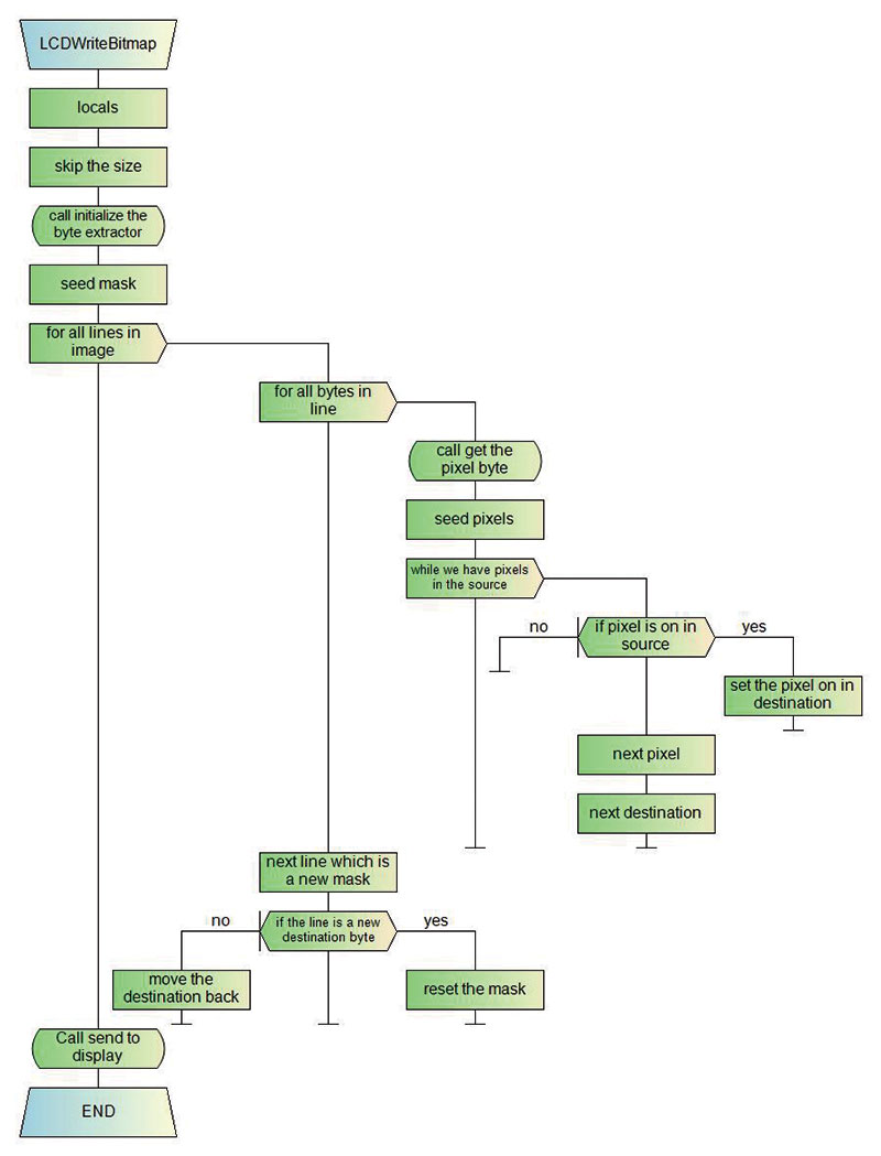
FIGURE 8. LCDWriteBitmap.
After determining the width and height of the bitmap, the function has two for loops for the width and height. LCDExtractRLE is repeatedly called to fetch a byte of the bitmap, and that byte is shifted down the appropriate number of bits required for the Y placement of the graphic. Note that the variable bitmap is a union. This allows the software to shift the byte of data through a four-byte long without having to worry about the carry bits.
LCDInit is a public function for setting the display driver to operate with the display glass. These values come from the Newhaven’s specifications. The contrast value may be tailored to your taste.
The other functions are very straightforward for moving the pins properly in order to talk on the data bus, as well as primitives for setting the page and column.
Plot.c
This performs the actual plotting of the signal on the display. The display is plotted by first performing 128 ADC measurements spaced evenly across the 60 Hz excitation. That’s measuring two channels and plotting the result every 130 µs, so it has to run fairly fast. It’s not possible to send the data to the display at that speed, so all 128 readings are plotted first and when complete, that result is sent to the display.
The time spent sending the screen data to the display isn’t critical to the accuracy of the measurement. So, when the write is complete, the next measurement sequence can be started at any time. If 128 measurements are completed at the proper time, it doesn’t matter when the sequence started.
This display has a fairly slow response time, which would make for cumbersome measurements if each measurement sequence had to pause for the display to reach full brightness. Rather than waiting, the software adds some persistence to the display, so that old measurement sequences are not erased when new ones are drawn. Instead, the erase only occurs every so often, which is every fifth time in this example. This method results in a high contrast display and a quick frame rate.
PlotScale is a private function that draws the graticule on the display. Although a for loop would have worked well and been more readable, the code is written in-line for speed. The variable mark is used to move the graticule across the display if it isn’t properly centered when the probes are shorted. You may want to customize this function for your own graticule.
Plot is the public function that starts the measurement sequence. At entry, Plot will position the graticule and then determine if the screen persistence requires the frame buffer to be cleared. Timer0 is programmed for a 130 µs period.
The for loop makes 128 pairs of measurements by first waiting for Timer0 to expire and then reading the X channel and then the Y channel. The Y channel reading has a delay of 10 µs for settling the ADC MUX. The X channel does not include this wait period because the end of the loop sets the MUX for the X channel when the loop is complete, so it’s not necessary to wait any additional time.
Octopus_main.c
A portion of this module is generated by the Configurator. There are precautions in the file about not placing any of your own code between the bracketed comments. This is because the Configurator places its own code inside those bracketed comments and leaves the code outside of the brackets (your code) alone.
The first function call sets all the peripherals to the Default Mode. After this call, the PWM is running as well as all the timers. The next calls start up the interrupts, initialize the display, and turn on the backlight. At this point, the Octopus is drawn for the splash screen. After a few seconds, the screen is cleared before entering the Main Loop.
The Main Loop maintains sleepTimer, which is a counter that prevents the unit from sleeping when it’s non-zero. If the timer should count down to zero, the display is turned off by first setting the data bus to 0xFF, turning off the display, and then setting the peripherals for the Sleep Mode. There is a conditional for DEBUG at this point. If you’re debugging the device, you don’t want it to go to sleep because that will crash the debugger. So, this switch will have the unit simply pause for 100 ms, rather than actually going to sleep.
If the unit does go to sleep, please note the sequence involved in invoking sleep on a Silicon Labs part. Not following the sequence can brick your part or make it very unstable when it wakes up. The precaution to follow is to disable interrupts, clear the Power Mode flags, and then set the Power Mode flags.
At this point, the part is asleep. The next NOPs flush the pipeline after the part awakes and then you can turn on the interrupts.
If the unit didn’t go to sleep, the keyboard is debounced and the signal is plotted. This loop is run as fast as it can go, so the keyboard debouncing is not exactly as stated in the Keyboard Module.
Sample Displays
Open
With the simplest trace — which is also the default trace — from -15V to +15V, the current remains 0 (Figure 9).
FIGURE 9. Open circuit.
Forward/Reverse Bias
The Octopus is useful in determining if a device conducts in forward, reverse, or both directions. With this, you can determine component polarity or damage. A device that breaks down in the forward direction will display zero current in the negative voltage and then suddenly display positive current with positive voltage (Figure 10).
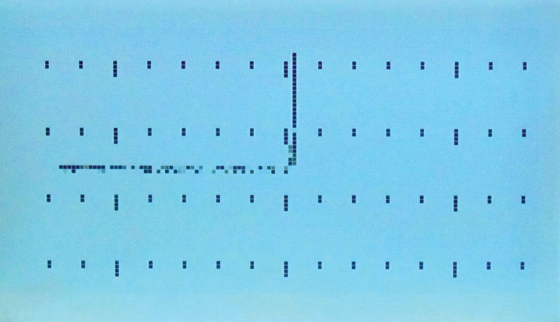
FIGURE 10. Forward bias.
Reverse bias is just the opposite, displaying high negative current with negative voltage and no current with positive voltage. Some devices such as transistor base emitter junctions will display breakdown in both directions (Figure 11).
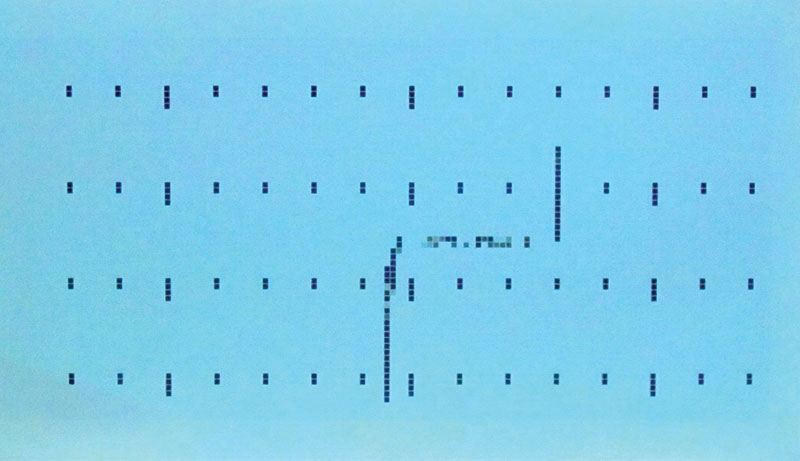
FIGURE 11. Base/emitter junction.
Breakdown Voltage
Probably the most useful feature of the Octopus is determining a device’s breakdown voltage. A graticule on the Octopus is scaled with 2V minor ticks and 10V major ticks.
Reactive Devices
Because a reactive device has voltage and current out of phase, a reactive device will display an ellipse (Figure 12) if the reactance is within range of the Octopus’s display. This is a .1 µF capacitor.
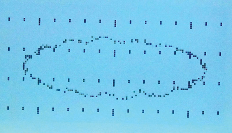
FIGURE 12. A .1 µF capacitor.
In-Circuit Troubleshooting
A great advantage to this type of tester is that the component being tested does not have to be removed from the circuit. Just remember that these tests must be performed with the power off.
One troubleshooting technique is to use signature analysis, where the errant board is compared to a good board. Place the black probe on the test circuit’s ground, and then probe around at each suspect node to see if the suspect node matches the same node on the good board.
Construction
Prior to building the board, you may want to use the blank board as a drilling guide. The project was designed to fit in a Hammond 1591T enclosure (www.hammondmfg.com) using a clear plastic cover. To drill the cover, position the blank printed circuit board (PCB) between the cover bosses and drill the mounting holes. Screw the cover to the lid and then drill the center position for the two switches.
The pitch on all the components is large enough to permit hand soldering. Of course, if you have an oven or a heat gun, that’s the way to go. Solder all the surface-mount parts first. The microcontroller should be programmed at this time, using the debug connector to supply power to the board. The code size is small enough that any of the 32-pin QFP parts in the EFM8SB2 family may be used.
If you build the project yourself, rather than using the hex file, make certain to build the Release version, since this will put the unit to sleep and keep the current draw down to a couple of microamps.
Install the transformer to the component side of the board and trim the two primary leads as close as possible to the board or trim them prior to mounting the transformer. These leads are under the display, so you don’t want them to poke up into the backlight area.
Carefully mount the LCD and switches to the back side of the board. Note that the notches on the switches should be at the top of the board. Add wires for the probe and attach the battery holder.
Testing
If you have a current-limiting power supply, you should use that to test the board first before installing batteries. The unit only pulls about 25 mA, so limiting the supply to 100 mA will provide plenty of current and prevent any mishaps.
After power-up, the unit should display the splash screen for a few seconds and then begin displaying the measurement screen. After about a minute of no signal (meaning with the probes open), the unit should enter the sleep mode and the current should drop to a couple of microamps.
Modifications
Hardware
Adjusting R11 and R12 will provide different Y gain for different current, which needs to be balanced with changing R9 for full scale. Adjusting R4 will provide different excitation voltage which will have to be balanced with adjusting R10 for full scale.
The backlight brightness can be adjusted by changing R14, but remember that more current means a shorter battery life and dissipation by R14.
Firmware
There are two pushbuttons, and the design can really get by with just one, so additional features can be added by changing how the buttons operate. Additional ranges could be added by changing the PWM output and adjusting the gain of the ADC.
The display timeout can be easily changed by changing the value of SLEEP_TIMER in Octopus_main.c. The graticule can be modified by changing the plotting routine in PlotScale, located in Plot.c.
You can also experiment with different levels of persistence by changing the value of PERSISTANCE, also in Plot.c.
Conclusion
This Octopus is a great addition to your workbench. It’s small, battery operated, and doesn’t have eight leads dangling off of it as it ties up your oscilloscope.
Also, the display functions are a handy addition to your next graphic display project. Hopefully, you’ve had a chance to kick the tires on Silicon Labs Sleepy Bee. NV
Resources
Silicon Labs
www.silabs.com
Newhaven Display 128x64 COG
www.newhavendisplay.com/nhdc12864lzfswfbw3v3-p-4161.html
Run-length Encoding
https://en.wikipedia.org/wiki/Run-length_encoding
Code Rocket Designer
www.rapidqualitysystems.com/Products/CodeRocketDesigner
Parts List
| Qty |
Value |
Device |
Parts |
| 7 |
0.1 |
C-USC0603 |
C2, C4, C5, C7, C9, C10, C11 |
| 11 |
1 |
C-USC0603 |
C1, C3, C6, C12, C13, C14, C15, C16, C17, C18, C19 |
| 1 |
1.8K |
R-US_R0603 |
R3 |
| 4 |
1K |
R-US_R0603 |
R6, R8, R11, R13 |
| 1 |
1M |
R-US_R0603 |
R10 |
| 1 |
10 |
CPOL-USE2,5-6E |
C8 |
| 1 |
10K |
R-US_R0603 |
R24 |
| 2 |
18K |
R-US_R0603 |
R2, R4 |
| 1 |
39K |
R-US_R0603 |
R9 |
| 2 |
100K |
R-US_R0603 |
R5, R7 |
| 10 |
470 |
R-US_R0603 |
R12, R14, R16, R17, R18, R19, R20, R21, R22, R23 |
| 1 |
4148 |
DIODE-SOD80C |
D1 |
| 1 |
AP2138N-3.3TRG1 |
LDOSOT23 |
U1 |
| 1 |
DMG3420 |
NMOSSOT23 |
N1 |
| 1 |
EFM8SB20FxxGAQFP32 |
EFM8SB20QFP20 |
U2 |
| 1 |
F24-045-C2 |
XFRMR_DUAL_SEC |
X1 |
| 2 |
KS-01Q |
DT6 |
S1, S2 |
| 1 |
NCS2211 |
NCS2211 |
U4 |
| 1 |
NHD12864 |
NHD12864 |
U3 |
Downloads
What’s in the zip?
Code Files
Schematic Files
CAD File