This article is focused on learning how a microcontroller core is designed, and is intended for educational use only. Please visit www.zilog.com and check the manufacturer product line to select a microcontroller that fits your project needs (from eight-bit Z8 Encores! and eZ80 Acclaims to the 32-bit ARM Cortex-M3 based ZNEO32! which includes advanced motor control capabilities).
My love affair with microcontrollers and microprocessors began back in 1988 when I was working toward a technical degree at CEFET-PR (a four year Brazilian secondary/technical school and university located in Curitiba). I began by learning the basics while exploring the classic Zilog Z-80 (Figure 1a).
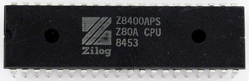
FIGURE 1A. The Zilog Z-80A (courtesy of Wikimedia Commons).
Fast forward through a career of programming that included authoring some books on microcontroller programming (see Resources), starting a small design house (ScTec), and finishing a post-graduation program at CEFET-SC (another Brazilian university located in Florianopolis). This was in 2008, when I had more contact with programmable logic and VHDL and my curiosity was peaked. Years later in 2016, I found a very affordable FPGA (Field-Programmable Gate Array) kit and decided to give it a chance, and started learning more about FPGA technology.
What would be better than designing a softcore to learn more about VHDL (VHSIC hardware description language), FPGAs, and microprocessor cores themselves? I ended up choosing a modern Z-80 relative: the Zilog Z8 Encore! (a.k.a., eZ8; Figure 1b).
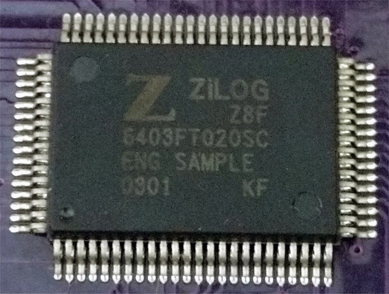
FIGURE 1B. Zilog eZ8.
It’s an eight-bit microcontroller core with a simple — yet powerful — instruction set and a very nice on-chip debugger. With its lightweight IDE (integrated development environment) and free ANSI C compiler, it is an excellent project to learn (and also teach) about embedded systems.
Before diving into the depths of the core operation, VHDL, and FPGAs, let’s take a glance on the Zilog Z8 Encore! features.
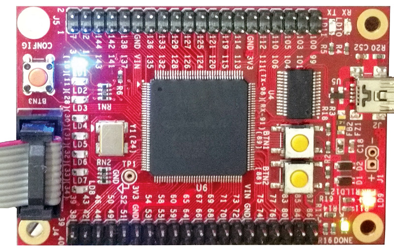
FIGURE 1C. FPz8 on an FPGA.
Zilog Z8 Encore!
The eZ8 is an eight-bit microcontroller family based on Zilog’s successful Z8 family and on the great Z-80 heritage. It features a Harvard CISC machine with up to 4,096 bytes of RAM (file register and special function registers area), up to 64 KB of program memory (usually Flash memory), and up to 64 KB of data memory (RAM). The eZ8 core also includes a vectored interrupt controller with programmable priority and an on-chip debugger which communicates with the host computer using asynchronous serial communication. These microcontrollers are packed with a very nice peripheral set, ranging from versatile 16-bit timers to motor control timers, from multiple UARTs (IrDA ready) to USB devices, and much more (visit www.zilog.com to check the full product line).
One major feature of the eZ8 programming model is the lack of a fixed accumulator. Instead, any of the 4,096 possible RAM addresses can work as accumulators. The CPU treats its main RAM (the file and SFRs — special function registers — area) as a big set of CPU registers. In order to accomplish that, RAM is split into register groups (there are 256 groups of 16 working registers each). An instruction usually works within a single working register group, which is selected by an SFR named RP (register pointer). Note that all SFRs are located at the last page of RAM (addresses starting from 0xF00 up to 0xFFF).
Regarding the instruction set, there are 83 different instructions split into two opcode pages. It comprises usual instructions for basic operations such as addition, subtraction, logical operations, data manipulation instructions, shifting instructions, change-of-flow instructions, some 16-bit instructions, bit testing and manipulation, 8x8 multiply, etc.
The program memory area is organized so that the first addresses are dedicated to special purposes. Addresses 0x0000 and 0x0001 are dedicated to the configuration options; addresses 0x0002 and 0x0003 store the reset vector; and so on. Table 1 shows program memory organization.
| 0x0000 |
Option bytes |
| 0x0002 |
Reset vector |
| 0x0004 |
WDT vector |
| 0x0006 |
Illegal instruction vector |
| 0x0008 to 0x0037 |
Interrupt vectors |
| 0x0038 to 0xFFFF |
User program memory area |
TABLE 1. Simplified program memory organization.
Some devices also include a second data space (up to 65,536 addresses) which can only be accessed by using LDE/LDEI instructions. This area can be used to store less used data (as reading/writing to it is slower than the RAM/SFR area).
FPz8
The first implementation of FPz8 uses a very conservative and hardwired design approach with two main buses: one for program memory, and another for register memory. As I chose not to include a data memory area, the LDE/LDEI instructions are not implemented.
The program memory buses comprise a 16-bit instruction address bus (IAB), an eight-bit instruction data bus (IDB for reading data from program memory), an eight-bit instruction write data bus (IWDB for writing data to program memory), and a PGM_WR signal which controls writing to program memory. FPz8 includes 16,384 bytes of program memory implemented using synchronous block RAM (which means program memory content is lost when the device is powered down).
The five register area buses comprise three for the file register area (user RAM), and another two dedicated to special function registers. There is a main 12-bit file register address bus (FRAB), an eight-bit file register input data bus (FRIDB), an eight-bit file register output data bus (FRODB), an eight-bit register input data bus (RIDB), and finally an eight-bit register output data bus (RODB) for writing into SFRs. The FPz8 includes 2,048 bytes of user RAM memory implemented using synchronous block RAM.
Figure 2 shows a block diagram of the FPz8; you can see the CPU, two memory units (one for program storage and the other for data storage), and also an external timer module.
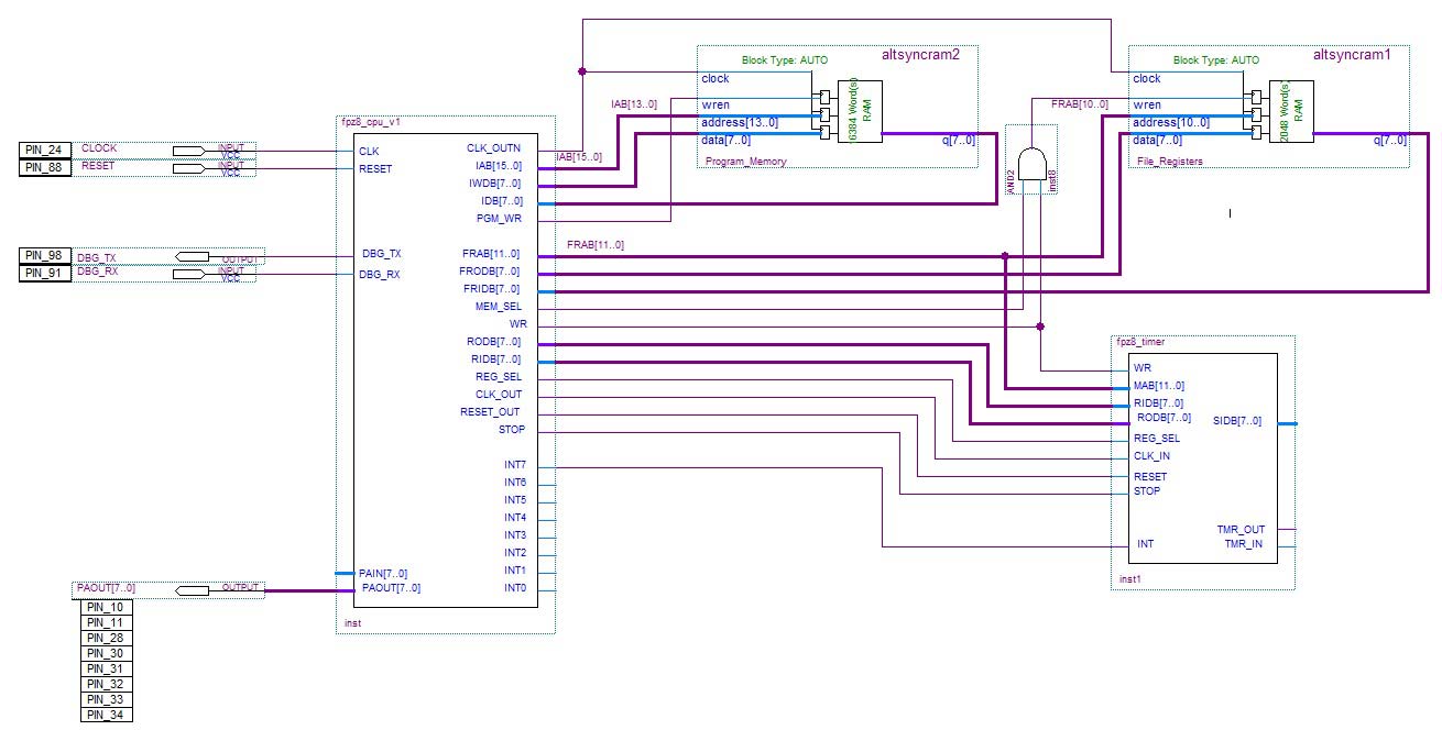
FIGURE 2. FPz8 block diagram.
Note that I am not using bidirectional buses for any interconnects in this project. Unidirectional buses are simpler to use, although they are less space efficient.
The VHDL description of the FPz8 is large and a bit complex, so I am going to split its operation into some modules to ease comprehension:
- Instruction queueing engine
- Instruction decoding
- Interrupt processing
- Debugger
Instruction Queueing Engine
Fetching instructions is a primary task for any CPU. The FPz8’s Harvard architecture enables concurrent fetching and data access (due to separate buses for instruction and data). That means the CPU can fetch a new instruction while another is reading or writing into data memory.
The eZ8 has a variable length instruction word (instruction length varies from one byte up to five bytes); some instructions are lengthy but run faster than others. That way, a BRK instruction has a length of one byte and runs in two cycles, while an LDX IM,ER1 is four bytes long and runs in two clock cycles.
So, how can we successfully decode all these instructions? With an instruction queue; that is, a mechanism that keeps fetching bytes from program memory and storing them into an eight-byte array:
if (CAN_FETCH=’1’) then
if (IQUEUE.FETCH_STATE=F_ADDR) then
FETCH_ADDR := PC;
IAB <= PC;
IQUEUE.WRPOS := 0;
IQUEUE.RDPOS := 0;
IQUEUE.CNT := 0;
IQUEUE.FETCH_STATE := F_READ;
else
if (IQUEUE.FULL=’0’) then
IQUEUE.QUEUE(IQUEUE.WRPOS) := IDB;
FETCH_ADDR := FETCH_ADDR + 1;
IAB <= FETCH_ADDR;
IQUEUE.WRPOS := IQUEUE.WRPOS + 1;
IQUEUE.CNT := IQUEUE.CNT + 1;
end if;
end if;
end if;
if (IQUEUE.CNT=7) then IQUEUE.FULL:=’1’; else IQUEUE.FULL:=’0’;
end if;
LISTING 1. Instruction queue engine.
Fetching is controlled by a main enable signal (CAN_FETCH) which can be disabled in some special cases (interrupt processing, by LDC/LDCI instructions or debugger access). There is also a structure (IQUEUE) which stores several internal parameters (fetching state, read and write pointers, queue array itself, a counter, and a full indicator).
The queue counter (CNT) is used to identify the number of bytes available for use (reading) in the queue. The decoder stage uses this number to verify that the desired number of bytes for the instruction is already available in the queue.
Instruction Decoding
This is where the actual magic happens. The instruction decoder reads opcodes from the instruction queue and translates them into corresponding operations.
Instruction decoder design started by figuring out the relation among all the instructions and addressing modes. At first sight, it is easy to see that some instructions (Figure 3) are grouped by column (DJNZ, JR cc,X, LD r1,IM, JP cc,DA, and INC r1). Decoding an INC r1 instruction is simple: On these single-byte instructions, the high nibble specifies the source/destination register and the lower nibble specifies the instruction itself (0xE).
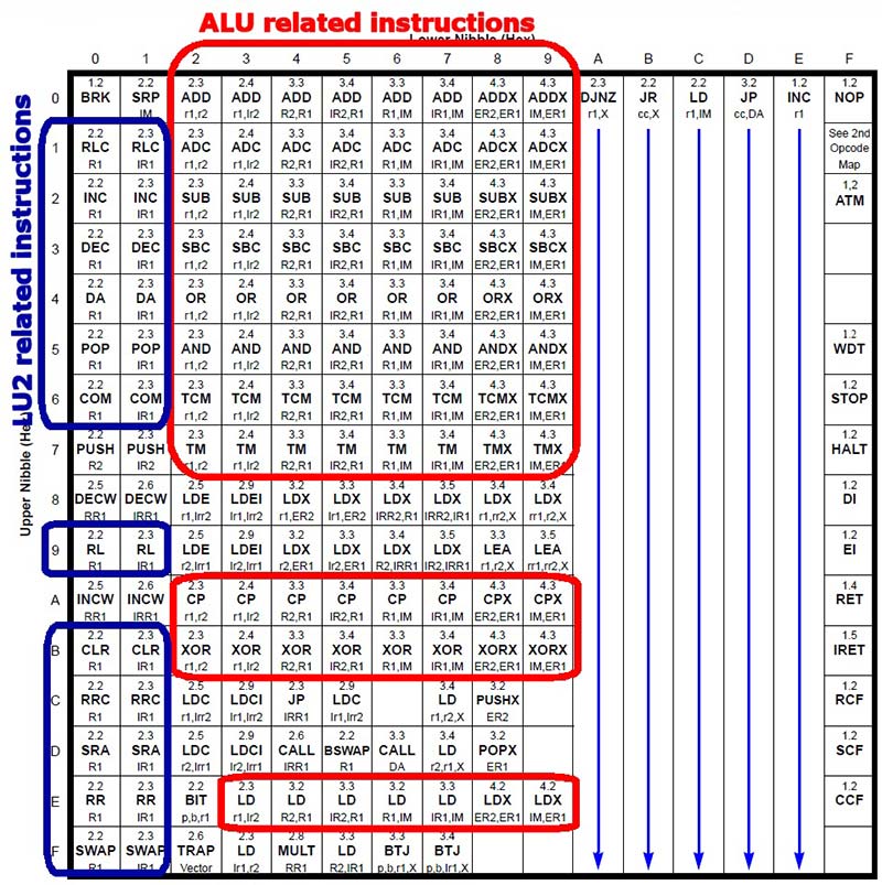
FIGURE 3. Opcodes by groups.
Most instructions can be classified according to some basic rules:
- Columns (the lower nibble of an opcode) usually specify an addressing mode: Column 0x9 instructions, for instance, mostly use the IM,ER1 addressing mode and are four bytes long (the second byte is the immediate operand and the two last bytes are the destination extended address).
- Rows (the higher nibble of an opcode) usually specify an operation: Row 0x0 instructions are mostly addition operations; row 0x2 instructions are mostly subtraction operations, and so on.
If we look at row 0x1, we can see that columns 0x0 and 0x1 are RLC instructions, and columns 0x2 up to 0x9 are ADC instructions. So, we can design an ALU which takes a nibble as input (the higher nibble from the opcode) and decodes it accordingly. While this would work for columns 0x2 to 0x9, we would need another approach for the first two columns.
That is why I ended up writing two units: one ALU which concentrates on most arithmetic and logical instructions; and a second unit (Logical Unit 2, or LU2) which performs other operations shown in columns 0x0 and 0x1 (not all operations seen on those columns are performed by LU2). The operation codes for both ALU and LU2 were chosen to match opcode rows shown in Figure 3.
Another important detail is that all instructions within the same column and group are the same size in bytes, thus can be decoded in the same decoder section.
The decoder design makes use of a large finite state machine (FSM) which advances on each clock tick. Every instruction starts in the CPU_DECOD stat. This is where the decoder actually decodes the opcodes, prepares buses and internal supporting signals, and steps to other execution states. Among all those states, two are widely used by a lot of instructions: CPU_OMA and CPU_OMA2. Can you guess why? If you said because they are related to ALU and LU2, you are absolutely right!
OMA is short for One Memory Access and it is the last state for all ALU related instructions (ADD, ADC, ADDX, ADCX, SUB, SBC, SUBX, SBCX, OR, ORX, AND, ANDX, XOR, XORX, CP, CPC, TCM, TCMX, TM, TMX, and some variants of LD and LDX). On the other hand, CPU_OMA2 is the last state for all LU2 related instructions (RLC, INC, DEC, DA, COM, RL, CLR, RRC, SRA, SRL, RR, and SWAP).
Now, let’s take a look inside the CPU_DECOD state. Refer to Figure 4.
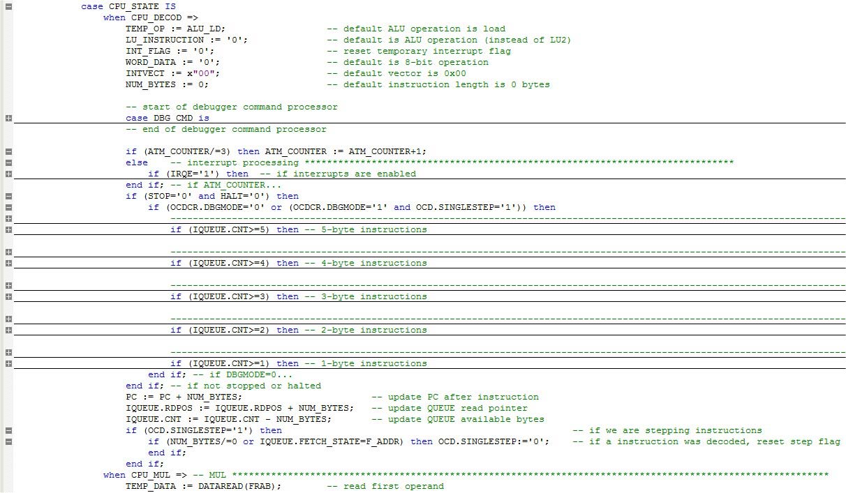
FIGURE 4. CPU_DECOD state.
Within the CPU_DECOD state, we can see that a lot of action takes place. In the beginning, some temporary variables are initialized to a default condition. Note that NUM_BYTES is very important as it controls how many bytes were consumed by the instruction decoder. Its value is used in the last part of this stage to increment the PC (program counter), advance the queue read pointer, and decrement the number of available bytes in the queue.
Following the initialization section, we can see the interrupt processing section. It is responsible for detecting any pending interrupts and prepares the CPU accordingly. I’ll cover this in the next section.
The actual instruction decoding block checks whether a low power mode is not active and also if the debugger mode is off (OCDCR.DBGMODE=0). Or, while in debug mode, a single step debug command was issued (OCDCR.DBGMODE=1 and OCD.SINGLE_STEP=1). It then checks the available bytes in the queue and proceeds with decoding.
Some instructions (mostly the singlebyte ones) are completed within the CPU_DECOD state, while others need multiple states until they are fully completed.
Note that some instruction decoding can make use of several functions and procedures written specially for the FPz8:
- DATAWRITE — This procedure prepares buses for a writing operation. It selects whether the destination is an internal SFR, an external SFR, or a user RAM location.
- DATAREAD — This is a reciprocal function for DATAWRITE. It is used to read a source address and automatically chooses whether it is an internal SFR, an external SFR, or a user RAM location.
- CONDITIONCODE — Used for conditional instructions (such as JR and JP). It takes a four-bit condition code, tests it, and returns the result.
- ADDRESSER4, ADDRESSER8, and ADDRESSER12 — These functions return a 12-bit address from a four-, eight-, or 12-bit source. They use the content of the RP register to generate the final 12-bit address. ADDRESSER8 and ADDRESSER12 also check for any escaped addressing mode.
- ADDER16 — This is a 16-bit adder for address offset calculation. It takes an eight-bit signed operand, sign extends it, adds it to the 16-bit address, and returns the result.
- ALU and LU2 — These were discussed previously, and perform most arithmetic and logic operations.
Interrupt Processing
As I said before, eZ8 has a vectored interrupt controller with programmable priority. At first, I thought this section would not be so difficult because interrupts are no big deal, right? Well, when I started to figure out how to do all the needed tasks (saving context, vectoring, managing priorities, etc.), I realized it would be tougher than I first thought. After a couple hours, I came up with the current design.
FPz8’s interrupt system ended up being simple. It has eight inputs (INT0 to INT7); a global interrupt enable (IRQE bit located in IRQCTL register); two registers for priority setting (IRQ0ENH and IRQ0ENL); and one register for interrupt flags (IRQ0). The design makes use of a nested IF chain which generates a vector address upon detection of an interrupt event regarding an enabled interrupt.
Figure 5 shows a compressed view of the interrupt system. Note there is a first IF statement with a symbol ATM_COUNTER. This is a simple counter used by the ATM instruction (it disables interrupts for three instruction cycles, allowing atomic operations).
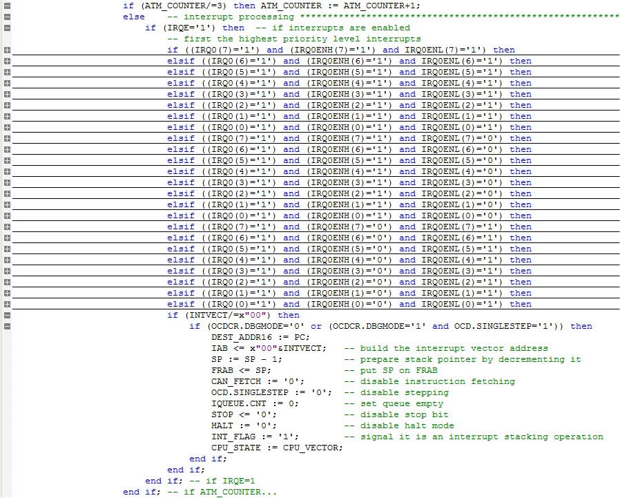
FIGURE 5. FPz8 interrupt system.
One last comment regarding interrupts: The interrupt flag register (IRQ0) samples interrupt inputs every rising edge of the system clock. There are also two buffer variables (IRQ0_LATCH and OLD_IRQ0) which store the current and last state of the flags. This allows interrupt edge detection and also synchronizes the external inputs to the internal clock (FPGAs don’t work well with asynchronous internal signals).
On-Chip Debugger
This is probably the coolest feature of this softcore as it allows a commercial integrated development environment (IDE; such as Zilog’s ZDS-II) to communicate, program, and debug software running on the FPz8. The on-chip debugger (OCD) is comprised of a UART with autobaud capability and a command processor attached to it. The UART performs serial communication with a host PC, and delivers commands and data to the debugger state machine which processes debug commands (the debugger command processing FSM is located inside the CPU_DECOD state).

FIGURE 6. On-chip debugger UART (note the DBG_RX synchronizer).
My OCD design implements almost all commands available on the real hardware, except for those related to data memory (debug commands 0x0C and 0x0D); the read runtime counter (0x3); and the read program memory CRC (0x0E).
One thing I would like to highlight is care is needed when dealing with asynchronous signals inside FPGAs. My first design didn’t account for that while processing the DBG_RX input signal. The result was absolutely weird. My design had worked flawlessly in simulation. I downloaded it to an FPGA and started playing around with the debug serial interface by using a serial terminal (my FPGA board has a built-in serial-USB converter).
To my surprise, while most of the time I could successfully send commands and receive the expected results, sometimes the design would simply freeze and stop responding. A soft reset would make things go back to their proper operation, but that was intriguing me. What was happening?
After a lot of tests and some Googling, I figured out that it was possibly related to the asynchronous edges of the serial input signal. I then included a cascaded latch to synchronize the signal to my internal clock and all the problems were gone! That is a tough way to learn that you must always synchronize external signals prior to feeding them into complex logic!
I must say that debugging and refining the debugger code was the hardest part of this project; mostly because it interacts with all the other subsystems including buses, the decoder, and instruction queue.
Synthesizing and Testing
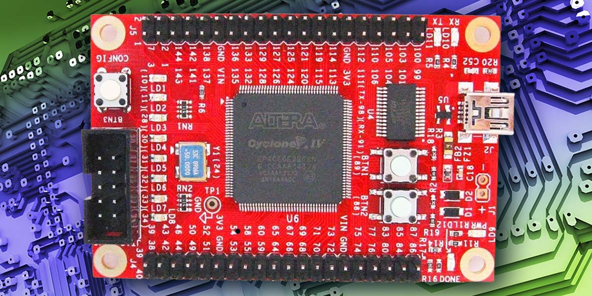
Once fully compiled (I used Quartus II v9.1 sp2), the FPz8 core used up 4,900 logic elements, 523 registers, 147,456 bits of on-chip memory, and one embedded nine-bit multiplier. Overall, the FPz8 uses 80% of the EP4CE6’s available resources. While this is a lot, there are still some 1,200 logic elements available for peripherals (my simple 16-bit timer adds up to around 120 logic elements and 61 registers). It even fits on the smallest Cyclone IV FPGA — the EP4CE6 — which is the one mounted on the low cost mini board I used here (Figure 7).
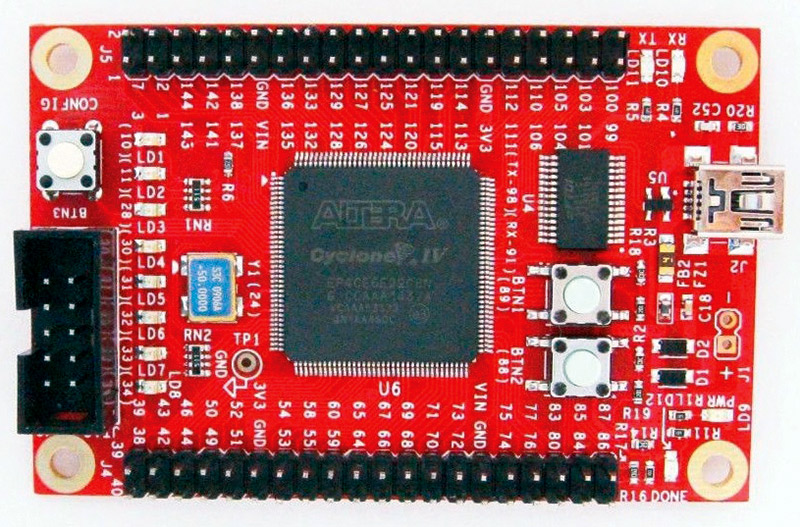
FIGURE 7. Altera Cyclone IV EP4CE6 mini board.
The mini board features (along with the EP4CE6 device): an EPCS4 serial configuration memory (mounted on the bottom side); an FTDI serial-to-USB converter chip as well as a 50 MHz crystal oscillator module; some buttons; LEDs; and pin headers to access FPGA pins. There is no integrated USB-Blaster (for FPGA programming), but the package I bought also included an external programming dongle.
As for the real world tests, needless to say, the FPz8 didn’t work the first time! After thinking a bit and reading compiler output messages, I figured out that it was probably a timing issue. This is a very common dilemma when designing with programmable logic, but as this was my second FPGA design ever, I didn’t pay enough attention to it.
Checking the timing analysis messages, I could see a warning that the maximum clock should be around 24 MHz. At first, I tried using a divider-by-2 to generate a 25 MHz CPU clock, but it wasn’t reliable. I then used a divider-by-3. Everything started to work perfectly!
That’s why FPz8 currently runs at 16.666 MHz. It is possible to achieve higher speeds by using one of the internal PLLs to multiply/divide the main clock in order to get a resulting clock lower than 24 MHz, but higher than 16.666 MHz.
Programming and Debugging
Using the FPz8 is very simple and straightforward. Once the design is downloaded to the FPGA, the CPU will start running any program loaded in memory. You can supply a hex file and use the MegaWizard Plug-in Manager to change the program memory initialization file. That way, your application code will start running following a reset signal.
You can use the Zilog ZDS-II IDE to write Assembly or C code, and generate the necessary hex files (I usually select the Z8F1622 as my target device as it also has 2 KB of RAM and 16 KB of program memory). Thanks to the on-chip debugger, it is also possible to use the ZDS-II IDE to download code to the FPz8 using a serial debug connection (USB, in our case).
Before connecting, make sure that debugger settings are the same as in Figure 8. Uncheck the “Use page erase before flashing” option, and select “SerialSmartCable” as the current debug tool. Don’t forget to also check if the FTDI’s virtual COM port is correctly selected as the debug port (use the Setup button). You can set the desired communication speed as well; 115,200 bps works very well for me.
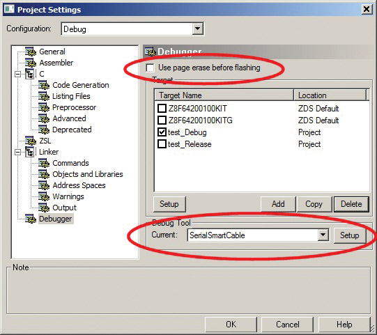
FIGURE 8. Debugger settings.
Note that when connecting to the FPz8, the ZDS-II IDE will show a warning message informing you that the target device is not the same as the project. That happens because I didn’t implement some ID memory areas. Just ignore the warning and proceed with the debugging session.
Once the code is successfully downloaded, you can start the application (GO button), step instructions, inspect or edit registers, set breakpoints, etc. As with any other good debugger, you can, for example, select the PAOUT register (under PORTS group) and even change the state of the LEDs connected to PAOUT.
Some simple C code examples can be found in the downloads.
Just keep in mind that the FPz8 has a volatile program memory. Thus, any program downloaded to it is lost when the FPGA is powered down.
Closing
This project took me a couple weeks to complete, but it was delightful to research and design a microcontroller core.
I hope this project can be useful for anyone wanting to learn about computing basics, microcontrollers, embedded programming, and/or VHDL. I believe that — if paired with a low cost FPGA board — the FPz8 can provide a fantastic learning (and teaching) tool. Have fun! NV
References
CEFET-PR:
www.utfpr.edu.br
ScTec:
www.sctec.com.br
HCS08 Unleashed:
https://www.amazon.com/HCS08-Unleashed-Designers-Guide-Microcontrollers/dp/1419685929
Zilog eZ8 CPU Manual (UM0128):
www.zilog.com/docs/UM0128.pdf
Zilog Z8F64xx Product Specification (PS0199):
www.zilog.com/docs/z8encore/PS0199.pdf
Zilog ZDS II IDE User Manual (UM0130):
www.zilog.com/docs/devtools/UM0130.pdf
Zilog ZDS-II Software Download:
https://www.zilog.com/index.php?option=com_zcm&task=view&soft_id=7&Itemid=74
Zilog Microcontroller Product Line:
http://zilog.com/index.php?option=com_product&task=product&businessLine=1&id=2&parent_id=2&Itemid=56
Project Files available at:
https://github.com/fabiopjve/VHDL/tree/master/FPz8
FPz8 at Opencores.org:
http://opencores.org/project,fpz8
Downloads
What’s in the zip?
Source Code Files