If you work with digital and logic circuits (and we all do), you will find this instrument handy for design, troubleshooting, and calibration of electronic circuits. Although I own a somewhat expensive commercial function generator, I find that this pulse generator is the one I reach for most of the time. The generator is fairly easy to build and uses a straightforward design. It requires six integrated circuits and two transistors. In addition, you will need a power supply of 15 volts at 200 mA.
You may build this unit as shown or add/delete stages if you prefer something more customized for your needs. In two years of use, I have not felt any need to change the design, as it has worked well under all situations.
I housed this unit in a 7 x 4 x 5-inch box. If you build it exactly as shown, do not use a box any smaller than this, as you will be crowding the front panel controls. Before we get into the construction, I feel that a description of the theory of operation is in order.
How It Works
Referring to the schematic (Figure 1), the heart of the unit is the U4 rate generator and the U3B width generator. The U4 multivibrator rate is set in six steps by capacitor selection of S6a, S6b.
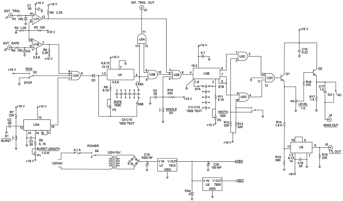
FIGURE 1. The heart of the unit is the U4 rate generator and the U3B width generator.
This, in turn, is varied by potentiometer P2 to give complete coverage between bands. The RATE change is two microseconds to one second continuous with R9 and P2 values giving an approximate 10 percent overlap between ranges. The squarewave output is sent through U5a,b (AND gate), which provides buffering to U4. One gate sends the signal to J3 (internal trigger out). The other gate sends the signal to U2b-P5, which isolates the various inputs from each other by an OR gate function.
The positive edge from the output of U2b triggers the width generator, U3b. Incidentally, all of these circuits are positive-edge triggered. U3b is a monostable multivibrator, and its output width is determined by capacitor selection via S7a, S7b. As in U4, it is varied by potentiometer P3 (also providing a 10 percent overlap) to provide continuous converge from one microsecond to 100 milliseconds in width. The output of U3b is sent through U2c to the base of Q1. In conjunction with S4, U5c and d provide the option of positive- or negative-going pulses (Q or Q not).
The pulse level at this point is 15 volts peak, and the job of emitter follower Q1 is to drive the pulse-level control P4 and the translator circuit R14, R15 to operate TTL level U6 for the rapid rise and fall times required by this family of circuits.
From the output of the pulse-level control, the pulse is sent to Q2 via R16. Q2 is a current amplifier to drive very low impedance loads. Its output impedance is on the order of 10 ohms and will easily drive 50-ohm loads at five-volt logic levels.
The main output at J4 is AC or DC coupled, as selected by S5. The output at this point is zero to 14 volts, peak. R17 is a pull-down resistor to help speed up fall times. R16 was arbitrarily chosen to reduce overshoot and ringing.
Switch S2 (run-stop) provides several options. In the run position, the U4 rate generator runs continuously and provides the trigger for U3b. In the stop position, U3b triggering can be any of the following:
- Externally triggered through J1
- Single shot triggered via S3 (single) — one pulse per depression
- Externally gated through J2
- Internally burst triggered via S1 (burst) — one burst per depression
U1 and U2 are identical high-speed comparators and will accept any wave shape from dc to 1 MHz. Their input voltage range is from 1.3 to 15 volts, peak. The input impedances are one megohm. U3a is the burst length generator and will send out one group of pulses every time S1 is depressed. The actual amount of pulses is determined by the front panel control settings and the burst-length time chosen by potentiometer P1. In my unit, I chose a range of 0.1 to 20 milliseconds for this circuit. You can vary yours by changing the RC time constant of P1, C3.
C1 and C2 provide a cheap means of debounce for the contacts of S1 and S3, respectively. The main output (J4) has a pulse rise time of 10 nanoseconds and is compatible to complementary metal-oxide semiconductor (CMOS) or bipolar circuitry. The TTL output (J5) is compatible for this type of circuitry, as mentioned previously. The features built into this generator have sufficed for all my needs. Now, on to construction.
Construction
As I mentioned earlier, the box I used would be as small as you want to go. I even had to mount most of the power supply components on a back inside corner of it and mount the power-on switch on the back of it.
FIGURE 2. The power switch is located on the back of the case.
I am not going to dwell on power supply construction, as you can use any configuration you like, even to the extent of incorporating a wall transformer, if necessary. Just make sure that it will fulfill the circuit requirements of 18 to 22 volts and a minimum of 200 mA.
I built the actual circuit on a perf board with traces that would accept dual inline package (DIP) sockets. I always use sockets in my projects for future modifications or troubleshooting. This board was 3.25 x 5.5 inches and was laid out as shown in Figure 3. Almost all of the components were installed on the board with the exception of C5 through C15, which I will address shortly.
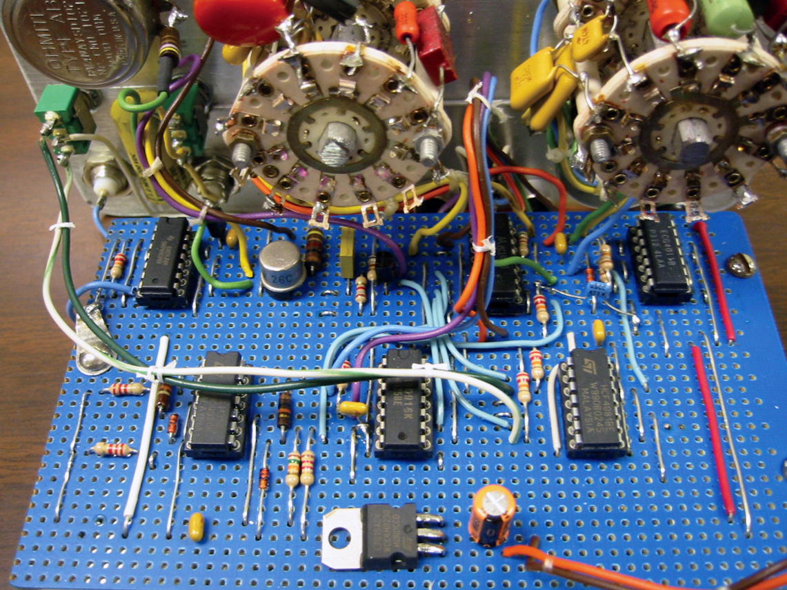
FIGURE 3. The board is 3.25 x 5.5 inches.
Q2 was chosen for its high-speed operation and power handling ability. Most high-speed switching transistors will work fine, and even the lowly 2N3904 performed satisfactorily in this circuit. C16 should be mounted close to this collector. No circuit layout problems were encountered in this construction, even with the front panel wires grouped and laced. J1, J2, and J3 are all accessible through a cutout in the back wall of the housing.
As for the timing capacitors, C5 through C15, I elected to mount these between the decks of rotary switches S6 and S7. When the associated variable controls (P2 and P3) are in their calibrated position (fully counterclockwise), the rates and widths will be as marked on the front panel switch positions. These are as follows:
RATE:
2 µsec, 10 µsec, 100 µsec, 1 msec, 10 msec, 100 msec
WIDTH:
1 µsec, 10 µsec, 100 µsec, 1 msec, 10 msec
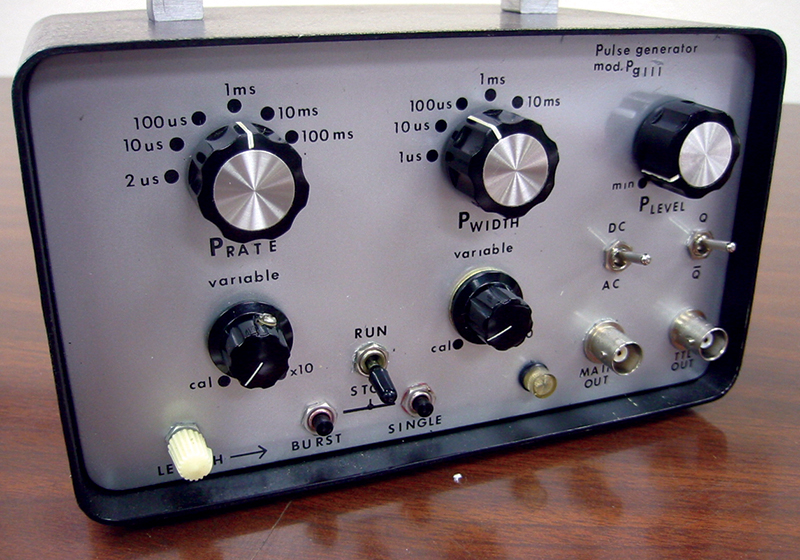
FIGURE 4. The rates and widths are marked on the front panel.
The variable controls will take you from one range up to the next, with a 10 percent overlap to ensure complete coverage. In the calibrate position, accuracy will depend on how close the capacitor values are to the required values.
On some ranges, I nailed it on the first capacitor picked. On others, I had to sneak up on it with two capacitors (one large, one small). I aimed for one-percent accuracy on all ranges, and it was not difficult to obtain this. There is no point in trying for greater accuracy than this, as capacitor stability will not guarantee the timing will remain that stable. If you want greater stability and accuracy, you will have to use expensive polystyrene or similar capacitors.
These extreme accuracies are really not necessary, as you will usually be using this unit in conjunction with other test equipment (scopes, etc.) for cross-checking. The parts list shows the target values of capacitors C5 through C15. These values may vary in your particular circuit, but offer a close starting point.
Also, the potentiometers (P2 and P3) can be shunted with high-value resistors to slightly alter their values and bring the low-end timing (P2 and P3, fully clockwise) more in line with the expected rates and widths at these points. The important function in these two circuits is not so much that you have front panel accuracy, but rather that you have complete coverage across the switched bands.
The actual output drive current that the generator will produce depends on transistor Q2 and the duty cycle (percentage of time that Q2 remains at a high-level voltage). For the transistor shown, it will deliver 500 mA at a 10 percent duty cycle with no degradation in pulse specs. For an example, a 2N3904 would deliver 100 mA under the same conditions.
For U6 (cmos to TTL translator), I used a hex inverter only because it was handy. Any TTL gate configuration is suitable; just make sure the output remains non-inverted with respect to the input.
Upon completion, if you encounter problems, start by checking the power supply sources (+15 and +5 volts). Then look at rate generator U4 to make sure it is running. U4 will run when U2a-P9 is positive and stop when it’s negative. Beyond the generator and due to circuit simplicity, you can go stage by stage using standard troubleshooting techniques.
When you finish this project, you will have a source of pulse generation capable of a wide range of outputs:
Rate — continuously variable from two microseconds to one second
Width — continuously variable from one microsecond to one millisecond
Trigger — continuous, single burst, internal or external
Output — adequate drive for virtually any circuitry (zero to 14 volts, peak)
Personally, this was an interesting and fun project to build and has proved to be an essential piece of gear to my test bench. Take your time building this, do a professional job, and you will be as satisfied as I am. NV
PARTS LIST
Resistors
[5% 1/4 watt] |
Capacitors
[25 volt or more] |
Semiconductors |
| R1 |
10K |
C1 |
0.05 µF |
D1,D2,D3 |
IN914 |
| R2 |
1.2K |
C2 |
0.05 µF |
RB1 [bridge] |
100V@1A |
| R3 |
15K |
C3 |
0.05 µF |
Q1 |
2N3904 |
| R4 |
10K |
C4 |
0.05 µF |
Q2 |
2SC730 |
| R5 |
2.2K |
C5 |
5.5 µF [non electrolytic] |
U1 |
LM319 [dual comparator] |
| R6 |
2.2K |
C6 |
0.56 µF |
U2 |
CD4075 [triple 3 input OR gate] |
| R7 |
22K |
C7 |
0.056 µF |
U3 |
CD4528 [dual monostable] |
| R8 |
5.1K |
C8 |
0.0056 µF |
U4 |
CD4011 [quad NAND gate] |
| R9 |
9.1K |
C9 |
560 pF |
U5 |
CD4081 [quad AND gate] |
| R10 |
22K |
C10 |
51 pF |
U6 |
SN7404 [hex inverter] |
| R11 |
5.1K |
C11 |
5.7 µF [non-electrolytic] |
U7 |
7815C [+15V reg.] |
| R12 |
22K |
C12 |
0.56 µF |
U8 |
78L05C [+5V reg.] |
| R13 |
22K |
C13 |
0.056 µF |
Miscellaneous |
| R14 |
1.8K |
C14 |
0.0039 µF |
P1 |
1.0 Omegohm [BURST LENGTH] |
| R15 |
680Ω |
C15 |
130 pF |
P2 |
100K [RATE VARIABLE] |
| R16 |
470Ω |
C16 |
0.22 µF |
P3 |
50K [WIDTH VRIABLE] |
| R17 |
1K |
C17 |
1.0 µf-50V |
P4 |
1K [LEVEL] |
| R18 |
22K |
C18 |
0.05 µF |
S1, S3 |
Momentary NC |
| C19 |
1000 µF-35V |
S2, S4, S5, S8 |
Toggle SPDT |
| C20 |
100 µF |
S6, S7 |
Wafer [2 deck] 6 Position |
| J1-J5 |
BNC Female |
| Pilot |
LED with int. Resistor |
| T1 |
120V primary; 15-20V
secondary @ .25A |