This article addresses the subject of semiconductor-based temperature measurement. The theory is developed in a general way and then applied to the construction of a device useful to those of us who spend many hours at our workbench or desk. It’s hoped that the presentation is such as to suggest to the reader many possible variations and other applications.
Several articles have appeared in Nuts & Volts over time regarding workbench construction and outfitting, but none have addressed that almost-universal need: a means of keeping the contents of one’s coffee cup warm.
This coffee cup warmer project evolved out of a study of the means of temperature measurement using a semiconductor junction (see Resources).
Applications in which large changes of temperature occur or where it’s unnecessary to know the actual temperature value can be detected by monitoring the voltage drop across an ordinary signal diode, whose junction voltage changes at about -2 millivolts per degree C. For a fire alarm application, for example, a couple of hundred degrees temperature change can be readily detected using a simple amplifier without concern about component manufacturing variations or origins.
Temperature monitoring where a value is to be displayed, however, or from which the measurement can provide feedback to hold a temperature constant, requires a more sophisticated technique in order that such variations in the components used to effect measurement need not be considered. Such is the case in this design.
The idea of having a heated plate with temperature-controller circuitry mounted underneath dictated the overall structure. The device should be easy to control, requiring merely an on/off switch and a one-time temperature setability. It should be electrically safe, implying a power source isolated from the utility mains. It must not constitute a fire hazard should the controller fail in the heater-powered state. And it should be mechanically stable.
The resulting design is shown in Figure 1, consisting of a 5/16” thick triangular aluminum plate of 6”x6”x6” dimension about 2-1/2” tall, standing on three legs, and having the controller PCB (printed circuit board) mounted underneath, all coupled together with threaded standoffs.
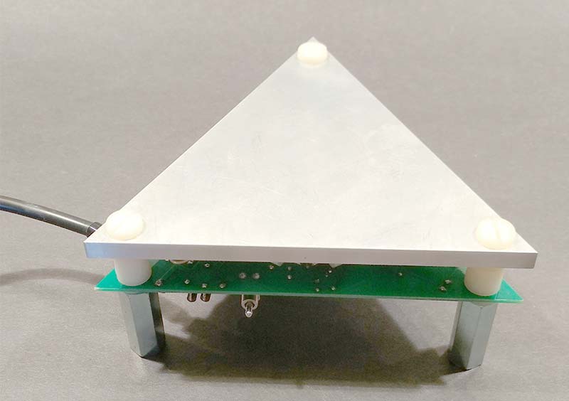
FIGURE 1. An overview of the completed heater assembly.
The coffee heater element consists of nine 5 ohm/10 watt power resistors connected in series and is bolted to the underside of the top surface of the coffee heater assembly; see Figure 2.
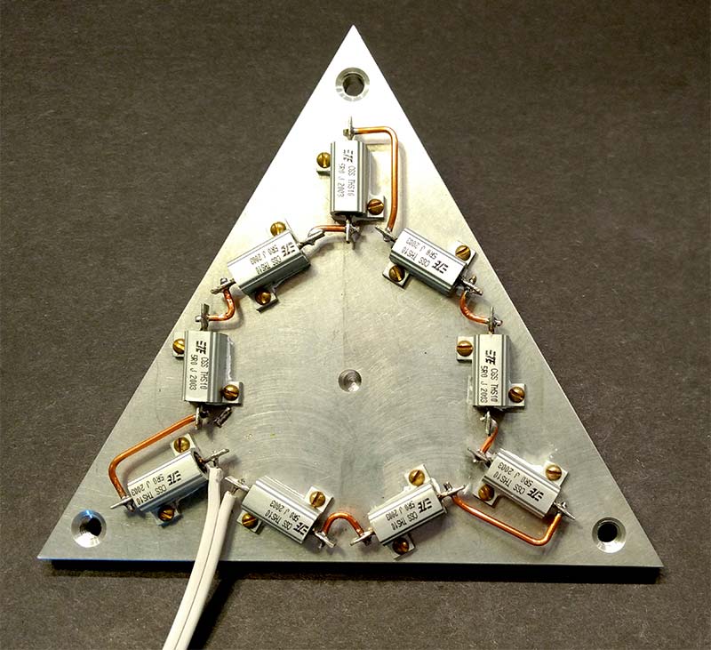
FIGURE 2. Underside of heater plate showing mounted heater resistors.
The heater was tested under continuous power to simulate a controller failure and was found to self-limit at about 165°C. Refer to Figure 3.
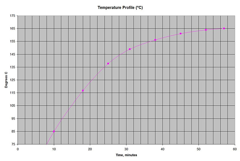
FIGURE 3. Continuous power-on test showing heater temperature vs. time.
Circuit Theory
The measurement of temperature using a bipolar device relies on the characteristics of the P-N junction. Although a simple diode can be used, better performance is realized when a transistor is used in an “active diode” configuration with its base and collector connected together.
Figure 4 shows such an active diode conducting current provided by a current source Ic and exhibiting a base-emitter voltage differential Vbe.
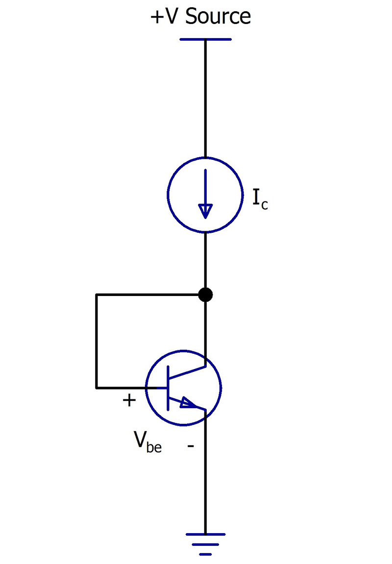
FIGURE 4. “Active diode” circuit.
In this configuration, the transistor is still active with current gain hfe, so that the base resistance of the device is reduced by the multiplier:

resulting in a device having a diode characteristic close to ideal over a significant range of current.
It can be shown that the relationship between device voltage, current, and temperature is given by:
Equation 1-a.
where
Ic = Collector current
Is = Reverse bias saturation current
Vbe = Base-emitter voltage
q = Absolute value of the electron charge = 1.602 × 10⁻¹⁹ coulombs (= joules/volt)
k = Boltzmann’s constant = 1.381 x 10⁻²³ joules/°K
T = Junction temperature, °K (i.e, absolute temperature, degrees Kelvin)
n = Ideality factor
We can see that Ic is an exponential function of absolute temperature, Vbe and a bunch of constants. The ideality factor n — while process-related — is generally taken to be = 1, especially for a diode-connected small-signal transistor such as a 2N2222 or 2N3904. The quantity:

has the units of voltage; it varies directly with temperature at a rate of 86.2 µV/°K.
The “-1” term in Equation 1-a is required in order that Ic = 0 when Vbe = 0, but for practical applications, it may be ignored, and this simplifies the process when solving for Vbe from Equation 1-a:

Equation 1-b.
Is, however, is process related and roughly doubles in value for every 5°K temperature rise, which means that we’d like to get rid of this factor in Equation 1-b. One technique commonly used is to force a pair of well-controlled currents Ic1 and Ic2 alternately through the active diode and measure the difference in values of base-emitter voltage Vbe1 and Vbe2:
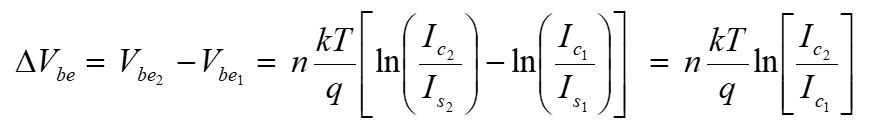
Equation 2.
If we set up our circuitry so that  = 10, and 1n[10] = 2.3, hence:
∆Vbe = 1 × 86.2 ×10-6 × 2.3 = 198 µv/°K per decade of change in collector current.
For such a setup: ∆Vbe at 0°C (273°K) = about 54 millivolts; at 100°C (373°K), ∆Vbe = about 74 millivolts.
Circuit Description
The schematic diagram of the cup heater controller board is shown later in Figure 11. The temperature measuring element is Q2, an NPN transistor configured as an “active diode.” Its base-emitter voltage V is observed at its collector-base connection, relative to ground (Net 3).
A current is impressed upon Q2 by PNP transistor Q1, whose base is held at 9.99 volts above ground by voltage divider resistors R5 and R6. The value of Q1’s emitter current is equal to the collector current at Q2. Q1’s emitter current is provided from the 15V bus through several paths, depending on the state of switch U2.
This IC contains four semiconductor single-pole/double-throw (SPDT) switches plus an oscillator circuit which causes all four switches to alternate state in synchronism; approximately 200 times per second in this design. The oscillator frequency is set by the value of C3.
Figure 5 illustrates the relationship between collector current and base-emitter “on” voltage for Q1. Note that the (red line) slope of the curves:

is such that for small collector currents, Vbe increases about 0.06 volts for every decade of increase in collector current. Figure 5 suggests that Vbe2 ≈ 0.58 volts for Ic2 = 100 µA. It follows that for Ic1 = 10 µA and at the same temperature, Vbe1 will be about 60 millivolts less, or ≈ 0.52 volts.
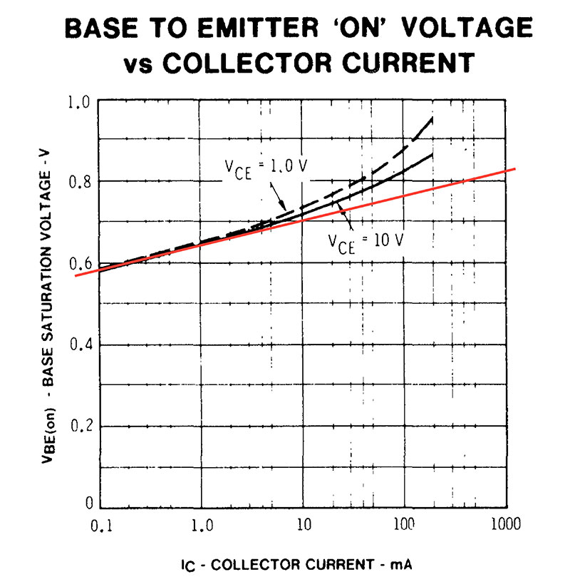
FIGURE 5. Base saturation voltage as a function of collector current.
When the switch elements in U2 are in the state shown in the schematic, Q1 is supplied emitter current through resistors R1 and R2. So, Q1’s Vbe1 ≈ 0.52 volts (refer back to Figure 5), placing 4.49 volts across the sum of resistances R1 and R2 — 516K ohms — causing about 8.7 µA = I to flow into the emitter of Q1 and hence into Q2 (Figure 6).
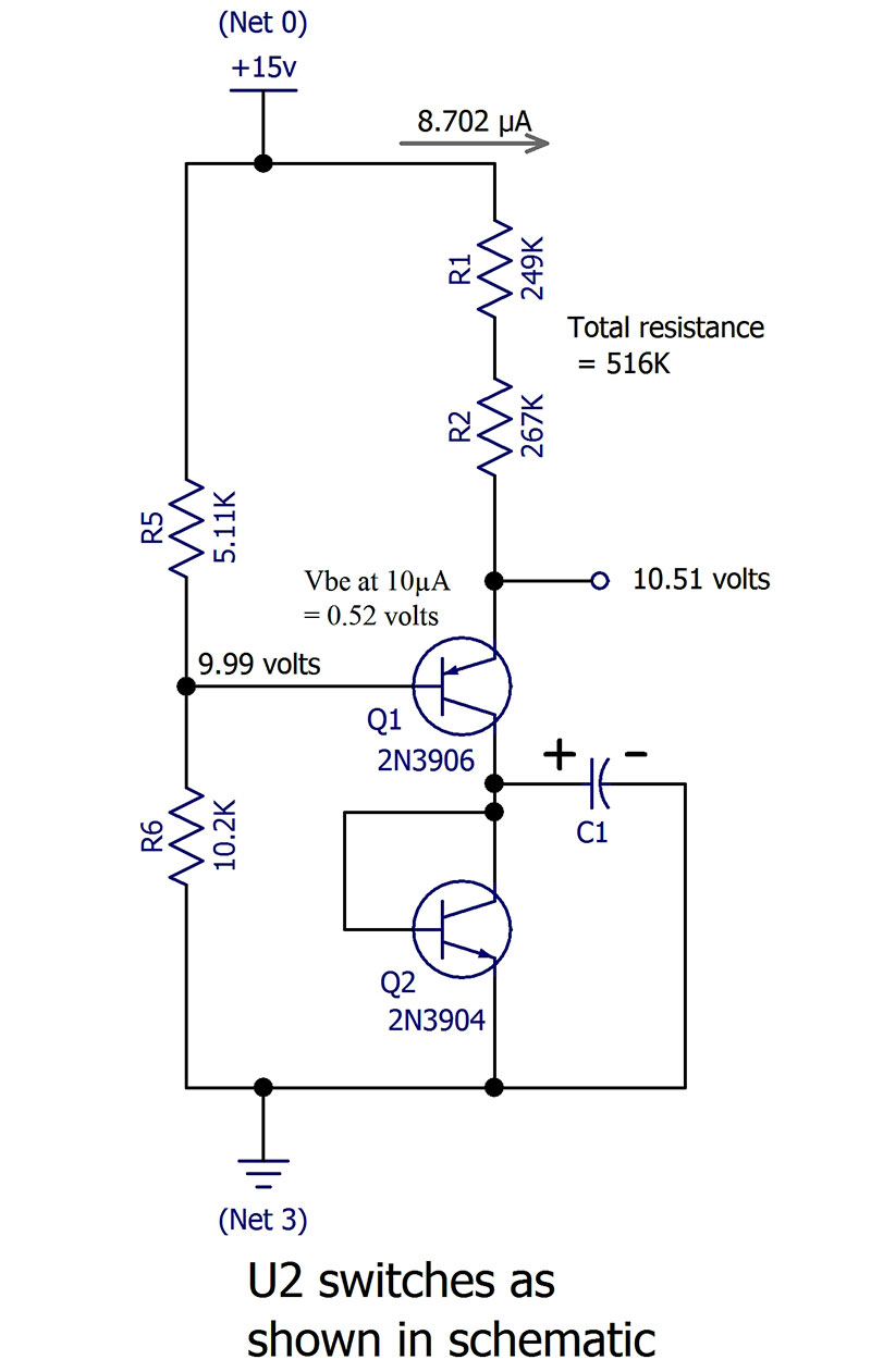
FIGURE 6. Vbe1 generated by current Ic1 impressed on C1.
Because switch element U2-2 is connected to U2-6 at this time, the “-” end of capacitor C1 is connected to ground, so Q2’s base-emitter voltage will be impressed upon C1 with the polarity shown.
When U2 changes to the opposite state (Figure 7), switch element U2-12 connects to U2-14, and therefore the current through Q1 and Q2 becomes determined by voltage across the parallel combination of R1-plus-R2 and R3-plus-R4 plus the internal resistance of the switch pole, effectively 46.5K ohms.
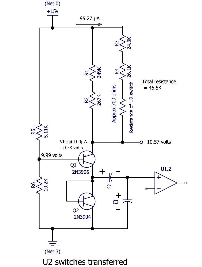
FIGURE 7. ∆Vbe = Vbe2, as generated by current Ic2, minus the voltage Vbe1 on C1, impressed on C2, and passed to amplifier U1.2.
For Vbe2 ≈ 0.58 volts, the voltage across these resistors will be about 4.43 volts, pulling about 95 µA = I through Q1 and Q2.
At the same time as switch element U2-12 connects to U2-14, switch element U2-2 connects to U2-5, causing the end of C1 to be connected to C2.
Because of the polarity of the charge on C1, as indicated in Figure 7, the base-emitter voltage at Q1 during the previous half-cycle Vbe1 (taken at the same temperature but with the smaller collector current) will be subtracted from its present value, Vbe2, so that the voltage impressed upon C2 and provided to amplifier U1.2 will be Vbe2 – Vbe1 = ∆Vbe which is exactly the objective of the exercise.
The ratio of the computed values for Ic1 and Ic2 is approximately 11:1. For n = 1, for the component values given, and using Equation 2 above, at 0°C = 273°K:

In the present application, temperatures in excess of 100°C are required: e.g., ∆Vbe = 87.3 mV at 150°C. The measurement span over the 0° to 150°C temperature interval is 31.0 mV, or 207 µV per °C. The purpose of amplifier U1.2 and its associated circuitry is to scale these ∆Vbe values in order that an output range between 0 and 10 volts will represent temperatures between 0° and 150°C.
For U1.2 to output 0 volts at 0°C, it is necessary to provide a matching offset voltage to U1.2; this function is provided by U3 (a precision 2.500 volt reference), along with voltage divider R8 through R11.
The needed reference voltage (Vref) of 56.3 mV is developed across R10 and R11. U1.2 is configured as a non-inverting amplifier with an inverting positive reference (Figure 8).
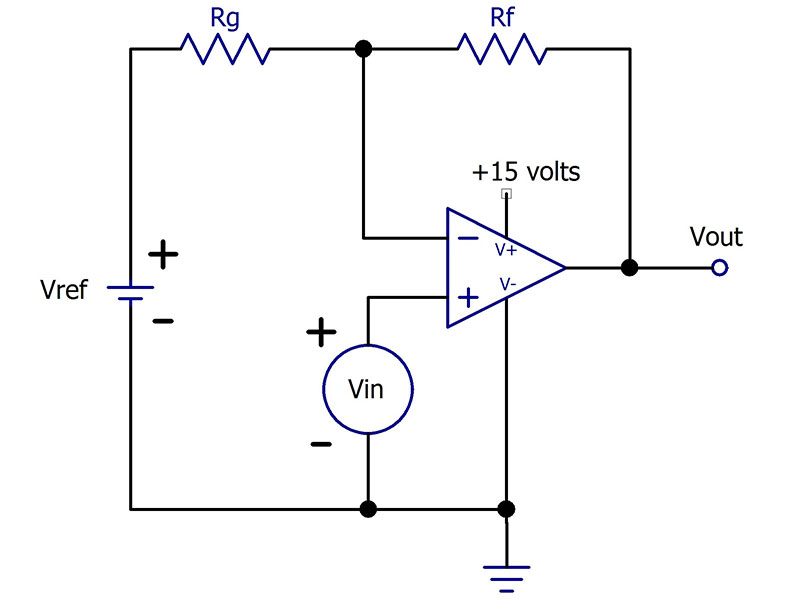
FIGURE 8. Non-inverting amplifier with an inverting positive reference.
For this configuration:
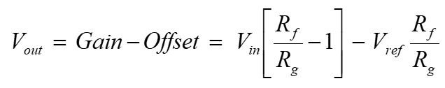
Equation 3.
Equation 3 is a combination of the expressions for the gains of:
a non-inverting amplifier 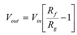
and an inverting amplifier 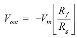
in which the minus sign signifies signal inversion.
We can rewrite Equation 3 to solve for the ratio:
Equation 4.
which expresses the amplifier gain required.
The objective is that for T = 150°C = 423°K, Vout shall be = 10 volts for Vin = 87.3 mV; and also that Vref = 56.3 mV, so:
In the present application, Rf is the feedback resistance R12 and Rg is the reference resistance R14. The value of R14 must be sufficiently large that feedback currents through R12 do not affect Vref, so after juggling values, Rg = R14 was set = 2.00K ohms, whereupon Rf = R12+R13 = 641K ohms using Equation 4.
The heater resistors (refer back to Figure 2) are powered from the 48 volt DC bus (Net 23). Power to the resistors is switched by RLY1 which, in turn, is controlled by Q3. Diode D1 is a “catch” diode, preventing inductive voltage kickback from harming Q3 at relay coil turn-off.
Q3 is controlled by U1.1, an amplifier configured as a Schmidt-trigger comparator. U1.1 compares the output voltage from U1.2 — representing the temperature measurement — with a level set by voltage divider R16, R19, and R17. As constructed, potentiometer R19 can select a voltage level between 8.4 and 11.7 volts, representing a temperature setting of about 126°C to 175°C. Resistor R21 introduces about one-quarter of a volt of hysteresis into the system to avoid chattering.
If R19 is set at mid-point — about 10 volts — and if Q3 and RLY1 are on (supplying energy to the heater resistors), the input voltage provided from U1.2 must exceed about 10.1 volts for U1.1’s output to change state and go low to about zero volts, thereupon Q3 and RLY1 turn off. Conversely, as the heater cools, the output voltage from U1.2 will eventually drop below about 9.9 volts, whereupon U1.1 changes state again, its output goes high (to about 15 volts), Q3 and RLY1 turn on, and heating resumes. D6 is a bicolor indicator LED. When the heater is on, Q4 conducts, passing current left to right through the yellow diode and R24. When the heater is off, Q5 conducts, pulling current through R15 and the green diode.
Power for the cup heater assembly is provided by an external 48 volt regulated DC power supply; the one specified in the Parts List works nicely, but any other having similar characteristics would be suitable. Capacitors C5, C8, and C9 provide local energy storage and D3 protects against inadvertent reverse polarity application.
There are four power supply busses in the cup heater circuitry, denoted by their net names:
- Net 23: +48 volts
- Net 0: +15 volts
- Net 3: Measurement circuit common return
- Net 17: Heater circuit common return
The 15 volt power for the measurement circuitry is provide d by three-terminal regulator U5 which takes its input from the 48 volt bus, reduced by the two 12 volt Zener diodes D4 and D5. Diode D2 protects the regulator from sudden loss of input voltage.
When laying out the PCB for this, it was desirable to keep the measurement and heater-power common returns separate, which was easiest to accomplish by joining them at one manually-selectable point with a “zero ohm” jumper. Connection to the support frame is effected from this place as well.
Referring again to Figure 2, the reader will note a blind hole located in the center of the triangular plate. Temperature-sensing transistor Q2 (2N3904) is mounted to the solder (reverse) side of the PCB; it is so positioned that its body fully enters the hole and any remaining spaces therein are filled with thermal compound.
The reader will note that all the resistors in the temperature measurement circuitry are of 0.1% tolerance, effecting predictable outcomes and temperature stability. Sometimes two resistors are used in series or parallel as a work-around technique because Mouser doesn’t stock all the possible values of 0.1% tolerance 1/4 watt resistors.
Having segregated the common-return circuits as noted previously, the PCB design proceeded in a straightforward manner; the only difficulties being sure to reverse the connections to Q2 because it’s mounted on the opposite side of the board and fitting all the components into the available space and shape while leaving space for the mounting hardware. The completed PCB assembly is shown in Figure 9.
FIGURE 9. Assembled PCB.
The PCB layout is shown in Figure 10.
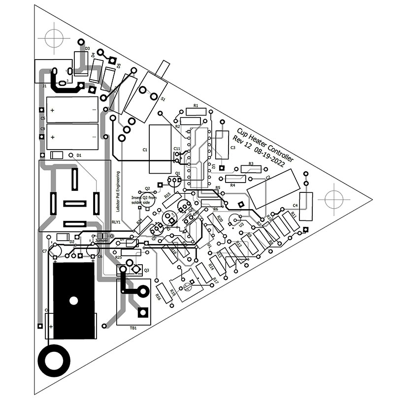
FIGURE 10. PCB layout of the cup heater controller board. Note the inverted configuration for Q2 at the center of the board.
The schematic diagram of the cup heater controller board is shown in Figure 11.
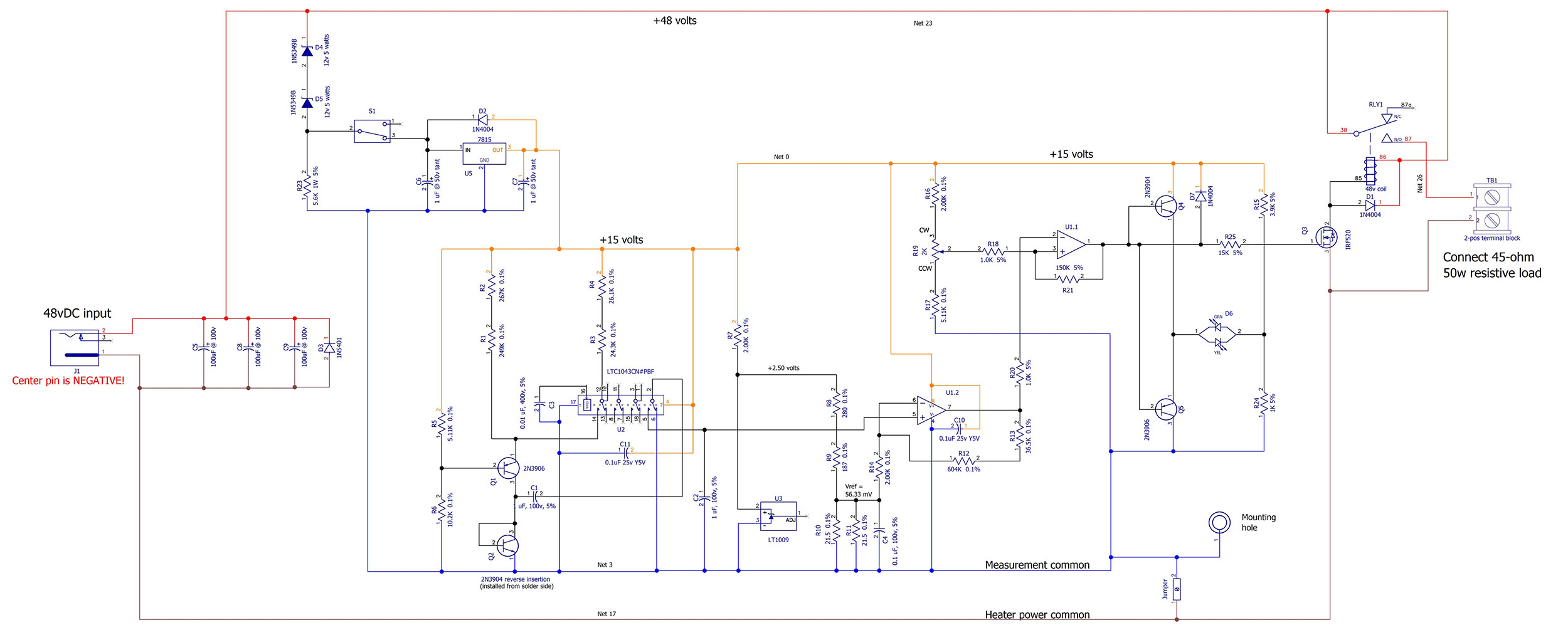
FIGURE 11. Schematic diagram of the cup heater controller board. A full size schematic is available with the article downloads.
The most time-consuming part of the job involved the heater plate mechanical design, getting all the necessary holes positioned as needed, and coordinating these with the PCB layout. The resistors are secured with #2-56 screws. The male-female 1/2” hex mounting hardware required 1/4”-20 threaded through-holes. Except for the latter, all the holes in the plate are blind in order that no holes interrupt the continuous surface of the heater plate.
Heater plate mechanical details, PCB artwork, a full-size schematic, and a bill of materials are available at the article link. Data and commentary regarding LT-Spice simulations at 0°, 25°, and 150°C will also be found at the same place.
Time for a cup of hot Joe … NV
Parts List
| Ref/Description |
Value |
Name |
Qty |
Manufacturer |
Vendor |
| RLY1 |
48V coil |
Relay SPDT |
1 |
Bosch |
Amazon |
| C6,C7 |
1 µF @ 50V tant |
1 µF @ 50V tant |
2 |
Kyocera |
Digi-Key |
| Coaxial power plug for external DC power supply |
|
2.5 x 5.5 mm solder |
1 |
CUI INC |
Digi-Key |
| D1,D2,D7 |
1N4004 |
1N4004 |
3 |
Micro Commercial |
Digi-Key |
| D6 |
Grn/Yel bicolor |
LED T-1-3/4 Grn/Yel bicolor |
1 |
Kingsbright |
Digi-Key |
| Heater resistors |
5 ohms, 10 watts |
Aluminum housed resistor MIL-RE60 |
9 |
Tyco Electronics |
Digi-Key |
| J1 |
Receptacle, R/A, through-hole |
2.5 x 5.5 mm PCB mount |
1 |
CUI INC |
Digi-Key |
| Jumper |
Zero ohm axial 1 |
|
1 |
Yageo |
Digi-Key |
| Plug, coaxial |
DC barrel receptacle, 2.5 x 5.5 mm (for power supply) |
|
1 |
CUI, INC. |
Digi-Key |
| R15 |
3.9K 5% |
RES 1/4 watt 5%, axial |
1 |
Yageo |
Digi-Key |
| R18,R20,R24 |
1.0K 5% |
RES 1/4 watt 5%, axial |
3 |
Yageo |
Digi-Key |
| R21 |
150K 5% |
RES 1/4 watt 5%, axial |
1 |
Yageo |
Digi-Key |
| R23 |
5.6K 1W 5% |
RES 1 watt 5%, axial |
1 |
Yageo |
Digi-Key |
| R25 |
15K 5% |
RES 1/4 watt 5%, axial |
1 |
Yageo |
Digi-Key |
| S1 |
SPDT |
SPDT, on-on, rt angle, vert |
1 |
C&K |
Digi-Key |
| TB1 |
2-pos terminal block |
TERM BLK 02 |
1 |
On-Shore Technology |
Digi-Key |
| U2 |
LTC1043 switch |
|
1 |
Analog Devices |
Digi-Key |
| U1 |
LTC1151 dual op-amp |
|
1 |
Linear Technology |
eBay |
| C1,C2 |
1 µF, 100V, 5% |
Cap, 1 µF, 100V, 5% |
2 |
Vishay |
Mouser |
| C10,C11 |
0.1 µF 25V Y5V |
Cap, Y5V, 0.1 µF @ 50V |
2 |
Vishay |
Mouser |
| C3 |
0.01 µF, 400V, 5% |
Cap, 0.01 µF, 400V, 5% |
1 |
Vishay |
Mouser |
| C4 |
0.1 µF, 100V, 5% |
Cap, 0.1 µF, 100V, 5% |
1 |
Vishay |
Mouser |
| D3 |
1N5401 |
1N5401 |
1 |
Diodes, Inc. |
Mouser |
| Q1,Q5 |
2N3906 |
2N3906 |
2 |
Micro Commercial Components |
Mouser |
| Q3 |
IRF520 |
IRF520 |
1 |
Vishay |
Mouser |
| Q2,Q4 |
2N3904 |
2N3904 |
2 |
Micro Commercial Components |
Mouser |
| R1 |
249K 0.1% |
RES 1/4 watt 0.1% axial |
1 |
TE Connectivity / Tyco |
Mouser |
| R10,R11 |
21.5 0.1% |
RES 1/4 watt 0.1% axial |
2 |
TE Connectivity / Tyco |
Mouser |
| R12 |
604K 0.1% |
RES 1/4 watt 0.1% axial |
1 |
TE Connectivity / Tyco |
Mouser |
| R13 |
36.5K 0.1% |
RES 1/4 watt 0.1% axial |
1 |
TE Connectivity / Tyco |
Mouser |
| R17 |
5.11K 0.1% |
RES 1/4 watt 0.1% axial |
1 |
TE Connectivity / Tyco |
Mouser |
| R19 |
2K |
Pot, trimmer, 3/8” square, top-adjust |
1 |
Bourns |
Mouser |
| R2 |
267K 0.1% |
RES 1/4 watt 0.1% axial |
1 |
TE Connectivity / Tyco |
Mouser |
| R3 |
24.3K 0.1% |
RES 1/4 watt 0.1% axial |
1 |
TE Connectivity / Tyco |
Mouser |
| R4 |
26.1K 0.1% |
RES 1/4 watt 0.1% axial |
1 |
TE Connectivity / Tyco |
Mouser |
| R5 |
5.11K 0.1% |
RES 1/4 watt 0.1% axial |
1 |
TE Connectivity / Tyco |
Mouser |
| R6 |
10.2K 0.1% |
RES 1/4 watt 0.1% axial |
1 |
TE Connectivity / Tyco |
Mouser |
| R7,R14,R16 |
2.00K 0.1% |
RES 1/4 watt 0.1% axial |
3 |
TE Connectivity / Tyco |
Mouser |
| R8 |
280 0.1% |
RES 1/4 watt 0.1% axial |
1 |
TE Connectivity / Tyco |
Mouser |
| R9 |
187 0.1% |
RES 1/4 watt 0.1% axial |
1 |
TE Connectivity / Tyco |
Mouser |
| U3 |
LT1009 |
Voltage reference, 2.5 volts |
1 |
Texas Instruments |
Mouser |
| U5 |
Reg, positive voltage, 15V, 5% |
7815 lying flat |
1 |
On Semiconductor |
Mouser |
| D4,D5 |
Zener, 12 volts, 5%, 5 watts |
1N5349B |
2 |
On Semiconductor |
Newark |
| C5,C8,C9 |
100 µF @ 100V |
Cap alum 100 µF @ 100V, axial |
3 |
NTE Electronics |
NTE Electronics |
| External power supply |
48 VDC @ 2A |
|
1 |
XP Power |
MPJA.com |
RESOURCES
- A. S. Sedra, K. C. Smith, Microelectronic Circuits, 7th Edition, Oxford University Press, 2015.
- Kent Lundberg, All You Really Need to Know About Device Physics to Design Bipolar Junction Transistor Circuits, 2003, http://web.mit.edu/klund/www/Dphysics.pdf.
- Michael Jones, Accurate Temperature Sensing with an External P-N Junction, Linear Technology AN137, 2021, https://www.analog.com/media/en/technical-documentation/application-notes/an137f.pdf.
- Jim Williams, Measurement and Control Circuit Collection, Linear Technology Application Note AN-45, 1991, https://www.analog.com/media/en/technical-documentation/application-notes/an45f.pdf, pp. 7-8.
- Ron Mancini, Op-Amps for Everyone, Texas Instruments, 2002, https://web.mit.edu/6.101/www/reference/op_amps_everyone.pdf.
- Fairchild Camera & Instrument Corporation, Discrete Databook, 1985, http://bitsavers.trailing-edge.com/components/fairchild/_dataBooks/1985_Fairchild_Discrete_Data_Book.pdf.
- Interdesign, Inc., 101 Analog Circuit IC Designs, 1976, p. 101.
Downloads
What’s In The Zip?
Heater Plate Mechanical Details
PCB Artwork
Full-size Schematic
Parts List
Data/Commentary LT-Spice Simulations
DipTrace Documents