Understanding And Designing With The Ever-Useful CMOS Timer
Not as commonplace as the operational amplifier, the integrated circuit CMOS timer — such as the ICM7555 and TLC555 — has nonetheless found a secure niche in electronics. Why is this?
Like most successful standard forms, timers solve several problems at once. In this case, these problems include threshold definition, charging and discharging of an RC (resistor/capacitor) tank, and generating a precision output pulse. With these capabilities, a wide variety of oscillators and timing circuits can be realized. Further flexibility is provided by a wide range of supply voltages: from 2 volts to 15 volts.
These timers are second-generation CMOS versions of the original NE555 bipolar timer, and they have the same pin-out as the original. In most cases, they are pin-for-pin compatible with their progenitor, but they feature greatly reduced power consumption and input bias currents in addition to higher speed. Quiescent power consumption is less than 2 mW.
A familiar assumption made by many designers is that a timer in their microprocessor circuits is not needed, since the microprocessor itself can be programmed to perform timing functions. However, this conviction is often reversed when they observe a long period timing task tie up their microprocessor and they see how complicated sampling and interrupt structures can become in achieving long intervals.
A chaste design philosophy is to hand-off a long timing interval to a precision, inexpensive timer by triggering it with a brief downward pulse from one of the processor’s output pins. The microprocessor is then free to go its way, and can check the state of the timer’s output pulse at any convenient time later. The execution speed of the processor is thus preserved and the code is made more transparent.
Describing the Timer
As shown in Figure 1, an integrated timer circuit combines an analog window comparator with digital logic for sequencing the charging and discharging of an RC tank circuit whose voltages are captured within the defined window. A resistive divider of three silicon pinch resistors, each with a value of approximately 80K, defines the window by biasing two precision comparators at Vcc/3 and 2Vcc/3, respectively. The control pin CON, pin 5, brings out the upper divider voltage.
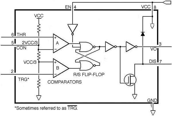
FIGURE 1. Internal circuitry of the timer.
Comparator A’s positive input is brought out on the threshold THR, pin 6, and comparator B’s negative input is brought out as the trigger TRG, pin 2. The comparator outputs are fed into digital logic in the form of an RS flip-flop that remembers the comparator’s output transitions. Bias currents on these inputs are quite small; on the order of nanoamperes (nA).
A discharge MOSFET DIS, pin 7, is also provided to rapidly discharge the capacitor in the tank circuit. The drain of this FET is reverse biased by a diode attached to Vcc to prevent people from using the open drain with a pull-up resistor to a voltage greater than Vcc. The enable input EN, pin 4, when taken low (i.e., 0 volts) resets the flip-flop and locks the timer output VO, pin 3, low, (i.e., 0 volts). EN, also called “reset” or “not reset” is seldom used, but has some special uses as discussed herein.
The Timer as a One-Shot
Take a look at Figure 2. The monostable or “one-shot” connection of the timer enables the flexible generation of single pulses of durations ranging from about one microsecond to one second.
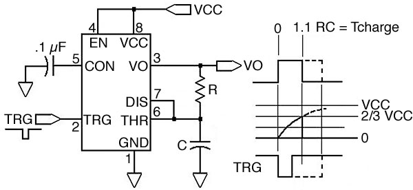
FIGURE 2. The timer in monostable or “one-shot” mode.
At first glance, this capability might seem of questionable value, since the user is required to generate a triggering pulse of duration somewhat less than the output pulse itself. Considering however that the output pulse is a clean square wave that can be made stable with variations in temperature and rail voltage, the advantages become more apparent. Further, the pulse duration is easily tailored by selection of the RC tank, and the output, Vo, has a considerable ability to source and sink reasonable loads. Sourcing is at least 10 mA and sinking currents range upward to 100 mA.
In this form only, note that alternatively, R can be connected to Vcc instead of Vo, with Vo being entirely free except for external loads. This is an older connection form that is a remnant of when timers were fabricated with bipolar technology.
Figure 2 shows the connections necessary for monostable operation. Here, the threshold and trigger inputs are separated, with a negative-going pulse on the trigger being the initiating stimulus. Input THR (threshold, pin 6) is still attached to the capacitor, and DIS is attached to C also. The essential triggering rule specifies that the triggering waveform (pin 2) must recover above the lower threshold of Vcc/3 before the capacitor in the RC tank achieves the “time-out” threshold voltage of 2Vcc/3 — and since the output pulse is high while the capacitor is charging from 0 volts to 2Vcc/3, a little mathematics shows that the output pulse duration, Tcharge, is given by:
Tcharge = 1.1 x R x C
Example: We want to generate an output pulse of one millisecond duration, and accordingly choose R = 90.9K, and C = .01 µF, producing a nominal pulse of one millisecond ±10 %.
Tcharge = 1.1 x R x C = 1.1 x (90.9 x 103) x (1 x 10-8) = 1 x 10⁻³ seconds
When Tcharge ends, the internal MOSFET servicing DIS rapidly discharges the capacitor and prepares the timer for another triggering pulse. Since the “on-resistance,” Ron, of the MOSFET is specified at 40 ohms maximum, we should allow some recovery time, Trecover, to drain the capacitor before retriggering.
Trecover = 4 x 40 ohms x C
Using this formula, we should allow 1.6 microseconds for a capacitor value of .01 µF, before re-triggering the timer.
Triggering Rules
Many of the problems encountered by beginning timer users are related to triggering. As shown in Figures 1 and 2, the timed output Vo is made to go high when the voltage on the /TRG (read as “not trigger”) is taken below Vcc/3. This causes the lower comparator to transition to a logic 1 (high), which sets the RS flip-flop. The capacitor starts charging at ground, having been discharged and clamped there by the internal MOSFET accessible as DIS on pin 7.
The change in the output state of the flip-flop turns off the MOSFET, and Vo begins to charge capacitor C through resistor R. The numerical product, RC, is the time constant that applies to this charging, and the capacitor voltage rises in a diminishing exponential curve. This voltage passes upward through the lower threshold without changing the state of the flip-flop until it reaches the higher threshold of 2Vcc/3. This charging occupies 1.1 time constants (i.e., 1.1RC) of the tank circuit and
determines the duration of the Vo output pulse, Tcharge.
Looking at the internal logic, we can see that the /TRG waveform must return to its normal high level before the capacitor reaches the upper threshold — otherwise, as shown by the dashed lines at the Vo and /TRG waveforms, output Vo will “hang” and not transition to low. This is the basis for the previously cited triggering rule. Thus, the pulse width of /TRG from the initiating processor or other logic must be kept reliably less than the desired output pulse width.
Note that the upper node of the divider is brought out on the control pin. This pin is seldom used, even by seasoned designers. Strictly speaking, CMOS timers do not require a decoupling capacitor attached to CON, but I never miss an opportunity to decouple DC networks, and I recommend .1 µF as shown to achieve additional filtering of Vcc.
Generating the Trigger Pulse in the One-Shot Mode
Figure 3 shows two ways of generating a triggering pulse for monostable operation. The first (“often used”) employs an RC trigger network (Rtr and Ctr) with a recovery clamp diode to generate a pulse from the falling edge of a square pulse.
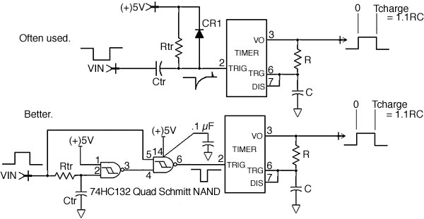
FIGURE 3. Generating trigger pulses for the one-shot timer.
This method incorporates the liability of all differentiating networks — sensitivity to outside noise, conducted or radiated into the circuit by infrequent, spurious events. This can produce unwanted triggering. On the other hand, it generally does not require extra logic gates to implement. Notice the small positive spike when Vin rises and the clamp comes on.
The triggering waveform recovers upward to Vcc/3 in a time given by .4 x Rtr x Ctr. Thus, to conform to our triggering rule, we must keep the recovery time less than 1.1 x R x C of the tank circuit.
Keep Rtr x Ctr < (1.1 / .4) x R x C, or
Rtr x Ctr < 2.75 x R x C, so that
RtrCtr < RC is a safe rule, and allows generous component tolerances.
The second method (see “better”) generates the trigger pulse using an integrating network. This method is more likely to be used by careful designers; it works well and has inherent noise rejection. Two Schmitt NAND gates generate a trigger pulse from the delay in the charging of Ctr, by currents through Rtr. Besides establishing the trigger’s pulse width, the Rtr and Ctr combination acts as a low-pass filter that rejects spurious noise. The “safe” triggering time constant for this method differs from the “often used” form: There is much less margin. So a reasonable rule that allows for component tolerances requires:
Keep RtrCtr < .4 RC.
The Timer as a Free-Running Oscillator
The timer in free running (or astable) mode becomes a digital oscillator. In Figure 4, we see that the threshold (pin 6) and trigger (pin 2) inputs have been externally connected to form a single input into both comparators.
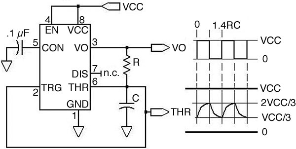
FIGURE 4. The timer in astable mode.
The output Vo performs double duty by alternately charging and discharging C through R. Since the voltage on C is connected to the trigger and threshold inputs and responded to by the comparators, the feedback loop is thereby closed, and oscillation is sustained. Take a little time to reason your way through how the logic responds to the comparators to generate the output Vo.
The exponential charging and discharging waveform of the capacitor is, of course, trapped between the trigger and threshold pins, and the total time required to alternately charge and discharge the capacitor defines the period of oscillation — the reciprocal of which is the frequency. As shown in Figure 4, the charging and discharging of the capacitor within the threshold window consumes 7/10 of a time constant of the RC network. And since both operations determine the period (Tperiod) of oscillation, we have:
Tperiod = Tcharge + Tdischarge = (.7 x R x C) + (.7 x R x C) = 2 x (.7 x R x C) = 1.4 RC
and the frequency = 1 / Tperiod = 1 / 1.4RC
Using our previous values of R = 90.9K ohms and C = .01 µF, we arrive at Tcharge = Tdischarge = .636 milliseconds and Tperiod = 1.27 milliseconds.
Frequencies from about 1 Hz to 1 MHz can be reliably produced in this mode. The lower limit is set by the capacitor leakage current relative to the charging current. The careful designer will resist the temptation to realize frequencies below about 1 Hz (i.e., periods greater than one second) directly from the timer by employing large values of R and C. Rather, one should apply some kind of “divide-by-N” counter to Vo or a series of flip-flops to achieve longer periods. Otherwise, instability with temperature and time relating to the RC tank circuit will usually plague what at first looks to be a good result. Capacitors above one microfarad will typically be tantalum or aluminum electrolytic selections with leakage many times greater than film capacitors at one microfarad or below.
With the above in mind, the following approximate limits on R and C will prove to be helpful.
5K ohms <= R <= 2 megohms
Use a 1% tolerance metal film resistor, leaded or SM, 100 ppm/C or less.
20 picoFarads <= C <= 1 microFarad
Tolerance 5%, film, use polymer, X7R or NPO dielectric.
For C > 1 µF, compute the capacitor’s leakage at Vcc and compare it to the minimum charging current. When selecting a tantalum or aluminum electrolytic capacitor, you can minimize this leakage by choosing a unit with a substantially higher working voltage than Vcc. I often use capacitors with a rating of 35 VDC working voltage.
The upper limit on frequency is set by the speed of the integrated circuit itself. This is specified at 1 MHz in the astable mode. But in the one-shot mode, note that Trecover (the recovery time) limits the pulse repetition rate.
Tolerances on Frequency
One of the strengths of the timer is that the duration of the output pulse, Tout, is largely invariant with typical changes in Vcc because the timing is determined by the fixed ratio of the upper and lower threshold resistors which are, in turn, driven by Vcc. Interestingly, this invariance is true, even though the charging is nonlinear, because the charge scaling is completely maintained.
However, diffusion processes for the internal resistors limit fabrication of the resistor ratios to about ±2% accuracy. I allow a total of ±5% inherent timer accuracy. Also, allowing for component tolerances as previously recommended, we arrive at a probable error of ±7.1% RSS (root-sum-square) and a maximum timing error within ±11%.
Temperature stability of the timer input is typically within ±100 ppm/C. Allow another 1% timing error for aging during the first 1,000 hours of use, after which the unit should be essentially stable.
Varying the Duty Cycle of the Astable Oscillator
Look at Figure 5. A variation on the RC tank circuit enables the user to set the duty cycle greater than 1/2 for the astable timer. Here, we shorten the discharge time by the addition of resistor Rdischarge.
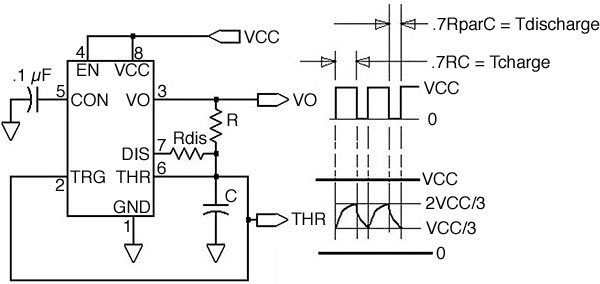
FIGURE 5. Shortening Tdischarge independently of Tcharge in the astable mode.
The astute reader will note that charging occurs solely through R, while discharging occurs both through R and Rdischarge. Thus:
Tperiod = Tcharge + Tdischarge = .7RC + .7RparC
where Rpar is the parallel
combination of R and Rdis, derived as:
Rpar = (R x Rdis) / (R + Rdis)
Again, continuing our example with the previous values, let’s shorten Tdischarge to .32 milliseconds. To do this, choose Rdischarge = 90.9K.
Tcharge = .7RC = .636 milliseconds (as before)
Rpar = (90.9 x 10³)(90.9 x10³) / (90.9 x 10³ + 90.9 x 10³) = 45.45 x 10³ ohms. Choose the nearest MIL decade value of 45.3K ohms.
Tdischarge = .7 x 45.3x103 x 1 x 10-8 = .317 milliseconds
Tperiod = .636 milliseconds + .317 milliseconds = .953 milliseconds
Frequency = 1 / Tperiod = 1.05 kHz
Duty cycle, d, is defined as = Tcharge / Tperiod = .67
Changing Tcharge and Tdischarge Independently of Each Other
This is more involved. Figure 6 shows a method for this that requires some extra transistors, but does not degrade the temperature stability of the circuit, as popular diode approaches definitely do.
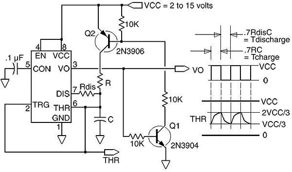
FIGURE 6. Changing Tcharge and Tdischarge independently.
Here we have Vo drive two saturated switches Q1 and Q2. Q2 connects Vcc to tank resistor R only during the charge time when Vo is high, and the discharge FET at DIS, pin 7, is off. No current flows through Rdis during Tcharge. During the discharge time, no current flows through R, but only through Rdis. This makes Tcharge and Tdischarge independent of each other.
Using the ENABLE Function
As shown in Figure 7, EN, pin 4, when taken low, forces Vo low by resetting the RS flip-flop. This does not appreciably reduce the timer’s quiescent power, but prevents TRG and THR from functioning.
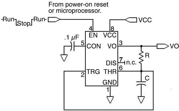
FIGURE 7. Using the enable function EN.
EN in the one-shot mode can be used to terminate a pulse in progress, but is otherwise not particularly useful since the timer remains inactive unless triggered anyway. In the asynchronous mode, EN can be used by a microprocessor to initiate or terminate oscillation, but note that the initial Tcharge time will be longer (= 1.1 RC) than any succeeding charge times (= .7RC) because the capacitor starts at zero volts, but later is trapped between Vcc/3 and 2Vcc/3.
EN is often used as a power-on reset, being held low by a special reset circuit when power is first applied, and remaining there until all circuitry (including the microprocessor) is live and settled. There are other techniques for using EN, but these will not be covered here. Check out manufacturer’s application notes.
Conclusion
In the various figures, no output logic buffers have been shown for Vo for simplicity. Isolating Vo by buffering is always a sound procedure and I recommend it. This insures that small variations in Vo due to variable external loads do not affect the tank charge or discharge times.
Finally, remember to observe all precautions to avoid electrostatic damage when storing and installing the part. CMOS static damage is often latent, showing up only weeks after the damaging shock has occurred. However, once the timer is soldered safely into the circuit, it is difficult for it to experience electrostatic damage because of distributed circuit capacity.
I suggest that you keep several timers such as the TLC555 on hand. You never know when you might need a tailored square wave or pulse in your design — and your microprocessor will thank you for the outside help! NV