Working with Field Programmable Gate Arrays (FPGAs) — Part 1
Go back over 30 years — during the early years of the 1990s, electronics hobbyists and even professional engineers were getting excited by the prospect of using microcontrollers in all kinds of projects. These ICs could be programmed in assembly language to perform a wide variety of tasks under program control and the possibilities seemed endless.
Initially, microcontrollers were only available in an erasable programmable read only memory (EPROM) form where stored programs could be erased by exposing microcontroller ICs to ultraviolet (UV) radiation for a few minutes. Once erased, a new program could be downloaded into the IC through a serial (RS-232C) cable connected to a PC. By the turn of the century, microcontrollers based on Flash memory technology were introduced which greatly simplified the repeated program/erase cycles needed during application development.
This greatly enhanced the appeal of microcontrollers and they started appearing in so many applications that to find an electronic system without one or more microcontrollers became a challenging task in itself.
Eight-bit microcontrollers gave way to 16- and even 32-bit devices for increasingly demanding applications. Come 2017, and microcontrollers are firmly established as the brains behind almost every system requiring some amount of intelligence.
Today’s microcontrollers are highly integrated system on chip (SoC) devices that bundle together many useful peripherals with the processor, and allow designers boundless possibilities. Given this state of development, it’s not surprising that microcontrollers are now thought of as the ultimate control devices with no need for any other approach for implementing digital control and processing functions.
It may then come as a surprise to know that an increasing number of digital systems are now being implemented with a diametrically opposite ‘pure hardware’ approach. These are based on programmable logic ICs that can perform any function that a microcontroller can (and more), without actually executing a stored program. Modern programmable logic devices have had their own evolution — separate from the track followed by microcontrollers. This is an involved story in its own right, but suffice it to say that, over the years, programmable logic devices have developed greatly in complexity and capability.
FIGURE 1. Intel’s high-end Stratix V FPGA. (Courtesy of Intel Corporation.)
Modern programmable logic devices (Figure 1) principally belong to the class of field programmable gate arrays (FPGAs). Despite having programmable in their name, FPGAs and other such programmable logic devices are not programmed in the usual sense of the word, as is applied to microcontrollers. Here, programming the device refers to configuring the inner circuitry of the chip to make it capable of performing one or more digital functions.
This is a very powerful concept that deserves a look in greater detail, so persevere and read on, and you will be rewarded with the appreciation of great new power by the end of this two-part series.
A movie on a DVD can be watched on two separate devices. We can pop the DVD into a DVD player or use the CD/DVD reader that comes with PCs and laptops. Either approach will enable us to view the movie, but the DVD player will probably provide the better viewing experience. On a computer, the movie may play erratically with the processor sometimes struggling and the cooling fan coming on frequently.
This disparity arises because of the different methods employed by these two devices to play a DVD. A sequentially executing program in computers handles the task of decompressing the raw data stream coming off a DVD and making it presentable for the device screen. The sequential instruction execution methodology necessarily slows things down so limits to performance are quickly reached. The computer’s processor really has to struggle to keep up with the rapid stream of 1s and 0s arriving from the disk reader.
In contrast, a DVD player makes use of application specific chips (ASICs) for performing DVD read and display tasks in real time without the use of a single line of code. Many tasks can be executed in parallel, i.e., together in time which endows this scheme with limitless power.
Thus, there are two clearly distinct ways of performing any digital task: using a stored program processor; or using an interconnected arrangement of logic gates that process digital data in real time. FPGAs are used for the latter and are akin to ASICs; albeit ones that you can design yourself to perform almost any digital task that you can think of.
Once properly configured, an FPGA becomes a specialized IC with a known behavior of its I/O pins. Digital data can enter and exit this IC at designated pins, and it will be processed in accordance with the design configured inside the chip. Application development is similar to that with microcontrollers — you can load a configuration, debug it, modify it, and re-load it until you get the desired functionality.
What advantages do FPGAs provide over traditional processors in demanding applications? This is a vital question, and its answer shines light on why FPGAs are increasingly proliferating in electronic equipment these days.
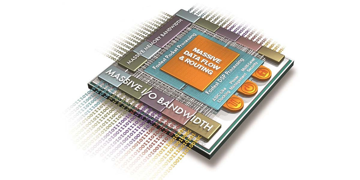
For starters, programmable logic devices are capable of working at much higher clock rates than eight- and even 32-bit microcontrollers. Inexpensive FPGAs easily clock at 200 to 300 MHz, and more specialized devices such as the UltraSCALE™ products from Xilinx (see Figure 2) can handle clock frequencies close to a GHz. This brings with it raw power which is even more magnified when one realizes that FPGAs do not require so many clock cycles to execute algorithms as processors do.
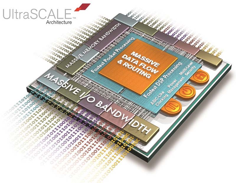
FIGURE 2. Xilinx UltraSCALE FPGAs are built using advanced chip-making technology for demanding system-level digital applications. (Courtesy of Xilinx, Inc.)
Instead, they are simply an interconnection of gates, transforming bits and bytes on-the-fly in real time. Thus, complicated algorithms that require many instructions can be profitably implemented in an FPGA, where processing is only limited by the propagation delay of logic gates (and a small overhead from gate interconnections). These features can and do make FPGAs blazingly fast when compared to microcontrollers.
Another advantage that FPGAs have over microcontrollers is in the sheer profusion of I/O pins they have. Whereas a typical microcontroller may give you 20 to 30 I/O pins, even a low-end FPGA typically provides around 50 I/O pins. Larger FPGAs sport hundreds of pins (see Figure 3), so you almost never run out of connectivity with the external world.
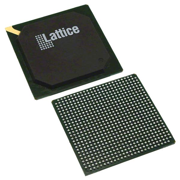
FIGURE 3. Top and bottom of a ball grid array (BGA) FPGA package showing large numbers of mainly I/O pins. (Courtesy of Lattice Semiconductor Corporation.)
As an aside, the large number of pins means that FPGAs come in advanced multi-pin packages such as high pin count quad flat packs and dense ball grid arrays. This makes it difficult to solder them to PCBs (printed circuit boards), but as we will see in Part 2, there are ways around that.
Added to that is the flexibility with which one can use the I/O pins. Thus, one set of pins can handle signals at 3.3V logic levels, whereas another set handles signals at 2.5V or even 1.8V. You can mix and match I/O banks such that it is easy to perform logic level translation from one standard to another. Note that 5V logic levels are usually not supported on current FPGA chips.
Yet another attractive feature of FPGAs is the large amount of logic resources they make available at very reasonable costs. Even a small FPGA costing about $5 comes with the logic equivalent of tens of thousands of gates. Larger devices easily give you access to millions of gates inside a single chip. The logic resources can, of course, be interconnected (configured) in any way you like to realize almost any digital function; be it as simple as a basic AND-OR-NOT logic expression or an entire Ethernet controller.
What is more, given the large number of I/O pins and logic elements, you can put a lot of completely different digital designs in a single FPGA. This is very useful where one wants to consolidate a number of different digital ICs into a single physical package. This approach saves money and space, making systems smaller, lighter, and cheaper. Logic consolidation is a big reason for the increasing sales of FPGAs for commercial, industrial, and military products.
Finally, over time, FPGAs have grown into veritable SoCs so that other useful functions (besides just an array of uncommitted logic elements) now come integrated on the chip. Commonly available features include phase locked loops (PLLs) for generating almost any frequency on a chip, embedded memory blocks, fixed (and even floating point) multipliers, and analog-to-digital converters (ADCs), etc.
High-end FPGAs also feature integrated high speed serial data transceivers. Using these integrated functional blocks with user defined logic, one can build extremely complex digital systems on a single chip.
When first introduced, FPGAs may look daunting. How do you go about building useful systems with something that is basically just an array of logic elements? It turns out that this is simpler than one might imagine. You can certainly use a gate-level circuit diagram for simple circuits, but that will probably not end up using even 1% of the logic resources available in modern FPGAs. Proper utilization of the power of FPGAs demands a radically different approach to describing circuit behavior.
The secret lies in using a hardware description language (HDL) to describe the desired functionality. There are several of these around but two — VHDL and Verilog — are, by far, the most common HDLs; they are employed by 99% of FPGA users around the world. Here is the fun part — an HDL allows a developer to describe the desired system in a high-level form without worrying about its exact implementation in terms of logic gates. That is the function of the HDL compiler, which takes the design code and generates a circuit design in the form of a net list.
This describes the interconnections between FPGA logic elements that would let the device — or more commonly — a part of the device be configured to perform the desired task. The net list comes as a compiler-generated output file, usually called an SRAM object file (SOF) that can simply be downloaded into an FPGA using a USB cable — much as a hex file can be downloaded into a microcontroller.
With this approach, the developer does not need much knowledge of gate-level digital design or even the architecture of the FPGA, as the HDL compiler takes care of all that. Thus, as soon as one learns either VHDL or Verilog, great design capabilities open up.
Both languages are highly regulated IEEE standards, with VHDL more common in Europe while Verilog is more prevalent in North America. The latter is perceived as easier to learn whereas the former is more verbose. However, on the whole, both provide the same capabilities.
This article will illustrate examples using VHDL in Part 2, but the basic ideas can be implemented in the same way using Verilog. Once a design has been processed by an HDL compiler, it can be converted to a design block (usually called an intellectual property block, or just IP) which can be used as a stand-alone component in any subsequent design. In this way, a complex design can be made up by simply connecting a number of simpler IP blocks that have been separately designed and tested.
This hierarchical design methodology is very powerful and allows designers to build very sophisticated systems relatively easily. IP blocks are also made available by FPGA manufacturers to support their products. Customers can make use of them by incorporating them in their own designs. As an example, a floating point multiplier IP can take two binary words and give out their product. Using such a block frees the designers from doing all the hard work of creating this functionality themselves. There is a good market for third-party IPs with specialist companies selling or licensing their design blocks for use with many FPGA families.
It is the general practice with FPGA users that a digital function that is hardwired inside an FPGA is called a hard IP, whereas one that is implemented through HDL code is called a soft IP. An entire microcontroller — such as a 32-bit ARM processor — can be found as a hard IP on certain FPGAs, whereas it could also be implemented as an HDL-described element.
Soft IPs use up logic resources on FPGAs, leaving less for implementing other HDL-defined functions. Hard IPs are already integrated on FPGAs, so their use does not consume any configurable logic resources on the chip. Because they are highly optimized and functionally verified by the chip manufacturer, they should be used where possible instead of using custom-written HDL code.
Strictly speaking, designing with FPGAs does not require an in-depth understanding of their chip-level architecture. However, some understanding is needed to appreciate how a design gets ‘placed and routed’ inside an FPGA. Unlike processors which may have anywhere from one to eight processing cores (sometimes even more), FPGAs are highly granular. These devices are made up of a dense array of logic blocks (LBs), also called logic array blocks (LABs). Instead of simple logic gates, the LBs are the smallest unit of functionality in FPGAs.
Each LB usually consists of a look-up table (LUT) and a flip-flop (FF). An LUT is typically a 4-to-1 multiplexer with inputs tied to known logic levels. This arrangement acts as an AND-to-OR combinational logic element, with the output determined by the selection input fed to the multiplexer. The LUT output can go to the output of the LE directly or through a clocked D-type FF. The latter ensures that sequential circuits could also be implemented.
Generally, real LBs are quite a bit more complex than this description, but the main idea of LUTs followed by FFs is almost universal. The LBs are arranged in a two-dimensional array with interconnection wiring running between them. This is so cleverly laid out that any LB can share its output with any other LB on the chip. The dense interconnection circuitry is often called the FPGA ‘fabric.’ The configuration net list file mentioned earlier serves to control transistor switches in the fabric that interconnect or ‘route’ selected LBs together.
Each transistor switch is implemented as a single SRAM cell making the FPGA look like a distributed bit-level memory. Thus, an FPGA design in an SOF file is nothing more than an SRAM array bit pattern. This serves to switch on some interconnection transistors while keeping others switched off; this creates an LB-based circuit that performs the designer’s bidding. Figure 4 shows a high-level architectural overview of an FPGA device showing the layout of LBs, interconnection fabric, I/O blocks, and PLLs.
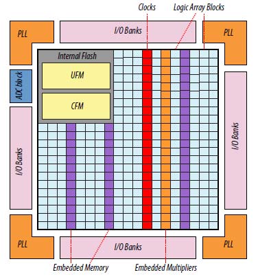
FIGURE 4. Intel’s MAX 10 FPGA architecture. (Courtesy of Intel Corporation.)
The fact that most FPGAs are based on SRAM technology means that — just as SRAM chips — they lose their configuration information if power is switched off. This makes them volatile and necessitates the use of an accompanying Flash memory that could feed the FPGA with its configuration file each time the system’s power is turned on.
Serial Flash memories performing this role are called configuration memories or configuration devices. On power-up, FPGAs look to download their configuration data from a nearby Flash memory. This process only takes a few milliseconds, and then the FPGA starts behaving in the intended manner.
While the vast majority of FPGAs are exclusively SRAM based, a small minority have an on-chip Flash memory block where configuration data can be stored. On power-up, such FPGAs tend to read the internal Flash memory and use its content to program the SRAM cells in the FPGA fabric. This feature removes the need for a separate Flash memory device to hold configuration data. Altera’s MAX 10 family and Microsemi’s IGLOO family (see Figure 5) are examples of this type of Flash FPGA.
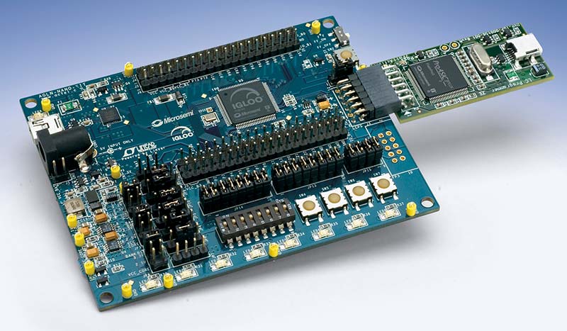
FIGURE 5. Microsemi IGLOO FPGA development board. (Courtesy of Microsemi Corporation.)
Only a little more needs to be said before we wrap up this discussion of FPGAs. In order to provide maximum flexibility and performance, most FPGAs require multiple supply voltages. For instance, a typical FPGA may require both 3.3V and 1.8V regulated DC supplies, rated at more than one amp each. Some devices may require three or even four different supply voltages.
On the other hand, there are also FPGAs that can be operated in a single supply mode, though with some loss of performance. While this might appear as a nuisance, a big advantage of the multiple voltage scheme is that FPGAs can work with almost any logic level family and can also convert from, say, 3.3V CMOS to 1.8V CMOS logic very easily.
Finally, like most other digital ICs, FPGAs too require a clock source to synchronize internal operations. There are dedicated I/O pins on all FPGAs that accept clock signals from off-chip oscillators. These pins connect to clock distribution networks inside FPGAs, through which the clock signal can be brought to every LB on the chip. Thus, just like microcontrollers, FPGAs also require an external oscillator to function.
Additionally, all modern FPGAs have one or several PLLs that can take the external clock signal and generate derived clocks that are desired multiples of the input frequency. This way, the frequency can be increased or decreased to suit a given application.
This brings us to the end of Part 1. In Part 2, we will take a look at VHDL as an HDL for implementing designs in FPGAs; examine some commercially-available FPGAs and FPGA development boards; see how one can incorporate FPGAs in real designs; and describe a simple FPGA code example in VHDL. NV