Working with Field Programmable Gate Arrays (FPGAs) — Part 2
In Part 1 of this two-part series, we looked at the basics of programmable logic: the structure of FPGAs and their utility in digital system design. In this concluding part, we’ll explore how FPGAs are actually used. This takes us into hardware description languages (HDLs) used for configuring programmable logic devices, and the hardware/software environment used for application development.
Superficially, designing a digital circuit in an FPGA looks similar to programming a microcontroller. You write code that looks and feels much like writing code in any high level computer programming language. VHDL code specifically bears a strong resemblance to the software programming languages PASCAL and Ada, because of historic reasons.
VHDL is an abbreviation that contains another abbreviation inside it. VHDL stands for VHSIC Hardware Description Language, with VHSIC standing for Very High Speed Integrated Circuit.
The names have only historic significance, but what is really important while writing VHDL (or Verilog) code is to keep in mind that you are writing the design description for a digital system, not sequential instructions for execution on a processor. This is in spite of the fact that HDLs contain similar constructs as do ordinary software programming languages (assignment statements, conditional expressions, loops, etc.)
Making a Statement
In the case of an HDL, these statements reflect the way the desired system is supposed to behave. The HDL compiler makes use of the statements to work out the circuit configuration needed to accomplish the desired functionality. As a very simple example, a conditional expression written in VHDL as
out_clk <= in_clk when ((bit1 AND bit2) = ‘1’);
(which gates a clock signal) is equivalent to the circuit layout shown in Figure 1.
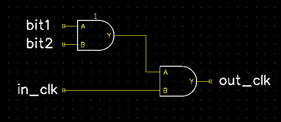
FIGURE 1. Gate-level schematic; equivalent to a typical conditional statement in an HDL.
HDL code is said to be written at the behavioral level, i.e., it is written by the developer in a way that describes the intended circuit function rather than as a circuit description. The latter is derived from the former by the HDL compiler.
Technically speaking, the compiler is said to ‘infer’ circuit elements by looking at the way HDL statements have been written. Thus, a simple assignment statement such as z <= a + b; is enough for a VHDL compiler to infer the need for an adder circuit. This way, a designer can focus on the task at hand rather than how to implement it in hardware.
Here, you can see the power of an HDL based approach to logic design; gone are gate and flip-flop level logic designs, Karnaugh maps, and logic minimization. Instead, one need only describe the pin-to-pin functionality employing easy-to-use HDL statements.
Some of these statements are sequential; that is, they signify operations that are performed one after the other. Other statements are concurrent in nature, i.e., in the hardware, they execute together at the same time. Concurrent statements are a hallmark of HDLs; software programming languages only have sequential statements.
HDLs need concurrent statements because — by their nature — hardware works in parallel in real time, so their descriptions require the ability to express simultaneous circuit behaviors. Understanding concurrent versus sequential statement execution is often the biggest challenge in mastering HDL coding.
Getting Real with Code
Let’s look at some real code for configuring FPGAs. The basics are logical (oh!) and not difficult to understand. In VHDL, a digital system is described using two separate but interlinked design units. The first (called an ‘entity’) describes the desired system’s I/O interface; that is, all signals coming in and going out of the system. This part regards the system as a black box and pays no attention to the function or structure of the system. That comes next in the ‘architecture’ unit.
That is where you describe the system’s functionality. That’s all. An entity architecture pair can be compiled by a VHDL compiler to generate a circuit net list as a .sof file. This is easier to show with an example:
library ieee;
use ieee.std_logic_1164.all;
entity counter is
port (clock : in std_logic;
new_clock : out std_logic);
end entity;
architecture design of counter is
signal temp_clock : std_logic;
begin
process (clock)
variable count : integer;
begin
if (rising_edge(clock)) then
if count < 500 then
count := count + 1;
else
count := 0;
temp_clock <= not (temp_clock);
end if;
end if;
new_clock <= temp_clock;
end process;
end design;
This simple (and working) example shows VHDL code for a clock divider that divides the frequency of a square wave clock by a factor of 1,000. All VHDL reserved words are in bold letters. This self-contained piece of code is highlighted to show three main sections: compiler directives; entity declaration; and architecture definition. Let’s go over the code to see how everything is supposed to work.
Working It
The first two lines make the VHDL compiler include an IEEE standardized library with many essential definitions for use in the compilation process. These lines are always included in VHDL code that is fed to a compiler (note that we never say VHDL or Verilog program). The next few lines declare and define an entity that has been named ‘counter’ by the code writer. Any name (allowed by identifier naming conventions) can be used.
In the entity part, you show the I/O of the system within the keyword port. Here, two signals (clock and new_clock) have been declared. The first signal enters the system from the outside and is thus of the type (or in VHDL parlance, mode) ‘in’ whereas the second signal goes out of the system and is, therefore, of the mode ‘out.’
Any number of in and out signals can be included in the port part. The mode can also be ‘inout,’ which stands for a bidirectional signal. Here, the signals are std_logic which essentially means they can represent a single bit such as 0 or 1 (or even a high impedance state: Z). Multi-bit vectors that represent bytes and words will be of a type such as std_logic_vector (7 down to 0).
Just as in software programming languages, comments can be included in VHDL code. These are preceded by two dashes, after which the rest of that line is treated as a comment line.
The inner workings of the system are given in the architecture design unit. The architecture is given its own name (design, here) of the coder’s choice. The architecture is bracketed between its begin and end keywords. Before begin, any number of variables and/or signals can be declared for local use inside the architecture body (such as the temp_clock signal).
Inside the main architecture body, a special VHDL construct called process has been used. It can have its own local variables such as the variable count integer seen here. A process is essentially a block of code that gets activated whenever the signal (or signals) that appears in the bracket after the keyword process change in value (say, from 0 to 1 or 1 to 0).
These signals are called the sensitivity list of the process. Here, there is only one signal clock in the sensitivity list of our process. Each time the clock transitions from 0 to 1 or vice versa, the code in the process block operates. If the clock transition is from 0 to 1 (a rising edge), then the lines underneath are executed.
In this part, the value of the variable count is checked. If it is less than 500, then it is incremented by 1. This happens for 500 consecutive process activations (500 rising edges of the clock). After 500 times, the else part is executed once, where the count is reset to 0 and the value of the signal temp_clock is toggled (1 becomes 0; 0 becomes 1). For 500 rising clock edges of the input clock, the temp_clock signal remains 0 or 1 and then toggles to the opposite state for the next 500 time periods of the clock input. This way, temp_clock becomes a ÷1000 version of clock.
Toward the very end of the process, the value of temp_clock is assigned to the output signal new_clock which — from the outside — is seen as toggling at 1/1000 of the rate of the input signal clock.
An architecture can have any number of process blocks — each with its own sensitivity list of signals. All processes operate in parallel (concurrently) with each other and thus can be regarded as separate small components. They can communicate with each other if needed, using signals declared in the declarative part of the architecture (before the architecture’s begin keyword).
These signals are visible throughout the architecture (as are signals that appear in the port list). Note that new signals cannot be declared inside processes, but variables can be declared in the declarative part of any process (before the process begin keyword). Such variables can be used inside that process alone. These variables retain their values between process executions and thus can be used for counting, etc., as illustrated above.
Short and Sweet
Although short, this example shows what VHDL code looks like, how it is structured, and how it works. Note that we did not actually describe a conventional counter based digital design. The VHDL compiler will infer a counter from this description and implement the net list for a logic element based counter circuit with signal input and output called clock and new_clock, respectively. This code can be compiled by any VHDL compiler to produce an FPGA configuration file.
It is also possible to actually see the circuit configuration that will be implemented inside an FPGA. To do this, one can invoke the schematic viewer built into HDL compilers. A part of such a schematic layout (not for the code illustrated here) is shown in Figure 2.
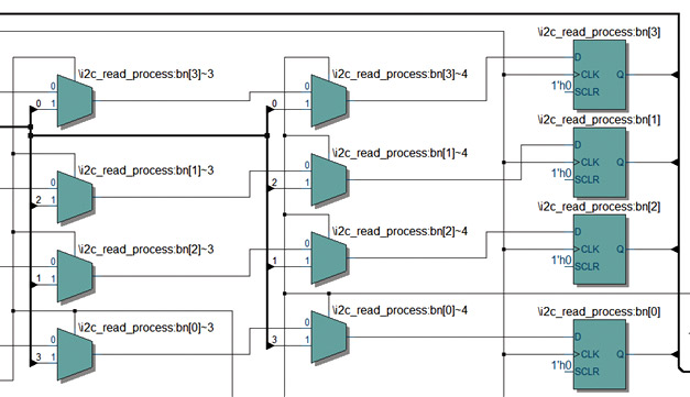
FIGURE 2. Typical interconnections inside an FPGA implementing a user-defined circuit.
One last thing that needs to be done before the configuration file is downloaded to the FPGA is to assign physical pins to the signals declared in the entity’s port. In the example above, both signals are one bit and thus will need one I/O pin assigned to each.
The compiler assigns arbitrary pins to port signals during the compilation process. These can be changed to the user’s chosen pins after compilation. The code is then compiled once again so that the new pin assignments get embedded in the output file. After that, it is a simple matter of downloading the configuration file over a USB or Ethernet interface to an FPGA through a JTAG interface.
Once that is done, the FPGA assumes the personality ascribed to it through the user’s configuration code. From that point on — unless its configuration is altered — it is essentially a function-specific digital IC that you designed yourself.
Why FPGAs?
What are FPGAs used for in preference to microcontrollers? There are several answers to this question. Logic consolidation (where one replaces a number of digital ICs with a single IC) is a big reason for using FPGAs. Due to the large number of logic elements (LEs) and I/O pin resources in an FPGA, a number of functions can be placed inside the same FPGA. For example, an ADC controller, a number processor, and a display driver (among other functions) can be placed inside an FPGA. Many commercial products use FPGAs in this way to make products smaller, lighter, and cheaper.
Transmission protocol conversion (USB-to-serial, serial-to-Ethernet, I2C-to-SPI, etc.) and logic level translations are other commonly encountered functions that are frequently performed with FPGAs. The fast and deterministic (known timing delays) nature of FPGA circuits makes them especially suitable for these duties.
Due to the high speed with which FPGA implementations can work, FPGAs are often used to remove the processing load from processors. Specialized processing such as fast Fourier transforms (FFTs), floating-point operations, digital filtering, etc., can be efficiently carried out in FPGAs, leaving the main processor in a system to execute the main thread of program flow, respond to interrupts, etc.
Stored program processors are eminently suitable for carrying out a set series of instructions repeatedly. FPGAs can off-load them from carrying out complicated algorithms that will take a very large number of program instructions to execute.
The combination of a traditional processor and a programmable logic device can be very powerful and is one that is often seen in many types of defense, avionic, industrial, and medical equipment. Another scenario where FPGAs are usually employed is seen when a certain operation has to be performed in parallel on a large number of different data bytes or words. This often happens in video processing and scientific vector calculations.
Yet another situation where FPGAs have a definite edge over processors running software is where large arrays have to be scanned quickly. Cameras and displays can both use FPGAs with their large number of I/O pins to quickly scan arrays and columns in order to acquire or display images.
Making FPGAs
Today, FPGAs are mainly manufactured by a handful of semiconductor companies. Xilinx, Altera, Lattice Semiconductor, Microsemi Corporation, and Cypress Semiconductor form the list of main US FPGA suppliers (in order of market share). Over a year ago, Altera was acquired by Intel Corporation, so that it is now a part of Intel’s business. This large acquisition underscored the importance of programmable logic in today’s electronics.
Each company has its own line of FPGA offerings which range from relatively small (and cheap) ICs to very large devices with millions of LEs and hundreds of I/O pins. Not surprisingly, FPGA prices vary widely from just a few dollars each for small devices, to hundreds and even thousands of dollars for top-of-the-line chips.
A visit to the websites of FPGA manufacturers is highly recommended as that is where they showcase their new as well as established products, and describe their features and capabilities in detail. Smaller FPGAs, such as those in the Spartan family from Xilinx and the Cyclone family from Altera (Intel) are very suitable for use by hobbyists. Many easy-to-use development boards are available that contain an FPGA together with other useful devices, such as memories, ADCs (not all FPGAs contain analog-to-digital converters), clock oscillators, etc., in addition to a few switches, LEDs, and seven-segment displays. These development boards range in price from less than a hundred dollars to thousands of dollars.
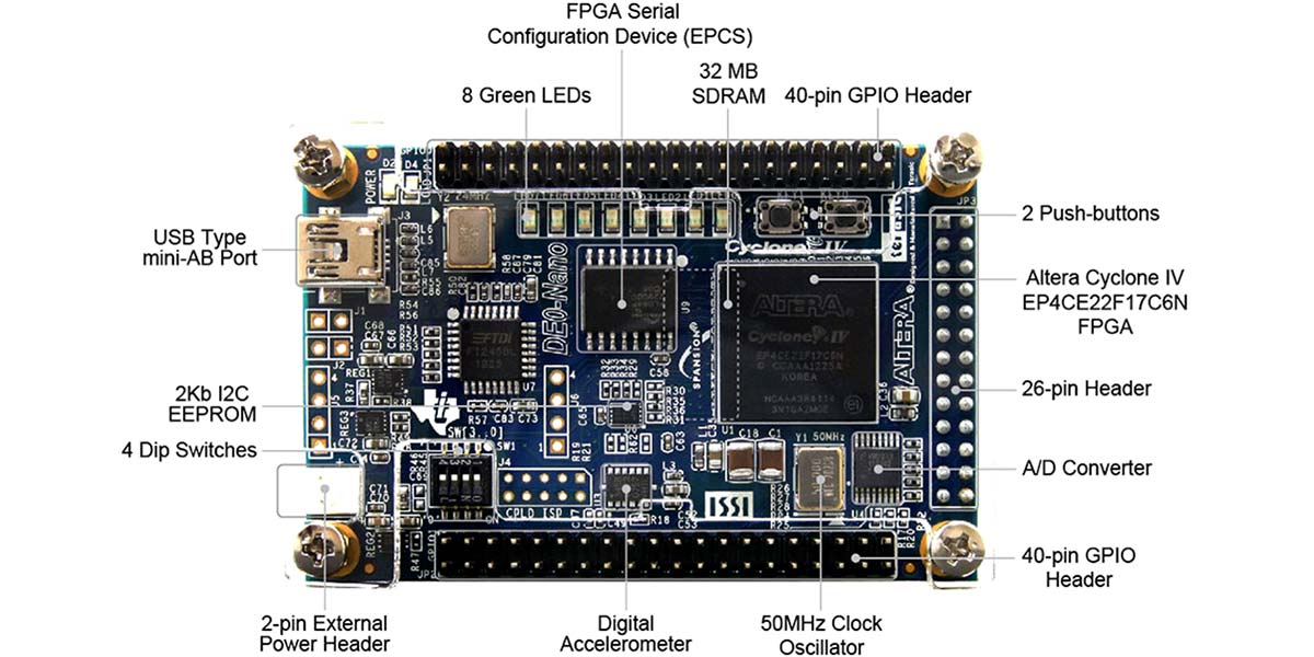
As an example, Terasic (a Taiwanese company) makes a large number of FPGA boards using Altera (Intel) FPGAs. Some — such as the DE0Nano board pictured in Figure 3 — are cheap (~$70) and very easy to use for anyone who wants to learn more about FPGAs. These boards come with detailed documentation on how to use them and exploit their many capabilities.
FIGURE 3. A DE0Nano FPGA development board containing an Intel Cyclone IV FPGA. (Courtesy of Terasic, Inc.)
Along with development boards, one also needs software for writing and compiling HDL code. HDL compilers can be easily downloaded for free from the websites of all FPGA manufacturers. Xilinx offers its ISE and Vivado development suites, while Altera (Intel) makes its Quartus Prime software available (Figure 4) free of charge to all FPGA application developers. These development programs can be used for compiling either VHDL or Verilog code.
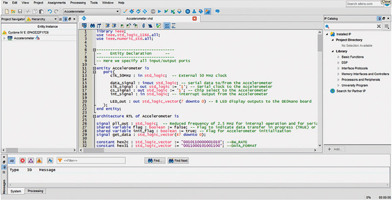
FIGURE 4. Quartus Prime FPGA application development software. (Courtesy of Intel Corporation.)
For a novice, it is best to get hold of any good FPGA development board and begin by writing simple Verilog or VHDL code, compiling it, and downloading it to the FPGA. In most cases, the compiler will flag syntax errors and even logic errors — if any — which is a useful way of learning an HDL.
Once enough practice has been achieved, one can go on to write larger and more useful pieces of code that actually accomplish real functions.
Applying FPGAs
Examples of such applications might include an SD card reader/writer, VGA display controller, real time clock, Ethernet communication module, etc.
It’s possible to use any small development board inside a complete project just as an Arduino board, for example, can be embedded into a project.
Some companies (like Digilent) make small pinned FPGA modules that can be more easily embedded into larger projects as they do not contain extra hardware that full-blown development boards contain. How about including an FPGA chip on your own printed circuit board (PCB)? This can certainly be done, but is somewhat challenging and thus not recommended for beginners.
The majority of FPGA ICs are high (and extremely high) pin count devices, often in hard to solder packages such as ball grid arrays. Their dense pin placement calls for considerable skill on the part of the PCB designer. Added to that is the fact that FPGAs often require multiple supply voltages with many power supply pins that need to be individually bypassed to ground.
FPGA PCB traces are narrow and require extreme care during PCB layout if proper operation has to be guaranteed at high frequencies. For these and other reasons, PCBs hosting FPGAs are considerably hard to design, but can be an interesting challenge for ambitious amateurs.
Final Thoughts
In this introductory two-part series on FPGAs, we have only seen a glimpse of all that is possible with programmable logic devices. There is a lot more to explore out there.
Several books and websites offer help and guidance to FPGA users at all experience levels. Chief among these are FPGA manufacturer’s own websites where one can get an enormous amount of free learning resources targeting all levels of expertise; www.fpga4fun.com is a popular website with several introductory and mid-level projects for hobbyists to build.
A very large number of helpful learner-focussed videos are available on YouTube. As for books, many are available covering FPGAs, VHDL, Verilog, and complete digital system design with programmable logic as a search online will reveal.
After some familiarity has been gained with FPGA configuration concepts through the use of a development board/system software combination, one can graduate to some really interesting projects.
If you have not yet started using FPGAs, then this is the right time to do that. The FPGA ecosystem has matured to such an extent that many interesting devices and development systems (together with abundant support resources) are readily available to ease any beginner’s way through the exciting world of programmable logic. NV