If you are an electronics hobbyist, you often need to generate pulses and logic levels to check out the operation of your circuit before completely finishing the project. If you breadboard a circuit to see if your idea will work, you need signals to check its operation. If your circuit interfaces with the external world, you need to simulate inputs during development. If you experiment with electronics, a pulse generator is a handy tool.
When I started as an electronics hobbyist, my first design was a digital speedometer. I made a pickup that produced a pulse each time the drive shaft made a revolution. I quickly realized that unless my wife drove me up and down the street while I worked on my circuit in the back seat, I needed something to simulate pulses on the workbench. I got through the speedometer project with a 555 timer and a trimpot to simulate the driveline pulses, but my very next project was a general-purpose pulse generator.
This project is an upgraded design that incorporates features I found over the years to be most helpful to an electronics hobbyist. It is an instrument with real knobs that can be quickly and easily adjusted — without soft keys or layered menus.
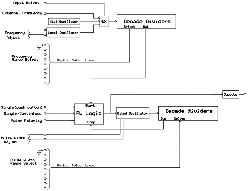
Block Diagram
Experimenter’s Wide Range Pulse Generator
This design is simple and straightforward, using oscillators followed by digital dividers; take a look at the schematic that is shown in Figures 1 and 2. The dividers provide a method of changing the frequency and pulse width ranges with static digital signals instead of capacitor switching, which is the classic method.
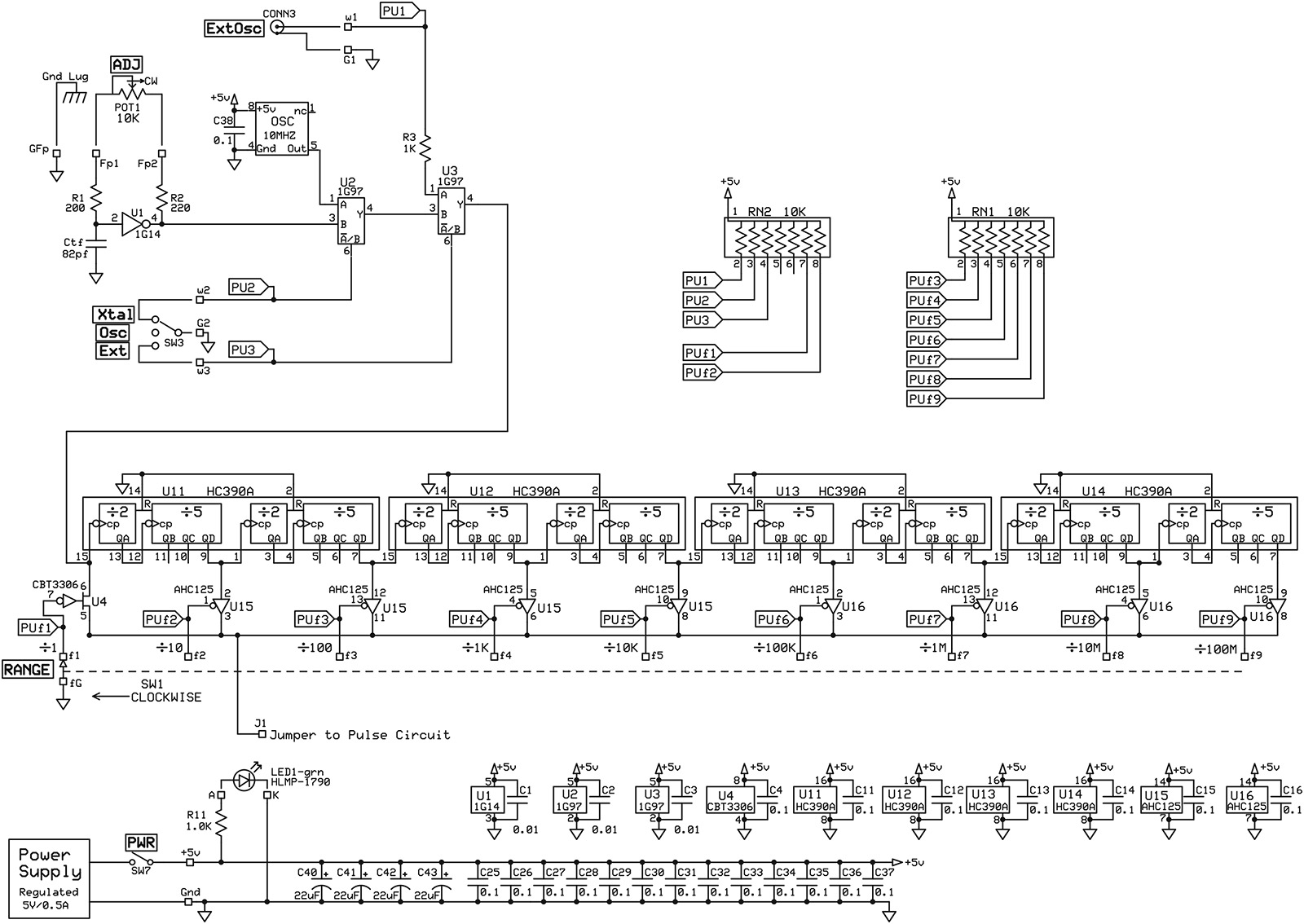
FIGURE 1.
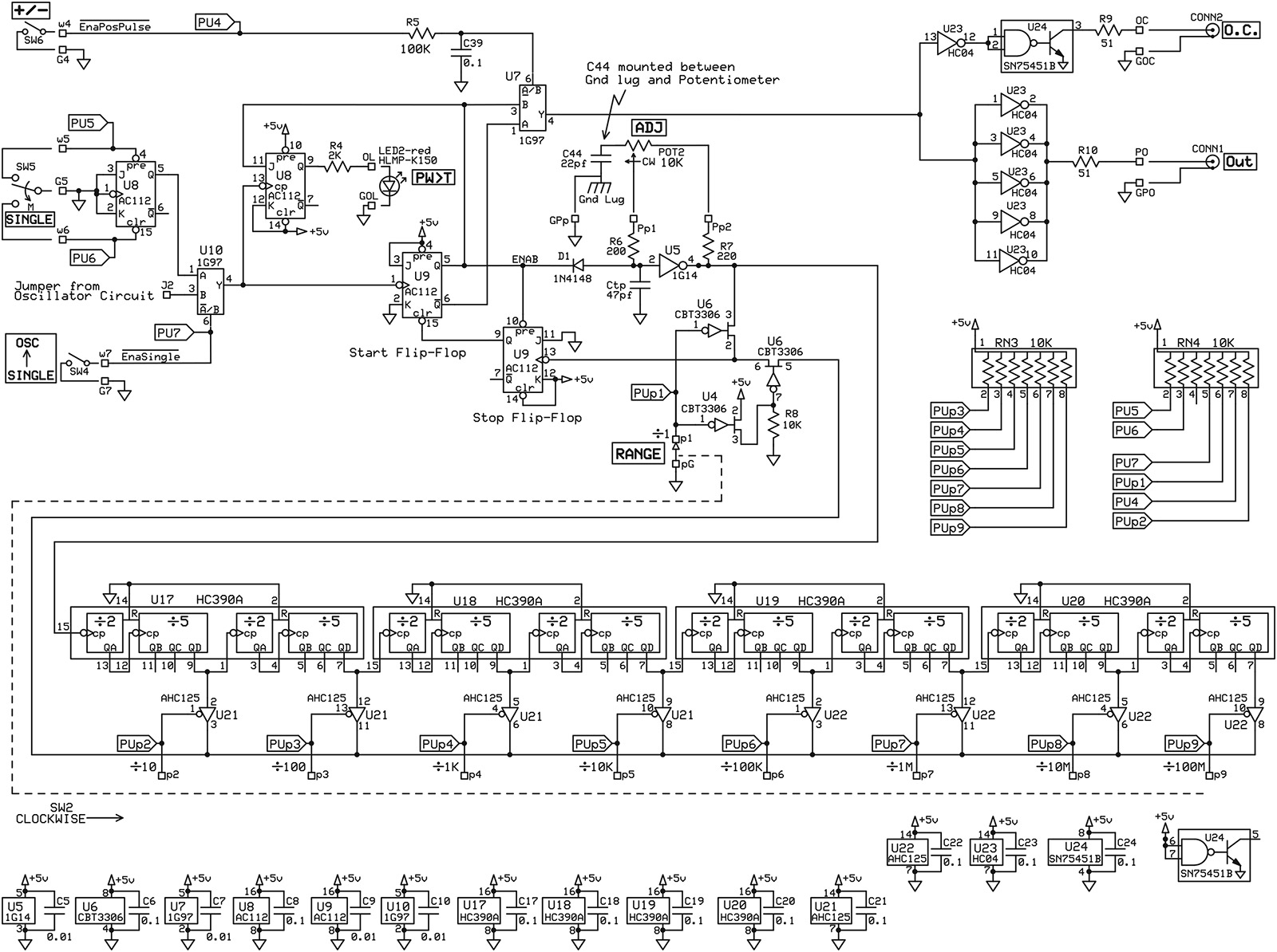
FIGURE 2.
Static digital signals are relatively insensitive to wire length and routing, and eliminate layout headaches as well as tolerance problems that come with the switching of capacitors.
As implemented, the circuit achieves a nine decade range providing frequencies from approximately 20 MHz to 0.01 Hz, and pulse widths from approximately 25 nsec to 100 sec.
The only signals that are sensitive to wire routing are those that adjust the oscillators. The potentiometer leads that go to the Schmitt trigger oscillators must be kept short and neat. Additionally, the circuitry must be enclosed in a metal (conducting/shielding) enclosure to prevent external fields from interfering.
There are two outputs. In addition to a driven 0V to 5V logic level signal output, an open collector output has been implemented. The open collector will require the circuit under test to have a pull-up (to get the high logic level) which will allow the output to match any logic level voltage (e.g., CMOS running at 9V).
An open collector also allows the power supplied to the circuit being tested to be turned off without disconnecting the pulse generator since no current is fed to the test circuit from the open collector output. The open collector is just about the only output I ever use.
To keep things simple, power for the pulse generator is supplied from a regulated 5V wall adapter.
One of the goals of this project was to get an introduction to surface-mount devices (SMD). Some very cool logic functions are only available in SMD packages. The use of SMD parts was minimized to keep soldering on the printed circuit board (PCB) manageable.
To gain experience with different sizes of SMD components, SOIC and SOT packages were chosen. SMD resistors or capacitors were not used because they are very hard to solder, and not necessary to effectively implement the design.
This pulse generator is a complete design and does not need any additional circuits to provide many years of useful service.
It can also be expanded by the experienced hobbyist who might add features such as variable output amplitude or a 50 ohm cable driver.
The Circuit
The frequency and pulse width oscillators are classic Schmitt trigger logic gate oscillators where the capacitor charges and discharges between the thresholds of the Schmitt trigger input. The charge time is adjusted by the external potentiometer.
In the frequency section, the Schmitt trigger oscillator is multiplexed with a crystal oscillator and an external input to allow the user freedom to generate signals as needed for different kinds of troubleshooting. The selected frequency is then applied to the decade divider string.
A specific decade is selected by grounding the corresponding enable line on one of the AHC125 tri-state buffers. Using the crystal oscillator, an accurate frequency every decade from 10.00 MHz to 0.10 Hz can be selected.
The pulse width section is similar but includes a pair of flip-flops (U9) and a diode (D1) to start and stop the oscillator. The pulse width oscillator is stopped when the input to the Schmitt trigger (U5) is held low by grounding the cathode of D1, and is allowed to run when the cathode of diode D1 is held high.
When an edge from the frequency generator clocks the "start" flip-flop high, the oscillator starts. When the selected output of the divider chain clocks the "stop" flip-flop low, the start flip-flop is cleared and the oscillator stops. When the output of the start flip-flop goes back low, the stop flip-flop is preset high, and the circuit is ready for another cycle. The pulse width is the time the oscillator runs before feedback from a selected divider stops it.
In the narrowest pulse range, bus switches (U6) are used to route the oscillator output to the stop flip-flop without propagation delay, and to isolate it from the capacitance of the divider output bus so that narrower pulses can be obtained.
A flip-flop (U8) is used to detect that the pulse width has been set greater than the period of the frequency and may be causing an erratic output. The other half of U8 is used as a switch debouncer for the "single pulse" momentary switch.
The outputs are not intended to be instrument-grade 50 ohm cable drivers. They will, however, do a reasonable job of supplying logic level signals.
Component Selection
The ICs in the oscillator and pulse width start/stop circuits were chosen for high speed. Using other parts may not present a problem, but be aware that substituting any of these may result in lower top end frequencies and wider minimum pulse widths.
Also, the first divider IC (U11 and U17) should be the "A" suffix type specified in order to guarantee operation at the higher frequencies under worst case conditions. Note that the pin numbering on the SOT packages is different for different logic functions.
The potentiometers and rotary switches were selected to be functional at low cost. A true "logarithmic taper" pot would be nice but they are expensive, so an audio pot was chosen. An "audio taper" approximates a log curve with straight lines. The open collector peripheral driver (U24) was chosen for speed, as well as for high current and voltage. It is rated at 30 volts and 300 mA, making it almost indestructible in normal use.
The "pulse out" IC (U23) was chosen for high current drive and speed. The resistor in series with the output is to limit the rise and fall times, and minimize ringing on the output pulse. If you don't need the higher frequencies and the narrower pulse widths, a slower part such as a C04 is worth considering since the slower rise and fall times are less likely to cause some kind of trouble.
The single pulse momentary switch was chosen to be a toggle type so that there would be tactile feedback from the switch when generating a single pulse. Most panel mount pushbutton switches do not have tactile feedback and I find that annoying. (Did it make contact or not?)
Also, pushing in on a switch tends to move an instrument while pushing down on a toggle keeps it in place. Please use any type of momentary switch you like. Acceptable and sometimes superior knobs, switches, pots, etc., can often be found in the surplus market.
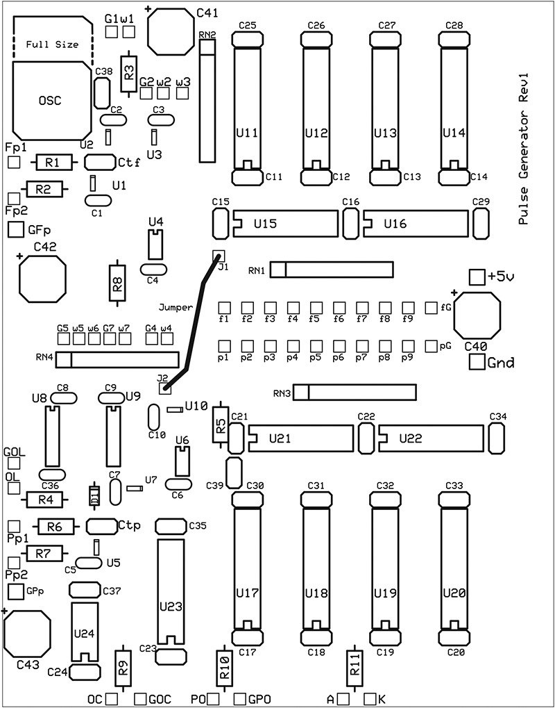
PCB parts placement guide.
Construction
Figures 3 and 4 show the finished project. The enclosure shown is a nice, inexpensive instrument type box from Jameco. It may appear that a much smaller box could be used, but the reduced front panel size would not provide sufficient space for all the knobs and switches. The SMD components were loaded using a fine point soldering iron and tweezers. No special tools were needed. I did find it extremely helpful to get someone else to hold the SMD parts in place until I got one or two leads soldered.
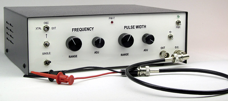
FIGURE 3.
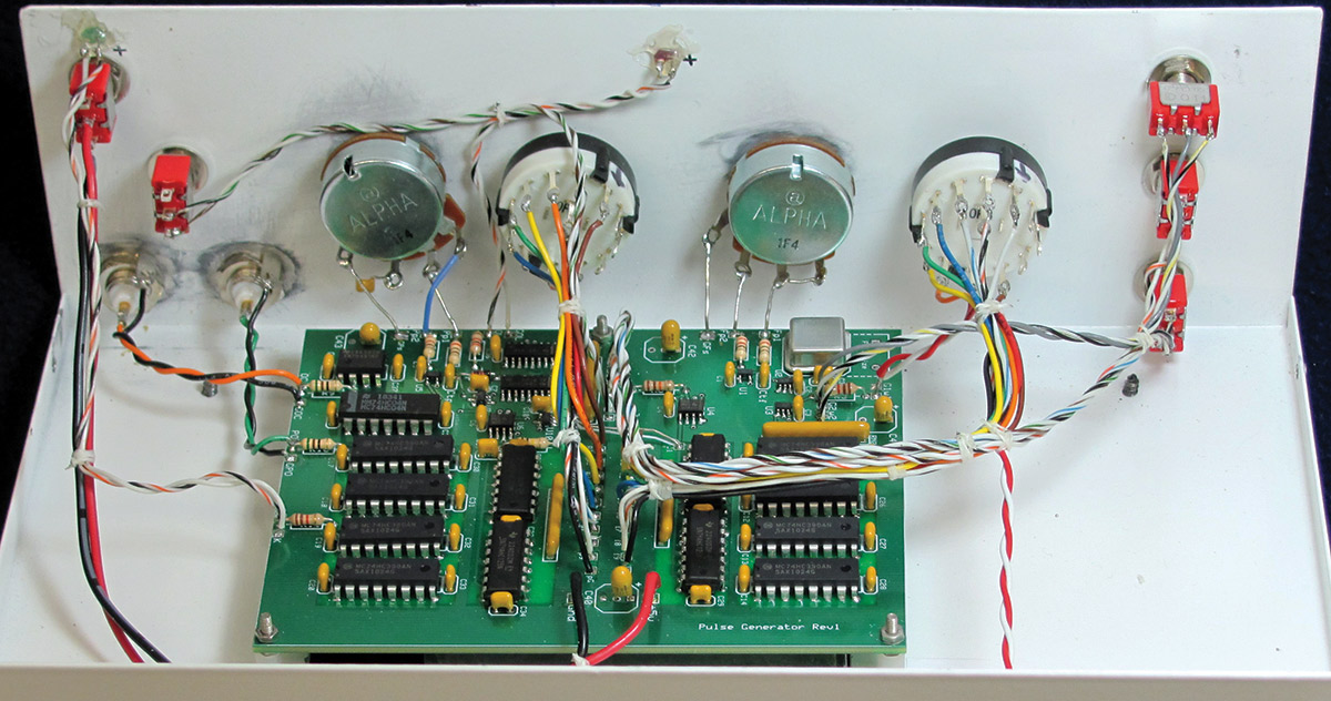
FIGURE 4.
Keep in mind that there is no substitute for careful inspection of SMD soldering. (I recommend you read the article How To: Surface Mount Soldering, by R.L. Doerr.) There are some good DIY videos on the Internet. Be careful to orient the ICs correctly.
The parts are mounted in varying directions on the PCB to keep the traces short — especially in the high frequency area. I suggest you load the SMD components first to give the best access to the very small pins you will be soldering. You may want to use a larger soldering iron tip on the thru-hole parts as the power planes are heatsinking.
One of the more difficult parts of any homemade equipment is creating a good looking front panel. I chose a minimalist approach, i.e., just enough lettering to identify the various controls and switches, and no more.
The front panel is drilled before the lettering is applied, eliminating a lot of planning and coordination of the exact location of the switches and potentiometers. That is, the holes for the switches do not have to be placed in precise locations to match the lettering; the lettering is placed after the holes are drilled.
Using self-adhesive paper (Avery labels), I print the lettering with an inkjet printer and then seal the print with a spray-on fixative. The lettering is then cut to size and applied to the front panel. This technique creates a functional and good looking front panel with minimal effort. (Or, you can use services from companies such as FrontPanelExpress.com.) Feel free to rearrange the front panel to suit your needs.
Any single pole rotary switch with nine or more positions can be used. A common variety found in the hobby/surplus market is the one pole/12 position type. The specified switch (Mammoth Electronics #820-1P2-12T) has a stop feature that allows rotation to be limited to the nine positions needed for this project.
If you choose to use a switch without a "position stop," connect the extra positions together with the first or last position so the circuit outputs a signal when one of the extra positions is selected.
Note: When wiring the frequency range switch (SW1), increasing frequency with clockwise rotation requires the switch to be wired in the opposite direction of the schematic numbering: f1 goes to switch position 9; f2 goes to switch position 8; etc.
The potentiometer housings need to be grounded to stabilize stray capacitance in the oscillator adjustment circuits. Start by scraping the paint on the inside of the front panel around the potentiometer's mounting hole. Then, use a grounding lug with a star washer when mounting the pot. Connect the lug to ground using the corresponding hole provided on the PCB (GFp and GPp). If you don't have a grounding lug, you can wrap a piece of bus wire around the bushing and use a regular star washer.
Note: Capacitor C44 is mounted at the pulse width ADJ potentiometer (POT2) between the potentiometer and the ground lug (wire); see Figure 5.
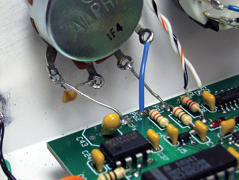
FIGURE 5.
A grounding lug is specified in the Parts List. Wiring to the switches is not critical. Just hook them up neatly and you will be fine. (Refer back to Figure 4.) The LEDs are held in place with glue.
| QTY |
DESIGNATOR |
DESCRIPTION |
| 7 |
C1-C3, C5, C7, C9, C10 |
0.01, radial ceramic, 50V, 10%, XR7 |
| 32 |
C4, C6, C8, C11-C39 |
0.1, radial ceramic, 50V, 20%, Z5U |
| 4 |
C40-C43 |
22 µF, 10V |
| 1 |
C44 |
22 pF, radial ceramic, 100V, 5%, C0G (NP0) |
| 1 |
Ctf |
82 pF, radial ceramic, 100V, 5%, C0G (NP0) |
| 1 |
Ctp |
47 pF, radial ceramic, 100V, 5%, C0G (NP0) |
| 1 |
D1 |
1N4148 |
| 1 |
OSC |
10 MHz |
| 1 |
R1 |
200, 5%, 1/4 watt |
| 1 |
R2 |
220, 5%, 1/4 watt |
| 3 |
R3, R4, R11 |
1K, 5%, 1/4 watt |
| 1 |
R5 |
100K, 5%, 1/4 watt |
| 1 |
R6 |
200, 5%, 1/4 watt |
| 1 |
R7 |
220, 5%, 1/4 watt |
| 1 |
R8 |
10K, 5%, 1/4 watt |
| 2 |
R9, R10 |
51, 5%, 1/4 watt |
| 4 |
RN1-RN4 |
10K Eight-pin resistor network-bussed |
| 2 |
U1, U5 |
Schmitt trigger inverter - SOT-23 |
| 4 |
U2, U3, U7, U10 |
Configurable multi-function gate - SOT-23 |
| 2 |
U4, U6 |
Dual FET bus switch - SOIC |
| 2 |
U8, U9 |
Dual J-K flip-flop - SOIC |
| 8 |
U11-U15, U17-U20 |
Dual decade counters - DIP |
| 4 |
U15, U16, U21,U22 |
Quad bus buffer gate - DIP |
| 1 |
U23 |
Hex inverter - DIP |
| 1 |
U24 |
Dual peripheral drivers - DIP |
| PANEL MOUNT COMPONENTS |
| 1 |
LED1 |
Green |
| 1 |
LED2 |
Red |
| 2 |
POT1, POT2 |
10K audio |
| 2 |
SW1, SW2 |
Rotary switch, SP-12 pos |
| 1 |
SW3 |
Toggle switch, SPDT on-none-on |
| 1 |
SW4 |
Momentary toggle switch, SPDT on-(on) |
| 3 |
SW5-SW7 |
Toggle switch, SPDT on-on |
| 3 |
|
BNC or RCA phono jacks |
| 2 |
|
Grounding lugs |
| 2 |
|
Knob/range |
| 2 |
|
Knob/adj |
| 1 |
|
Instrument case |
| 1 |
|
Power supply, 5V/0.5A regulated |
| A more detailed Parts List with both manufacturer and distributor part numbers is available in the downloads. |
PARTS LIST.
Either RCA phono jacks or BNC connectors can be used for the outputs. The phono jacks are much less expensive, and sufficient for most uses. Wiring to the outputs should be short and neat twisted pairs.
The outer ring of the connectors should also be connected to the case by removing the paint and using a star washer.
When mounting the PCB, use metal stand-offs and star washers so that the ground plane (top side) is connected to the case. The external input was placed on the rear panel, assuming infrequent use.
If you don't implement the complete circuit, be sure to pull up or pull down any unused inputs (e.g., if the crystal oscillator is not loaded, a 10K resistor from the crystal oscillator output on the PCB to either +5V or Gnd will keep U2 pin 1 from floating).
After the PCB is loaded, temporarily wire in the ADJ pots and verify the functionality of the circuit (just in case there is a solder bridge or other problem). Using temporary connections (clip leads/wires), check all switch functions.
Using the Pulse Generator
The pulse generator is used to create logic level signals that are needed to check out electronic projects. It can be used during the design, development, or checkout of logic or microprocessor circuits where external inputs need to be simulated.
I have recently used it on projects such as an anemometer, an automobile over-speed alarm, and a stepper motor controller.
The pulse generator typically provides pulses simulating a "logic clock" but can also be used in less obvious ways. For example, a 1 Hz frequency can easily and accurately be obtained by setting the frequency to 1.000 kHz and then changing the "range" switch by three decades to get to an output of 1 Hz.
Another use that may not be obvious is to put the generator in the "single" mode and flip the polarity switch (±); you now have a logic level that can be changed without the "contact bouncing" that occurs when connecting and disconnecting a clip lead.
Please try using the open collector output. This approach can save hours of confusion that is caused when inadvertently powering a circuit from the driven output of a signal source, or breaking something by driving current into it unintentionally.
The PCB is available at the Nuts & Volts webstore. If you wish to have your own boards made, I have included the Express PCB board files and additional drawings and information in the downloads. NV
