Practical applications of MOSFETs and CMOS-based MOSFET devices.
Part 1 of this series explained (among other things) the basic operating principles of the MOSFET (or IGFET), and pointed out that complementary enhancement-mode pairs of these devices form the basis of the digital technology known as CMOS.
The present episode of the series looks at practical applications of MOSFETs and CMOS-based MOSFET devices.
A MOSFET INTRODUCTION
MOSFETs are available in both depletion-mode and enhancement-mode versions. Depletion-mode types give a performance similar to a JFET, but with a far higher input resistance (i.e., with a far higher low-frequency input impedance).
 |
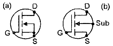 |
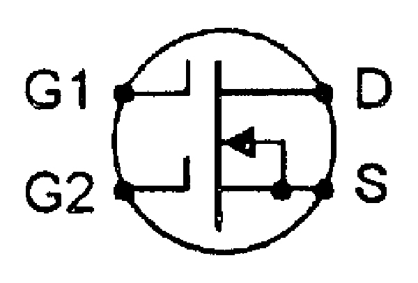
FIGURE 1. Symbol of the dual-gate or tetrode
MOSFET. |
FIGURE 2. Standard symbols of (a) three-pin and (b) four-pin
n-channel enhancement-mode MOSFETs. |
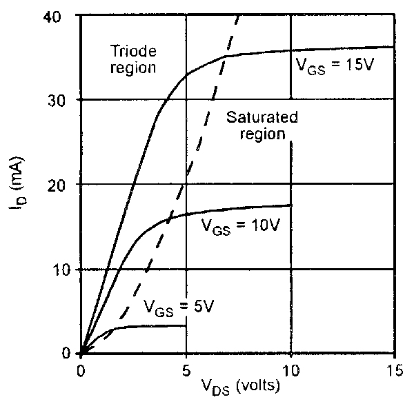 |
| FIGURE 3. Typical transfer characteristics of 4007UB n-channel enhancement-mode MOSFETs. |
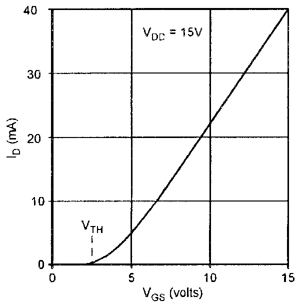 |
| FIGURE 4. Typical VGS/ID characteristics of 4007UB n-channel enhancement-mode MOSFET. |
Some depletion-mode MOSFETs are equipped with two independent gates, enabling the drain-to-source currents to be controlled via either one or both of the gates; these devices (which are often used as signal mixers in VHF tuners) are known as dual-gate or tetrode MOSFETs, and use the symbol shown in Figure 1.
Most modern MOSFETs are enhancement-mode devices, in which the drain-to-source conduction channel is closed when the gate bias is zero, but can be opened by applying a forward gate bias. This ‘normally open-circuit’ action is implied by the gaps between source and drain in the device’s standard symbol, shown in Figure 2(a), which depicts an n-channel MOSFET (the arrow head is reversed in a p-channel device). In some devices, the semiconductor substrate is made externally available, creating a ‘four-terminal’ MOSFET, as shown in Figure 2(b).
Figure 3 shows typical transfer characteristics of an n-channel enhancement-mode MOSFET, and Figure 4 shows the VGS/ID curves of the same device when powered from a 15V supply. Note that no significant ID current flows until the gate voltage rises to a threshold (VTH) value of a few volts but that, beyond this value, the drain current rises in a non-linear fashion.
Also note that the Figure 3 graph is divided into two characteristic regions, as indicated by the dotted line; these being the ‘triode’ region, in which the MOSFET acts like a voltage-controlled resistor, and the ‘saturated’ region,’ in which it acts like a voltage-controlled constant-current generator.
Because of their very high input resistances, MOSFETs are vulnerable to damage via electrostatic discharges; for this reason, MOSFETs are sometimes provided with integral protection via diodes or zeners.
THE 4007UB
The easiest and cheapest practical way of learning about enhancement-mode MOSFETs is via a 4007UB IC, which is the simplest member of the popular CMOS ‘4000-series’ digital IC range, and actually houses six useful MOSFETs in a single 14-pin DIL package.
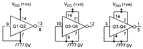
Figure 5 shows the functional diagram and pin numbers of the 4007UB, which houses two complementary pairs of independently-accessible MOSFETs and a third complementary MOSFET pair that is connected as a standard CMOS inverter stage.
 |
 |
| FIGURE 5. Functional diagram of the 4007UB dual CMOS pair plus inverter. |
FIGURE 6. Internal protection network (within dotted lines) on each input of the 4007UB. |
Each of the IC’s three independent input terminals is internally connected to the standard CMOS protection network shown in Figure 6.
Within the IC, Q1, Q3, and Q5 are p-channel MOSFETs, and Q2, Q4, and Q6 are n-channel types. Note that the performance graphs of Figures 3 and 4 actually apply to the individual n-channel devices within this CMOS IC.
 |
| FIGURE 7. Individual 4007UB complementary pairs can be disabled by connecting them as CMOS inverters and grounding their inputs. |
The 4007UB usage rules are simple. In any given application, all unused IC elements must be disabled. Complementary pairs of MOSFETs can be disabled by connecting them as standard CMOS inverters (i.e., gate-to-gate and source-to-source) and tying their inputs to ground, as shown in Figure 7.
Individual MOSFETs can be disabled by tying their source to their substrate and leaving the drain open circuit. In use, the IC’s input terminal must not be allowed to rise above VDD (the supply voltage) or fall below VSS (zero volts).
To use an n-channel MOSFET, the source must be tied to VSS, either directly or via a current-limiting resistor. To use a p-channel MOSFET, the source must be tied to VDD, either directly or via a current-limiting resistor.
LINEAR OPERATION
To fully understand the operation and vagaries of CMOS circuitry, it is necessary to understand the linear characteristics of basic MOSFETs, as shown in the graph of Figure 4.
Note that negligible drain current flows until the gate rises to a ‘threshold’ value of about 1.5 to 2.5 volts, but that the drain current then increases almost linearly with further increases in gate voltage.
Figure 8 shows how to use an n-channel 4007UB MOSFET as a linear inverting amplifier. R1 acts as Q2’s drain load, and R2-Rx bias the gate so that Q2 operates in the linear mode.
The Rx value is selected to give the desired quiescent drain voltage, and is normally in the 18k to 100k range.
 |
 |
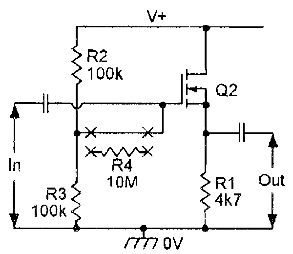 |
Figure 8. Method of biasing n-channel 4007UB MOSFETs for use as a linear inverting
amplifier (with medium input impedance). |
Figure 9. High impedance version of the inverting amplifier. |
Figure 10. Methods of biasing n-channel 4007UB MOSFET as a unity-gain non-inverting amplifier or source follower. |
The amplifier can be made to give a very high input impedance by wiring a 10M isolating resistor between the R2-Rx junction and Q2 gate, as shown in Figure 9.Figure 10 shows how to use an n-channel MOSFET as a unity-gain non-inverting common-drain amplifier or source follower.
The MOSFET gate is biased at half-supply volts by the R2-R3 divider, and the source terminal automatically takes up a quiescent value that is slightly more than VTH below the gate value.
The basic circuit has an input impedance equal to the paralleled values of R2 and R3 (=50k), but can be increased to greater than 10M by wiring R4 as shown.
 |
| FIGURE 11. Bootstrapped source follower has ultra-high input impedance. |
Alternatively, the input impedance can be raised to several hundred megohms by bootstrapping R4 via C1 as shown in Figure 11.
Note from the above description that the enhancement-mode MOSFET performs like a conventional bipolar transistor, except that it has an ultra-high input impedance and has a substantially larger input-offset voltage (the base-to-emitter offset of a bipolar is typically 600mV, while the gate-to-source offset voltage of a MOSFET is typically two volts).
Allowing for these differences, the enhancement-mode MOSFET can thus be used as a direct replacement in many small-signal bipolar transistor circuits.
THE CMOS INVERTER
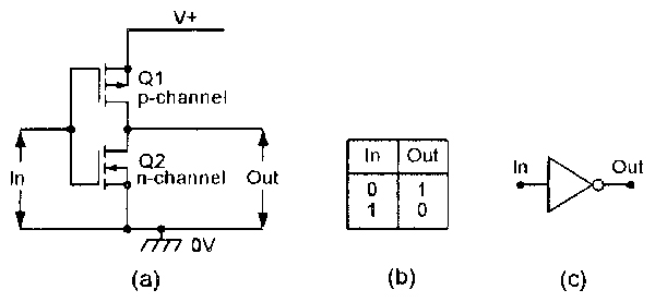
A major application of enhancement-mode MOSFETs is in the basic CMOS inverting stage of Figure 12(a), in which an n-channel and a p-channel pair of MOSFETs are wired in series but share common input and output terminals.
This basic CMOS circuit is primarily meant for use in digital applications (as described towards the end of Part 1 of this series), in which it consumes negligible quiescent current but can source or sink substantial output currents.
 |
| FIGURE 12. Circuit (a), truth table (b), and symbol (c) of the basic CMOS digital inverter. |
Figures 12(b) and 12(c) show the inverter’s digital truth table and its circuit symbol. Note that Q5 and Q6 of the 4007UB IC are fixed-wired in the CMOS inverter configuration.
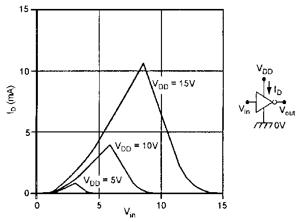
Although intended primarily for digital use, the basic CMOS inverter can be used as a linear amplifier by biasing its input to a value between the logic-0 and logic-1 levels; under this condition Q1 and Q2 are both biased partly on, and the inverter thus passes significant quiescent current.
Figure 13 shows the typical drain-current (ID) transfer characteristics of the circuit under this condition; ID is zero when the input is at zero or full supply volts, but rises to a maximum value (typically 0.5mA at 5V, or 10.5mA at 15V) when the input is at roughly half-supply volts, under which condition both MOSFETs of the inverter are biased equally.
 |
 |
| FIGURE 13. Drain-current transfer characteristics of the simple CMOS inverter. |
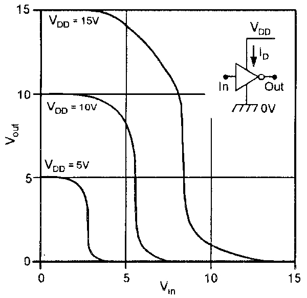
FIGURE 14. Typical input-to-output
voltage transfer characteristics of the 4007UB simple CMOS inverter. |
 |
| FIGURE 15. Method of biasing the simple CMOS inverter for linear operation. |
Figure 14 shows the typical input-to-output voltage-transfer characteristics of the simple CMOS inverter at different supply voltage values. Note that the output voltage changes by only a small amount when the input voltage is shifted around the VDD and 0V levels, but that when Vin is biased at roughly half-supply volts, a small change of input voltage causes a large change of output voltage.
Typically, the inverter gives a voltage gain of about 30dB when used with a 15V supply, or 40dB at 5V.
Figure 15 shows a practical linear CMOS inverting amplifier stage. It is biased by wiring 10M resistor R1 between the input and output terminals, so that the output self-biases at approximately half-supply volts.
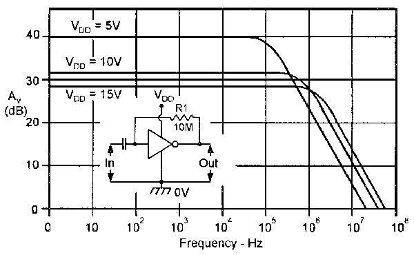 |
FIGURE 16. Typical AV and frequency characteristics
of the linear-mode basic CMOS amplifier. |
Figure 16 shows the typical voltage gain and frequency characteristics of this circuit when operated at three alternative supply rail values; this graph assumes that the amplifier output is feeding into the high impedance of a 10M/15pF oscilloscope probe and, under this condition, the circuit has a bandwidth of 2.5MHz when operating from a 15V supply.
As would be expected from the voltage transfer graph of Figure 14, the distortion characteristics of the CMOS linear amplifier are quite good with small-amplitude signals (output amplitudes up to 3V peak-to-peak with a 15V supply), but the distortion then increases as the output approaches the upper and lower supply limits. Unlike a bipolar transistor circuit, the CMOS amplifier does not ‘clip’ excessive sinewave signals, but progressively rounds off their peaks.
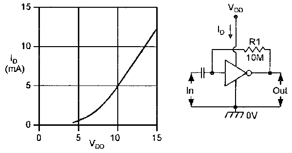 |
Figure 17. Typical ID/VDD characteristics of the
linear-mode CMOS amplifier. |
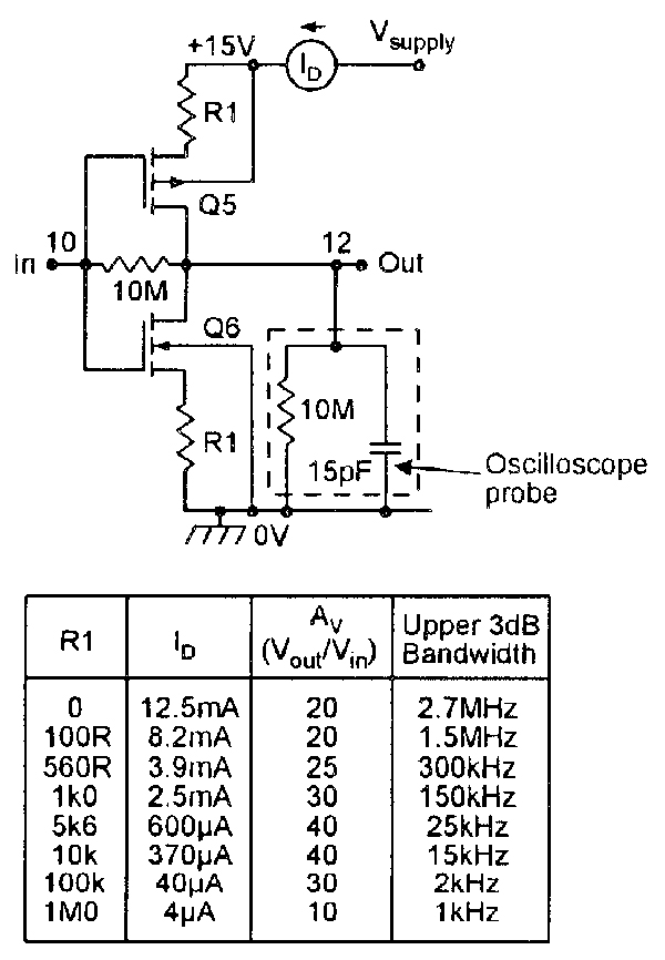 |
FIGURE 18. Micropower 4007UB CMOS linear amplifier, showing method of reducing ID, with
performance details. |
Figure 17 shows the typical drain-current versus supply-voltage characteristics of the CMOS linear amplifier. The current typically varies from 0.5mA at 5V, to 12.5mA at 15V.
In many applications, the quiescent supply current of the 4007UB CMOS amplifier can be usefully reduced — at the cost of reduced amplifier bandwidth — by wiring external resistors in series with the source terminals of the two MOSFETs of the CMOS stage, as shown in the ‘micropower’ circuit of Figure 18.
This diagram also lists the effects that different resistor values have on the drain current, voltage gain, and bandwidth of the amplifier when operated from a 15V supply and with its output loaded by a 10M/15pF oscilloscope probe.
Note that the additional resistors of the Figure 18 circuit increase the output impedance of the amplifier (the output impedance is roughly equal to the R1-AV product), and this impedance and the external load resistance/capacitance has a great effect on the overall gain and bandwidth of the circuit.
When using a 10k value for R1, for example, if the load capacitance is increased (from 15pF) to 50pF, the bandwidth falls to about 4kHz, but if the capacitance is reduced to 5pF, the bandwidth increases to 45kHz. Similarly, if the resistive load is reduced from 10M to 10k, the voltage gain falls to unity; for significant gain, the load resistance must be large relative to the output impedance of the amplifier.
The basic (unbiased) CMOS inverter stage has an input capacitance of about 5pF and an input resistance of near-infinity. Thus, if the output of the Figure 18 circuit is fed directly to such a load, it shows a voltage gain of x30 and a bandwidth of 3kHz when R1 has a value of 1M0; it even gives a useful gain and bandwidth when R1 has a value of 10M, but consumes a quiescent current of only 0.4µA.
PRACTICAL CMOS
The CMOS linear amplifier can easily be used in either its standard or micropower forms to make a variety of fixed-gain amplifiers, mixers, integrators, active filters, and oscillators, etc. A selection of such circuits is shown in Figures 19 to 23.
 |
 |
 |
 |
| FIGURE 19. Linear CMOS amplifier wired as x10 inverting amplifier. |
FIGURE 20. Linear CMOS amplifier wired as unity-gain four-input audio mixer. |
FIGURE 21. Linear CMOS amplifier wired as an integrator. |
FIGURE 22. Linear CMOS
amplifier wired as a
crystal oscillator. |
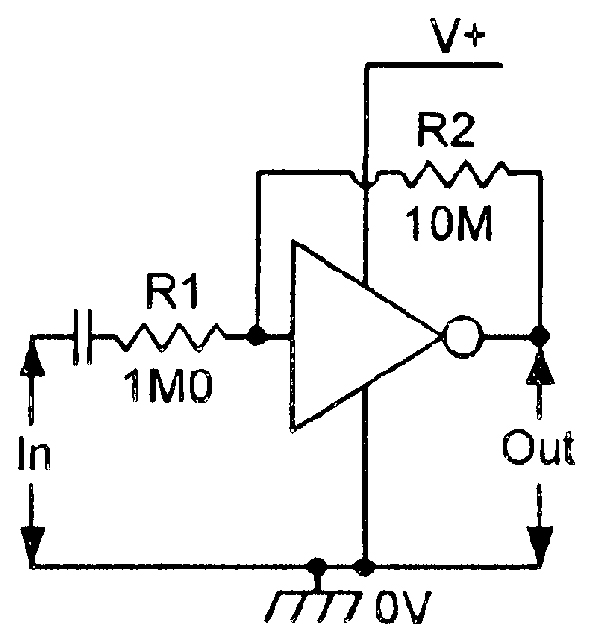
Figure 19 shows the practical circuit of an x10 inverting amplifier. The CMOS stage is biased by feedback resistor R2, and the voltage gain is set at x10 by the R1/R2 ratio. The input impedance of the circuit is 1M0, and equals the R1 value.
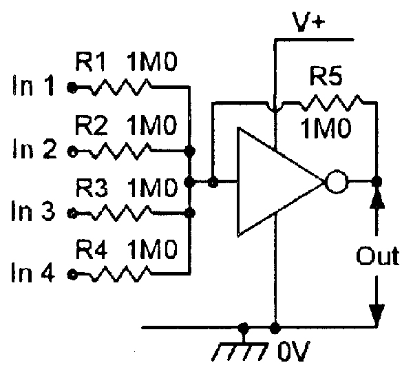
Figure 20 shows the above circuit modified for use as an audio ‘mixer’ or analog voltage adder. The circuit has four input terminals, and the voltage gain between each input and the output is fixed at unity by the relative values of the 1M0 input resistor and the 1M0 feedback resistor.
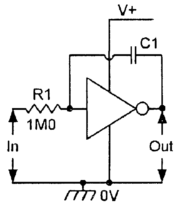
Figure 21 shows the basic CMOS amplifier used as a simple integrator.
 |
| FIGURE 23. Micropower version of the crystal oscillator. |
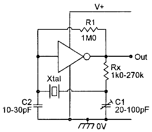
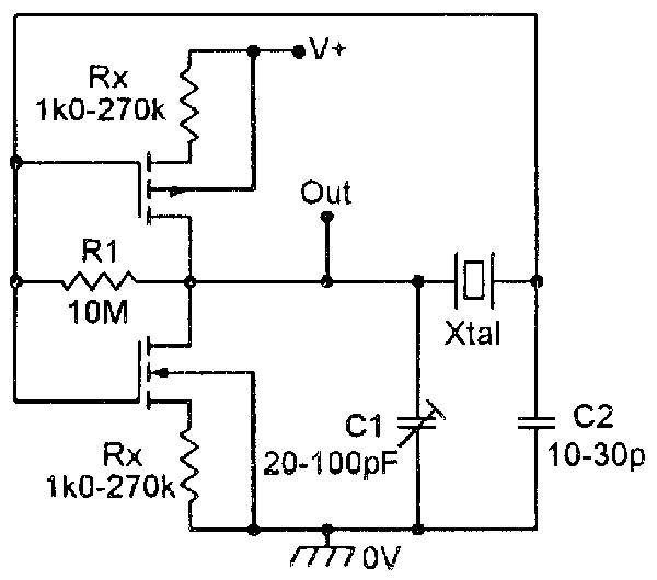
Figure 22 shows the linear CMOS amplifier used as a crystal oscillator. The amplifier is linearly biased via R1 and provides 180° of phase shift at the crystal resonant frequency, thus enabling the circuit to oscillate. If the user wants the crystal to provide a frequency accuracy within 0.1% or so, Rx can be replaced by a short and C1-C2 can be omitted. For ultra-high accuracy, the correct values of Rx-C1-C2 must be individually determined (the diagram shows the typical range of values).
Finally, Figure 23 shows a ‘micropower’ version of the CMOS crystal oscillator. In this case, Rx is actually incorporated in the amplifier. If desired, the output of this oscillator can be fed directly to the input of an additional CMOS inverter stage, for improved waveform shape/amplitude. NV
Other Parts In the FET Principles And Circuits Series — Coming Weekly
FET (Field-Effect Transistor) basics. (Part 1 of 4)
Practical JFET circuits. (Part 2 of 4)
Practical MOSFET and CMOS circuits. (Part 3 of 4)