Practical VMOS power FET circuits and applications.
Part 1 of this series explained (among other things) the basic operating principles of those enhancement-mode power-FET devices known as VFETs or VMOS. This final episode of the series takes a deeper look at these devices and shows practical ways of using them.
A VMOS INTRODUCTION
A VFET can, for most practical purposes, be simply regarded as a high-power version of a conventional enhancement-mode MOSFET. The specific form of VFET construction shown in Figure 17 in Part 1 of this series was pioneered by Siliconix in the mid-1970s, and the devices using this construction are marketed under the trade name ‘VMOS power FETs’ (Vertically-structured Metal-Oxide Silicon power Field-Effect Transistors). This ‘VMOS’ name is traditionally associated with the V-shaped groove formed in the structure of the original (1976) versions of the device.
 |
 |
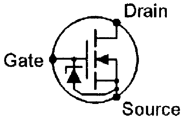
| FIGURE 1. Symbol of Siliconix VMOS power FET with integral zener diode gate protection. |
FIGURE 2.
Major parameters of five popular n-channel Siliconix VMOS power FETs. |
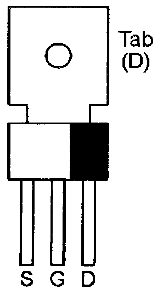 |
FIGURE 3. Outline
and pin connections
of the TO202-cased VN66AF power FET. |
Siliconix VMOS power FETs are probably the best known type of VFETs. They are available as n-channel devices only, and usually incorporate an integral zener diode which gives the gate a high degree of protection against accidental damage; Figure 1 shows the standard symbol used to represent such a device, and Figure 2 lists the main characteristics of five of the most popular members of the VMOS family; note in particular the very high maximum operating frequencies of these devices.
Other well-known families of ‘Vertically-structured’ power MOSFETS are those produced by Hitachi, Supertex, and Farranti, etc. Some of these V-type power MOSFETs are available in both n-channel and p-channel versions and are useful in various high-performance complementary audio power amplifier applications.
THE VN66AF
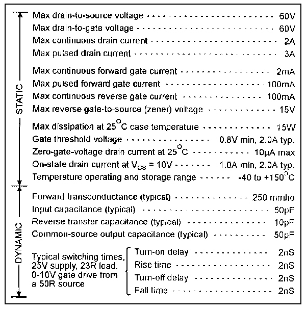 |
| FIGURE 4. Major static and dynamic characteristics of the VN66AF. |
The best way to get to know VMOS is to actually ‘play’ with it, and the readily available Siliconix VN66AF is ideal for this purpose. It is normally housed in a TO202-style plastic-with-metal-tab package with the outline and pin connections shown in Figure 3.
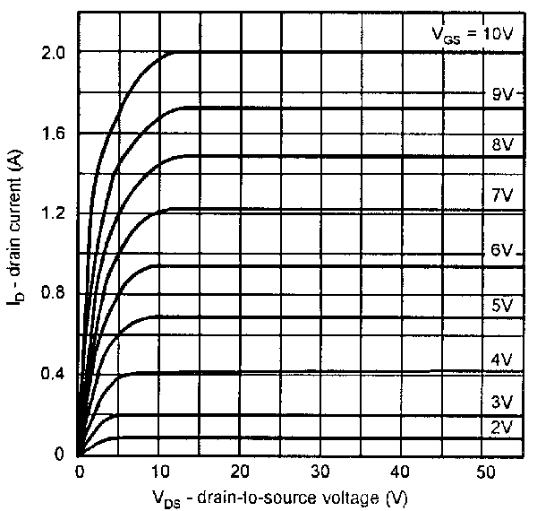
Figure 4 lists the major static and dynamic characteristics of the VN66AF. Points to note here are that the input (gate-to-source) signal must not exceed the unit’s 15V zener rating, and that the device has a typical dynamic input capacitance of 50pF. This capacitance dictates the dynamic input impedance of the VN66AF; the static input impedance is of the order of a million megohms. Figures 5 and 6 show the VN66AF’s typical output and saturation characteristics. Note the following specific points from these graphs.
- The device passes negligible drain current until the gate voltage reaches a threshold value of about 1V; the drain current then increases non-linearity as the gate is varied up to about 4V, at which point the drain current value is about 400mA; the device has a square-law transfer characteristic below 400mA.
- The device has a highly linear transfer characteristic above 400mA (4V on the gate) and thus offers good results as a low-distortion class-A power amplifier.
- The drain current is controlled almost entirely by the gate voltage and is almost independent of the drain voltage so long as the device is not saturated. A point not shown in the diagram is that, for a given value of gate voltage, the drain current has a negative temperature coefficient of about 0.7% per °C, so that the drain current decreases as temperature rises. This characteristic gives a fair degree of protection against thermal runaway.
- When the device is saturated (switched fully on) the drain-to-source path acts as an almost pure resistance with a value controlled by the gate voltage. The resistance is typically 2R0 when 10V is on the gate, and 10R when 2V is on the gate. The device’s ‘off’ resistance is in the order of megohms. These features make the device highly suitable for use as a low-distortion high-speed analog power switch.
 |
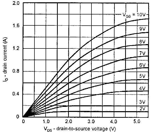 |
| FIGURE 5. Typical output characteristics of the VN66AF. |
FIGURE 6. Typical saturation characteristics of the VN66AF. |
DIGITAL CIRCUITS
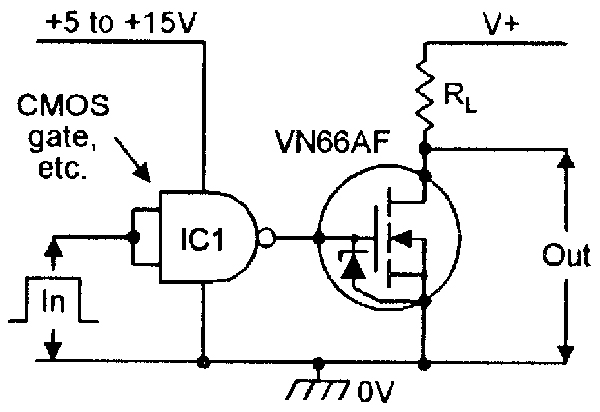
VMOS can be used in a wide variety of digital and analog applications. It is delightfully easy to use in digital switching and amplifying applications; Figure 7 shows the basic connections. The load is wired between the drain and the positive supply rail, and the digital input signal is fed directly to the gate terminal. Switch-off occurs when the input goes below the gate threshold value (typically about 1.2V). The drain ON current is determined by the peak amplitude of the gate signal, as shown in Figure 5, unless saturation occurs. In most digital applications, the ON current should be chosen to ensure saturation.
The static input impedance of VMOS is virtually infinite, so zero drive power is needed to maintain the VN66AF in the ON or OFF state. Drive power is, however, needed to switch the device from one state to the other; this power is absorbed in charging or discharging the 50pF input capacitance of the VN66AF.
The rise and fall times of the output of the Figure 7 circuit are (assuming zero input rise and fall times) determined by the source impedance of the input signal, by the input capacitance and forward transconductance of the VMOS device, and by the value of RL. If RL is large compared to RS, the VN66AF gives rise and fall times of roughly 0.11nS per ohm of RS value. Thus, a 100R source impedance gives a 11nS rise or fall time. If RL is not large compared to RS, these times may be considerably changed.
 |
 |
 |
| FIGURE 7. Basic VMOS digital switch or amplifier. |
FIGURE 8. Methods of driving VMOS from CMOS. |
FIGURE 9. Method of driving VMOS from TTL. |
A point to note when driving the VN66AF in digital applications is that its zener forward and reverse ratings must never be exceeded. Also, because of the very high frequency response of VMOS, the device is prone to unwanted oscillations if its circuitry is poorly designed. Gate leads should be kept short, or be protected with a ferrite bead or a small resistor in series with the gate.
VMOS can be interfaced directly to the output of a CMOS IC, as shown in Figure 8. Output rise and fall times of about 60nS can be expected, due to the limited output currents available from a single CMOS gate, etc. Rise and fall times can be reduced by driving the VMOS from a number of CMOS gates wired in parallel, or by using a special high-current driver.
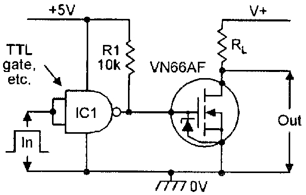
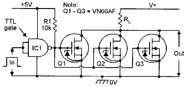
VMOS can be interfaced to the output of TTL by using a pull-up resistor on the TTL output, as shown in Figure 9. The 5V TTL output of this circuit is sufficient to drive 600mA through a single VN66AF. Higher output currents can be obtained either by wiring a level-shifter stage between the TTL output and the VMOS input, or by wiring a number of VMOS devices in parallel, as shown in Figure 10.
 |
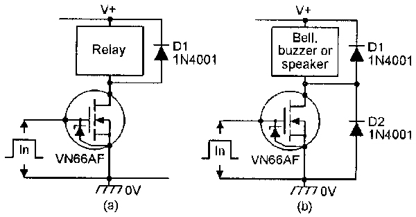 |
FIGURE 10. Method of boosting the output of
Figure 9 by driving three VN66AFs inparallel. |
FIGURE 11. If inductive loads such as relays (a) or bells, buzzers, or speakers (b) are used in digital switchingcircuits, protection diodes must
be wired as shown. |
When using VMOS in digital switching applications, note that if inductive drain loads such as relays, self-interrupting bells or buzzers, or moving-coil speakers are used, clamping diodes must be connected as shown in Figure 11, to damp inductive back-EMFs and thus protect the VMOS device against damage.
SOME DIGITAL DESIGNS
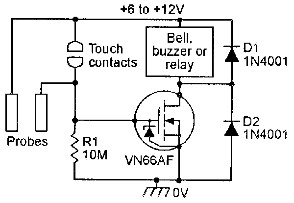
Figures 12 to 15 show a few simple but useful digital applications of the VN66AF. The water- or touch-activated power switch of Figure 12 could not be simpler: when the touch contacts and water probes are open, zero volts are on the gate of the VN66AF, so the device passes zero current. When a resistance (zero to 10s of megohms) is placed across the contacts (by contact with skin resistance) or probes (by water contact), a substantial gate voltage is developed by potential divider action and the VN66AF passes a high drain current, thus activating the bell, buzzer, or relay.
 |
 |
| FIGURE 12. Water- or touch-activated power switch. |
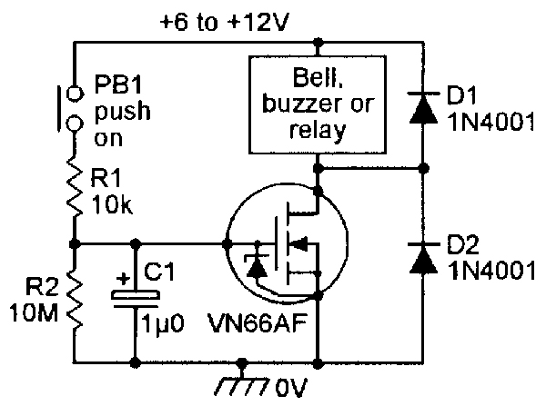
FIGURE 13. Delayed-turn-off power switch. |
In the manually activated delayed-turn-off circuit of Figure 13, C1 charges rapidly via R1 when push-button switch PB1 is closed, and discharges slowly via R2 when PB1 is open. The load thus activates as soon as PB1 is closed, but does not deactivate until some 10s of seconds after PB1 is released.
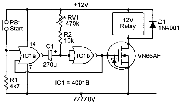
In the simple relay-output timer circuit of Figure 14, the VMOS device is driven by the output of a manually triggered monostable or one-shot multivibrator designed around two gates of a 4001B CMOS IC; the relay turns on as soon as PB1 is closed, and then turns off automatically again some pre-set ‘delay time’ later. The delay is variable from a few seconds to a few minutes via RV1.
 |
 |
| FIGURE 14. Simple relay-output timer circuit. |
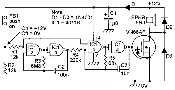
FIGURE 15. Warble-tone six watt alarm. |
Finally, Figure 15 shows the practical circuit of an inexpensive but very impressive alarm-call generator that produces a ‘dee-dah’ sound like that of a British police car siren. The alarm can be turned on by closing PB1 or be feeding a ‘high’ voltage to the R1-R2 junction. The circuit uses an 8R0 speaker and generates roughly six watts of output power.
DC LAMP CONTROLLERS
 |
 |
| FIGURE 16. Simple DC lamp dimmer. |
FIGURE 17. Soft-start lamp switch. |
 |
| FIGURE 18. High-efficiency DC lamp dimmer. |
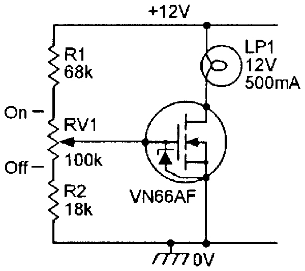
Figures 16 to 18 show three simple but useful DC lamp controller circuits that can be used to control the brilliance of any 12V lamp with a power rating of up to six watts. A VMOS power FET can, for many purposes, be regarded as a voltage controlled constant-current generator; thus, in Figure 16, the VMOS drain current (and thus the lamp brightness) is directly controlled by the variable voltage of RV1’s slider. The circuit thus functions as a manual lamp dimmer.
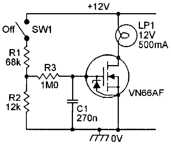
The Figure 17 circuit is a simple modification of the above design, the action being such that the lamp turns on slowly when the switch is closed as C1 charges up via R3, and turns off slowly when the switch is opened as C1 discharges via R3.
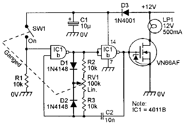
The Figure 18 circuit is an efficient ‘digital’ lamp dimmer which controls the lamp brilliance without causing significant power loss across the VMOS device. The two 4011B CMOS gates form an astable multivibrator with a mark/space ratio that is fully variable from 10:1 to 1:10 via RV1; its output is fed to the VN66AF gate, and enables the mean lamp brightness to be varied from virtually fully-off to fully-on. In this circuit, the VMOS device is alternately switched fully on and fully off, so power losses are negligible.
LINEAR CIRCUITS
VMOS power FETs can, when suitably biased, easily be used in either the common source or common drain (voltage follower) linear modes. The voltage gain in the common source mode is equal to the product of RL and the device’s gM or forward transconductance. In the case of the VN66AF, this gives a voltage gain of 0.25 per ohm of RL value, i.e., a gain of x4 with a 16R load, or x25 with a 100R load. The voltage gain in the common drain mode is slightly less than unity.
A VMOS power FET can be biased into the linear common source mode by using the standard enhancement-mode MOSFET biasing technique shown in Figure 19, in which the R1-R2 potential divider is wired in the drain-to-gate negative feedback loop and sets the quiescent drain voltage at roughly half-supply value, so that maximal signal level swings can be accommodated before clipping occurs.
 |
 |
 |
| FIGURE 19. Biasing technique for linear common source operation. |
FIGURE 20. Biasing techniques for linear common drain (voltage follower) operation. |
FIGURE 21. Simple class-A audio power amplifier gives 1% THD at 1W. |
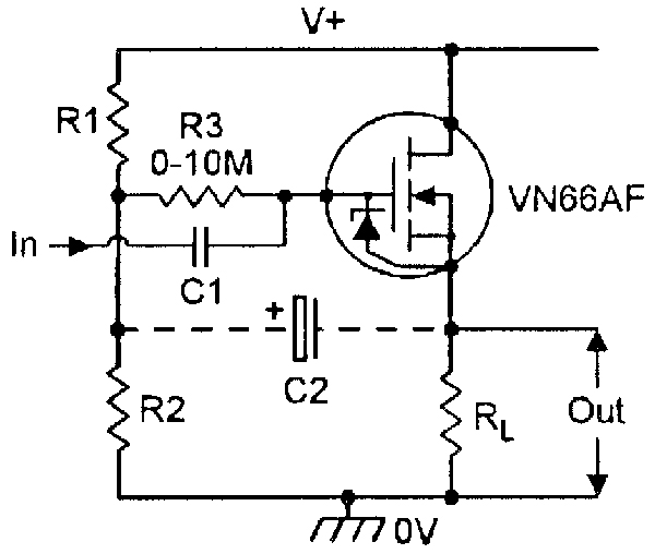
When — in the Figure 19 circuit — R3 has a value of zero ohms, the circuit exhibits an input impedance that, because of the AC negative feedback effects, is roughly equal to the parallel values of R1 and R2 divided by the circuit’s voltage gain (RL x gM. If R3 has a finite value, the input impedance is slightly less than the R3 value, unless AC feedback-decoupling capacitor C2 is fitted in place, in which case, the input impedance is slightly greater than the R3 value.
Figure 20 shows how to bias the VN66AF for common drain (voltage follower) operation. Potential divider R1-R2 sets the VMOS gate at a quiescent value slightly greater than half-supply voltage. When the R3 value is zero, the circuit input impedance is equal to the parallel values of R1 and R2. When the R3 value is finite, the input impedance equals the R3 value plus the parallel R1-R2 values. The input impedance can be raised to a value many times greater than R3 by adding the C2 ‘bootstrap’ capacitor to the circuit.
Finally, Figure 21 shows a practical example of a VMOS linear application. The circuit is wired as a class-A power amplifier which, because of the excellent linearity of the VN66AF, gives remarkably little distortion for so simple a design. The VN66AF must be mounted on a good heatsink in this application. When the design is used with a purely resistive 8R0 load, the amplifier bandwidth extends up to 10MHz. NV
Other Parts In the FET Principles And Circuits Series
FET (Field-Effect Transistor) basics. (Part 1 of 4)
Practical JFET circuits. (Part 2 of 4)
Practical MOSFET and CMOS circuits. (Part 3 of 4)
Practical VMOS power FET circuits aand applications. (Part 4 of 4)