You have found or designed a circuit, and it’s time to build a permanent version of it. You could design and order (or make) a printed circuit board, but that will cost money and/or time. It also makes changes and corrections difficult. The obvious alternative: Implement the circuit on one or several prototyping boards, which have patterns of traces connecting holes on 0.1” centers. Many such boards are available with various patterns of traces at reasonable prices. Several styles are available retail at RadioShack, which fortunately still exists. Figure 1 shows a variety of protoboards.
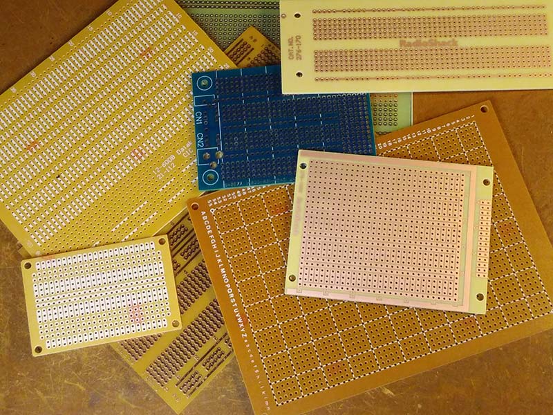
FIGURE 1. A few of the many styles of protoboards.
How do you go about building on a protoboard? I’ll describe a sequence of steps, using the circuit in Figure 2 as an example.
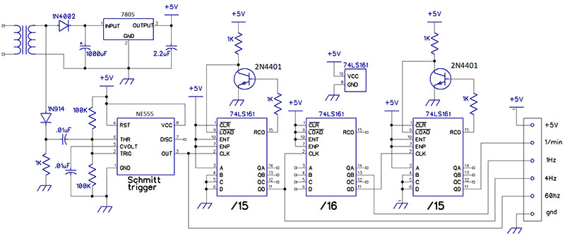
FIGURE 2. A power supply and time base for an old-school digital clock.
The figure presents a power supply and line-frequency-derived time base for a digital clock that uses discrete logic. The circuit is contrived to use a combination of ICs and discrete parts, so provides a better example.
The circuit’s power supply comprises a full-wave rectifier, filter capacitor, and five volt/three-terminal regulator in a conventional arrangement to provide +5V. The time base derives a 60 Hz signal from the line frequency through an NE555-based Schmitt trigger. That signal is used directly for fast setting and is divided to 4 Hz, 1 Hz, and one/minute for slow setting, a blinking colon, and driving the clock’s counters in normal operation.
Transistor inverters send reset signals to two binary counters; they begin their counts at 1 rather than 0, so that they divide their input frequencies by 15. The remaining counter divides its input frequency by 16. (Note that 15 x 16 x 15 = 3600.) Now to building.
Planning
Begin by implementing your circuit on a breadboard, both to examine and verify its performance, and to get some ideas about placing components and connections. Keep the breadboarded circuit intact as a reference during construction and debugging. Figure 3 shows a breadboard of the power supply and time base in Figure 2.
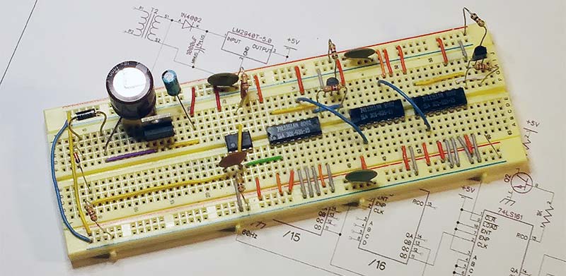
FIGURE 3. A breadboard of the example circuit.
Having verified that the circuit works as intended, select an appropriate protoboard. Consider the size of the board and the pattern of traces it provides. Boards whose component sides indicate their traces are easier to work with than those whose component sides are blank.
On light-colored boards, you can mark traces with a Sharpie or similar marker. This is particularly useful when the board contains busses that can be used for ground and power connections. Dark-colored boards tend not to show such markings well.
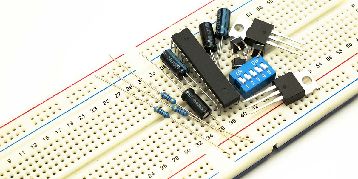
Plan where the larger components will go, with particular attention to ground, +V, and signal paths. Also consider off-board connections: power, signals in and out, and controls. Figure 4 shows a likely arrangement of the major components of the example circuit on a RadioShack board. Note that the board’s two busses have been color-coded red and black for +V and ground, respectively.
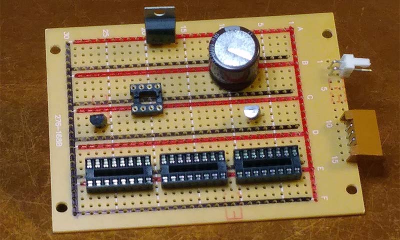
FIGURE 4. Positioning the larger components on the protoboard.
Construction
Now we’re ready to solder. Work from a large copy of the circuit’s schematic and — as each connection is made — keep track of your progress by marking over it with a highlighter or similar marker.
Begin with the larger components. I like to use sockets for DIP integrated circuits; either standard DIP sockets or, if there will be connections or wires under the ICs, two rows of SIP sockets. The resulting construction will be easier to understand and debug if you color-code at least some connections. The most important are +V, which should be red, and ground, which should be black (don’t use those colors for anything else).
Use the same color of wire for all the connections in a given circuit. Figure 5 shows the example board about halfway through its construction, and its schematic at this stage of the process. Some components were moved slightly from their planned positions.
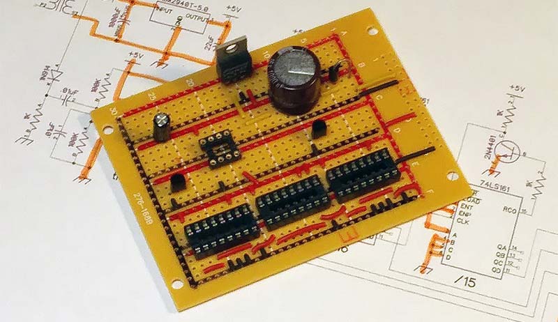
FIGURE 5. The board with major components mounted and about half the wiring done.
Be careful not to run wires over holes you may need to use later. A tiny bend at each end allows a wire to clear intervening holes. In general, short wires are easier to manage than long, and connections can use several steps. Trim wire ends neatly and close to the trace side of the board. Keep the cut-off wires from components like resistors and capacitors; they may be useful in the current project or later.
If possible, once all the ground and +V connections have been made, build and test the circuit in stages. This will make it easier to identify and correct errors. Make short connections before longer ones. Regularly inspect the trace side of the board for solder bridges.
Keep a Record
Throughout the design and construction of your project, take pictures and write regular notes. It may seem that you’ll remember all the details of the process, but six months later, it will be a mystery. Keep your notes in a form you expect to be permanent: in a computer file or on paper. Neatness counts, but not too much; you’re writing for yourself, not for an external audience.
Figure 6 shows the completed example board, resting on the corresponding pages of the notes that describe it.
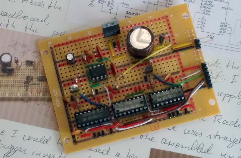
FIGURE 6. The completed board, resting on the corresponding page of notes.
The unit is ready to be used in a complete digital clock.
You will, of course, develop techniques of your own as you design and build — a process in which protoboards are handy and useful tools. Happy building! NV