The only way to avoid ever making a mistake is to do nothing — but that would be a mistake! Just try not to make the same mistakes twice; better yet, learn from someone else’s.
This article is intended to pass along some of the things I learned while designing and developing a Wi-Fi sprinkler project a while back. Some of my errors were outright blunders; some were fairly subtle; and some were tool related. A few might suggest to my alma maters that they reconsider whether granting me my EE degrees was a good idea. Please don’t tell them.
Get the Physical Dimensions Right
If you intend to deploy something that you have designed — like a water sprinkler controller — into a functional role in your household, then to maintain marital harmony your design had better work reliably. That means that some lashed-together prototype board festooned with wires is out; you need a printed circuit board (PCB). If you have not designed one of these before, I encourage you to consider it. They’re really fun, and they don’t cost very much. Using very inexpensive (or free) downloadable software, you “capture” your schematic, map that schematic into a library of parts for their board footprint, place and route the board, then upload that new database to a board fabrication house. For around $100, you can get three boards with your own silkscreening — looking every bit as professional as the commercial boards inside your computer or television.
Despite many verification steps along the way, there are ways to goof up the PCB. One way that I did more than once was to not pay enough attention to the sizes of the holes associated with various components. The DipTrace software that I used for schematic capture and board layout did not have preexisting library entries for the Rabbit Semiconductor RCM5450W wireless module I wanted to use, so I had to create my own. Physically, this module has three bolt holes for the standoffs, and one 50-pin connector on a 0.05” pitch. I wanted to use a through-hole connector (for ease of soldering), so I found such a connector at Mouser and bought a few. Using their datasheets, I drew up the physical component and entered it into my private DipTrace component library. My RCM5450W module footprint looked like Figure 1.
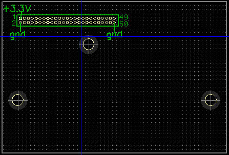
FIGURE 1. RCM5450W module PCB footprint.
On my first board revision, I got the bolt holes exactly in the right places by carefully reading the Rabbit documentation, and also by carefully measuring the actual module with a digital caliper — a procedure I highly recommend. (These calipers are inexpensive and extremely accurate.) However, I generally just eyeballed the hole sizes for the leads on the 50-pin connector, and that was dumb. I did that because when I used this new component in the PCB layout program, I got verification check errors about not enough clearance between the pins. Fixing that issue by shrinking the hole diameters was not my best idea ever. The real connector pins were then exactly the same size as the real holes in the real board, and all 50 pins did not want to go into their respective holes. Respin the PCB: $100.
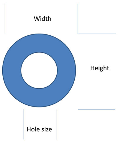
FIGURE 2. PCB through-hole dimensions.
Get the Pins in the Right Places
Then, things got worse. While fixing the hole sizes of the 50-pin connector, I managed to get the two rows of pins interchanged. I think this happened because the default pin numbering facility on my schematic capture software likes to start at pin 1 and number sequentially around the perimeter in a counterclockwise direction, looking down on the component from above. Since Rabbit wants all of the even-numbered pins on one side and odds on the other, I had to manually renumber all the pins, and along the way I accidentally swapped the rows.
Swapping the rows reverses the power and ground connections to the Rabbit module — something Rabbit explicitly warns you not to do. Chips don’t like to be powered up backwards. I once was working next to a technician who had inadvertently reverse-powered all 25 CMOS chips on a board. When he hit the power supply switch for the first time, it was like July 4th fireworks. Chip lids were blasting off and hitting the lab ceiling all over the place, with smoke, flashes, and loud bangs. Fortunately, my Rabbit module took the error in stride while I roundly cursed the dummy (me) who botched the design of this batch of boards. Another $100 mistake.
With the subminiature relays I was using, I not only made the same hole size error, I also didn’t pay enough attention to the fact that these relays were 0.3” wide — pin to pin — not the 0.2” wide that the relay template I was using had assumed. If the holes are too big, that’s generally not a problem, but if they’re too small, it generally is. So, if the spec for a component says its leads have a 0.045” diameter, don’t make the hole 0.045”! Make it slightly bigger. For instance, the 50-pin connector spec says the connector pins are 0.020” in diameter, so I made the PCB holes 0.024” and everything fits great.
Also note that if you set the hole size to be bigger than the width or height, you will have violated the laws of physics, and that never works in your favor.
Board Placement and Routing Dos and Don’ts
I always do board placement manually. There are some provisions in the board layout software for doing auto-place, but I generally have constraints that the program knows nothing about, e.g., where should the wireless module go on the board, if I want its antenna to stick out the top of the chassis in a certain spot. Besides, placement is easy: You just put things where they make logical sense to you. (It’s kinda like when you buy something small and want to know where to keep it. Put it where you would look for it first, in case it goes missing.)
If you possibly can, do a one- or two-layer board because these are significantly cheaper than boards with more layers. Modern boards have a feature called copper fill which lets you fill otherwise unused portions of the PCB with fields of copper that can largely mimic the electrical characteristics of having a true ground plane. If you have a high speed board, you will probably need ground and power planes in it.
The trouble with two-layer boards is that routing all the wires where they need to go can be a challenge, particularly around components with dense pinouts. The RCM5450W, for example, packs 50 pins into a connector with 0.05” pitch which means you cannot route wires between the pins the way you can when the pitch is a more forgiving 0.1”.
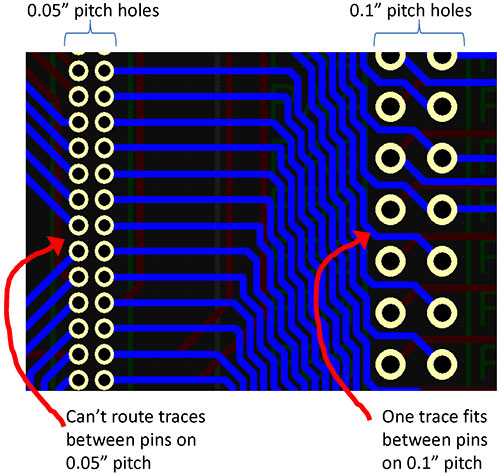
FIGURE 3. Routing between pins.
I also do routing manually. This is related to the two-layer board having no ground plane — there are traces that must be wider than normal signal traces, in order to minimize IR voltage drops for higher currents. I discovered something obvious by doing it the hard way on one board: I auto-routed it, and then hand-edited the result to make sure the fat traces were okay. They weren’t, and it was extremely hard to snake them through the dense underbrush of signals that had been routed hither and yon by the auto-router.
Using the auto-router in that way does not save you any time or effort. It only means you won’t enjoy the experience. Instead, hand-route the power and grounds, and then do any critical signals. Save the resulting file as a checkpoint, then save it again to a new file name. That way, if you don’t like what happens on ensuing steps, it’s easy to get back to the point where power and ground are still the way you wanted them.
I think hand-routing a board is fun. It’s a logical puzzle but with a point: When you’re finished, the result actually does something useful. You can always put jumper wires into your design to “jump over” problem areas, and if you’re going for a one-layer board jumpers will be unavoidable. For two-layer designs, show some pride and design them out.
One of my board revisions came back without the extensive silkscreening I had expected (and paid for). My name wasn’t on the board, nor was the date, board revision, and various labels of switches and other components. It wasn’t the board layout software’s fault. When I entered all that text, I had forgotten to switch that text from the default non-printing layer to the top silkscreen. I did not realize yet one should always check the Gerber output files to make absolutely sure that what you are sending to the PCB fabrication house is what was intended. I do now. The Gerbers are the files that the board fabrication house will actually be using to make your board. Your schematic capture and board layout software probably has a Gerber previewer built in. Use it. If they don’t, there are free Gerber viewers online.
Feature Creep Will Cost You
I had already done several board revisions and debugged them before it dawned on me that without a display on the Wi-Fi Sprinkler (WFS) chassis, there would be no way of telling what state the machine was in by looking at it. If the power was off to the WFS, or its program was malfunctioning, or the wireless wasn’t working, or the home network was down, or the iPod had depleted its batteries, the WFS would not be fulfilling its mission of timed or manual sprinkling, and the user would not know why. LCD modules are cheap and easy to interface to, but I had to again respin the PCB to accommodate this new feature that I should have anticipated from day one.
When I first designed the LCD module in, I figured the software would either be updating the LCD module or sprinkling. I didn’t think I would want to do both at the same time. Later on, I realized I would have to come up with a way to have the WFS do automatic time/date sprinkling, and to do that it would have to know the actual time and date. Using Rabbit example code, I figured out how to use the LCD as a real time clock. But that meant I needed to update the LCD module periodically. If the WFS happened to have a zone sprinkling, it might well sprinkle for 10 or 20 minutes straight. All during that time, port A would not be available to talk to the LCD module. On my last revision of the board, I changed the 4:16 decoder chip to a similar chip with an internal four-bit latch (CD4515). Now, port A could write that latch, and talk to the LCD while the sprinkling continued. I should have worked this all out at the beginning.
I also did not anticipate the need for a 50-pin field of stakes on the board, so that test equipment could readily be attached to known signals on the board. I added this facility after spending many hours with previous revisions of the board, with the usual time wastage associated with connecting a logic analyzer probe to one signal while thinking it was a different one, then wondering why the resulting measurement looked so weird. Thinking ahead to how you’ll debug problems is always a good idea, and will often turn up problems in the design that you can then avoid in the first place. Routing those 50 close pins from the RCM module over to their counterparts on this pin field was a challenge, but I ultimately found a routing pattern that would fit. Silkscreening the name of every pin is a great idea and really cuts down on scope probe placement errors.
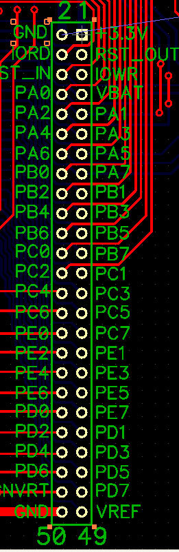
FIGURE 4. Rabbit pins brought to labeled stakes.
Rats, Didn’t See That One Coming
On one revision of the PCB, I had partially populated the board with a few relays and their drivers, and I was wrestling with a peculiar problem: a couple of the relays worked as expected, and a few didn’t. Occasionally, one of the ones that didn’t would chatter and buzz instead of locking in. I wondered if I had miscalculated the base drive resistor values, or if there was a software error, a grounding problem, or the transistors didn’t have the gain I expected. After multiple days of headscratching debug, I finally paid careful attention to what my scope was telling me: Logic lows were as expected, but logic highs into the relay drivers were only 3.3V — not the 5V I had assumed in sizing the resistors. Well, duh ... that’s because my schematic was calling for the CD4515 4:16 decoder chip to run off +3.3V, while the relay driver transistors were connected to +5V. I cut the trace to the 4515 power connection, wired it to +5V, recalculated the base resistor values, and Voila! It was hard for me to see this error because I had assumed one thing while designing the base drive circuit and another thing while drawing up the schematics.
I’ve learned that particular lesson repeatedly in my career: When you’re stuck, it’s always because you’re blinded by some wrong assumption you are making. Question the right assumption, and enlightenment will surely follow.
I remember an incident at Intel when my team was simulating what would eventually become known as the Pentium Pro microprocessor. The man who had written the simulator offhandedly mentioned to me that it was possible to make the simulator initialize flip-flop values pseudo randomly. I said I had been under the assumption we had been testing that way all along. He shrugged and walked away, but the next morning he came back and said he checked; we had not been testing with random initial states, but instead had been simulating our design as though every flip-flop was coming up reset on powerup (which in hardware they most certainly do not). He changed the simulator’s startup configuration to the random initial setting, and re-ran some of the validation regression tests. Many failed. This simple check exposed dozens of design shortcomings that were easy to fix but would potentially have been fatal had they survived into silicon. Assumptions are necessary to make, but some of them will bite you.
Don’t Share Grounds With Noisy Circuits
As Arthur Delagrange said in The Art and Science of Analog Circuit Design, “WARNING: The [board] layout is part of the circuit.” Grounding paths included.
When a relay coil is deasserted, the magnetic field around the coil collapses and induces a current in the coil. That induced current attempts to establish a substantial voltage potential on the transistor’s collector, and a “snubber” diode is connected so as to discharge that current.
However, diodes aren’t perfect. When conducting, silicon diodes drop approximately 0.7 volts across their junctions. That means that the coils can still drive enough current onto their ground connections to make it seem to any logic nearby that ground has dropped by a few tenths of a volt. The Rabbit module itself seemed immune to this, but the LCD module didn’t like it at all and would act as though it had been written with some new value that caused its screen to go blank.
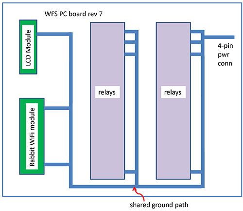
FIGURE 5. Early design with shared grounds.
Figure 5 shows the original ground routing of my rev WFS 7 board. This layout mostly worked. Only when the relay that was electrically farthest from the four-pin power connector at the top right was deactivated, would a large enough current spike occur to cause an LCD module malfunction. The first remedy I tried was to strap a lot of extra ground wires across the top of the board, hoping to drive the aggregate ground impedance down. (This was to gather information only; I would not consider this a permanent fix to a production board, even if it eliminated the problem.)
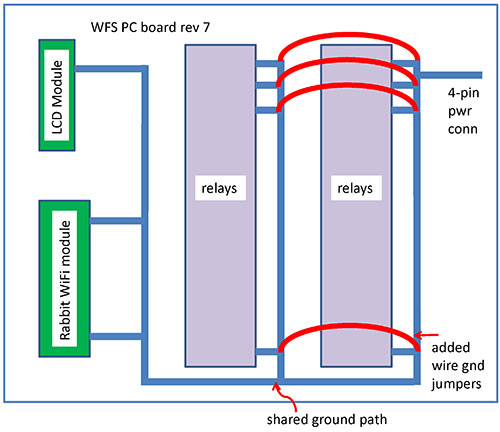
FIGURE 6. Experiment with extra ground straps.
That helped, but the LCD module would still blank out occasionally. So then I got serious, and cut the LCD and Rabbit grounds away from the relays entirely — even at the four-pin power connector. This allowed the relays and the logic to have their own ground current paths all the way back to the power supply itself. With no shared paths, the relays were no longer able to interfere with the logic of the LCD module. Problem solved.
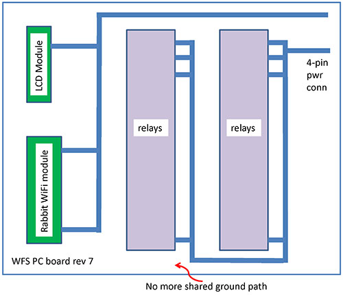
FIGURE 7. Final solution: separate ground paths.
Measure Twice, Cut Once
In woodworking, they have a saying: Measure twice, cut once. The idea is to double-check what you’re about to do because once you’ve cut a board, you can’t uncut it. Don’t take that idea too far though, or you’ll be paralyzed by the fear that you’re overlooking something. Often, you have to simply do your best, fix what didn’t come out right, and keep repeating that loop until you’re finished. If you never make a mistake, you’re not trying hard enough.
Getting better at your craft requires that you learn from mistakes. If you really want to accelerate your learning, learn from other people’s mistakes too! NV
