The secret to getting the most bang for your buck and performance is using the proper circuit topology for your particular application.
There are many types of oscillators used for many different applications. From motor speed control to light dimming, to switching power supplies, to RF broadcasting, to fiber optic data transmission, and on and on. The 555 timer IC is a low cost circuit used to generate PWM (pulse width modulation) clock pulses when used in its astable oscillator mode. It is used for car turn signals, flashing lights, and a myriad of other applications.
There is one problem with the 555 that to me renders the part useless in PWM applications. It can never always be 100% off or on. At best, its range is about 1% to 99%. So, a motor or light can never be completely off or on. That is terrible!
There is a much better solution in an eight-pin package that provides maximum on and off control, PWM modulation, FM modulation, and many more features. What is this magical IC, you ask? It is a dual op-amp chip such as the LM358 or MCP6022.
We’ll explore and analyze several circuits and their applications in this article to show how effective and easy it is to design and use this circuit topology. Let’s begin by looking at the circuit in Figure 1.
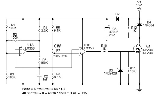
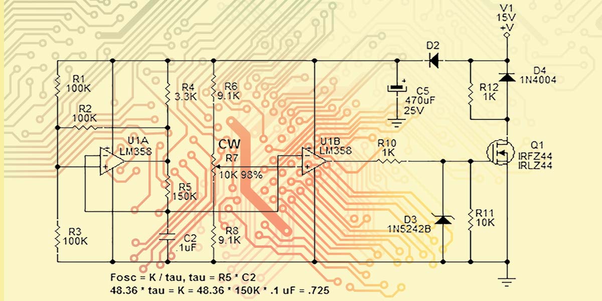
FIGURE 1.
The heart of the oscillator is U1A, R1-R5, and C2. R1 and R3 divide the V1 supply voltage in half, and their combined resistance is R1*R3/(R1 + R3) = 50K. Since R2 = 100K, when the output of U1A switches from ground to 15 volts (+V1), the junction of U1A+ and R1-R2-R3 switches from five volts to 10 volts. R5 starts charging C2. When C2 charges above 10 volts, the input of U1A- is higher than U1A+. That causes the output of U1A to switch to zero volts.
In turn, the junction of U1A+ and R1-R2-R3 switches from 10 volts to five volts. R5 begins to discharge C2. When C2 discharges below five volts, the input of U1A- is lower than U1A+. The output of U1A switches from zero volts to 15 volts (+V1), and the junction of U1A+ and R1-R2-R3 switches from five volts to 10 volts. R5 begins to charge C2 and the cycle keeps repeating. C2 is constantly ramping up and down between +V1*1/3 (5V) and +V1*2/3 (10V).
The really cool thing is that this circuit oscillates at the same frequency even if the supply voltage +V1 changes! That is one of the big features of the 555. U1B acts as a comparator to provide the 0% to 100% PWM output. R6, R7, and R8 form a resistive divider. Notice that R6 and R8 are 10% lower resistance than potentiometer R7. Doing the math, 15*(R7 + R8)/(R6 + R7 + R8) = 15*19.1K/ (28.2K) = 10.16 volts at full clockwise (100% on), and 15*R8/(R6 + R7 + R8) = 15*9.1/28.2 = 4.84 volts at full counter-clockwise (0% off).
The U1B- input is connected to the junction of R5 and C2 which ramps up and down between five and 10 volts. U1B+ is connected to the wiper on potentiometer R7. Whenever the ramp voltage is higher than the wiper reference voltage, the output of U1B goes high; whenever the ramp voltage is lower than the wiper reference voltage, the output of U1B is low. Since the wiper reference voltage can be set higher than the highest ramp voltage, 100% on time is possible.
Additionally, since the wiper reference voltage can be set lower than the lowest ramp voltage, 0% on time (100% off) is possible. This cannot be done with a 555 timer. So, off can really be off, and on can be full on.
The output of U1B is connected to a switch to power the load. In Figure 1, the output is connected via R10 to the gate of Q1 which is an IRLZ44 MOSFET transistor. D3 and R11 protect the gate of Q1 from being over-driven with voltage. R12 provides a light resistive load to Q1, while D4 protects Q1 from inductive load voltage spikes. An alternate design is shown in Figure 2 with a current mirror-limit formed with R12, R13, R14, and transistors Q2, Q3, and Q4. With R12 and R14 equal to 20 ohms, the current to the LED strings composed of D4-6 and D7-9 is .6V/20 or 30 mA.

FIGURE 2. LED light dimmer application with on/off fade.
The two strings of LEDs use about 60 mA total. Resistor R10 feeds Q1 that is used as a bipolar switch. With the oscillator frequency set at 322 Hz, there is no visible flicker and the duty cycle of the PWM output effectively dims the LED’s brightness.
Notice too, that S1, R9, and C3 have been added to the circuit. When S1 is open, the wiper reference voltage changes very slowly as R7 is adjusted up or down, providing a slow fading effect. If used with a motor — such as on a model railroad train — the effect is slow acceleration or a momentum effect. Such a circuit is shown in Figure 3.
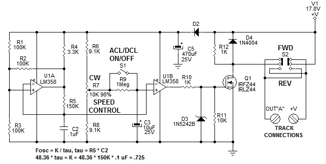
FIGURE 3. Motor speed control application with ACL/DCL.
Switch S2 provides the forward/reverse polarity function. The ACL/DCL time constant (set by R9 and C3) is around 30 seconds. That is the time needed to accelerate to full speed or decelerate to a stop.
Figure 4 shows an IR transmitter application.
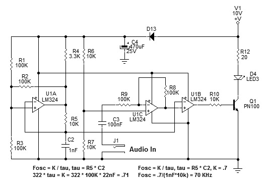
FIGURE 4. PWM modulated oscillator circuit.
The PWM is modulated by U1C. As the audio input varies, U1C acts as an inverting buffer, centered at V1/2 (2.5V). The changing input voltage causes the reference voltage at U1B+ to change. U1B- is varying from V1/3 to V1*2/3. The output of U1B therefore varies in duty cycle from 0% to 100%, depending on the amplitude of the audio input. By making the frequency very high (50 kHz to 100 kHz), the PWM beam of light can carry the audio input signal information. This works like AM radio modulation. The output wave form is shown in Figure 4A. Notice how the on and off times vary as the audio varies.
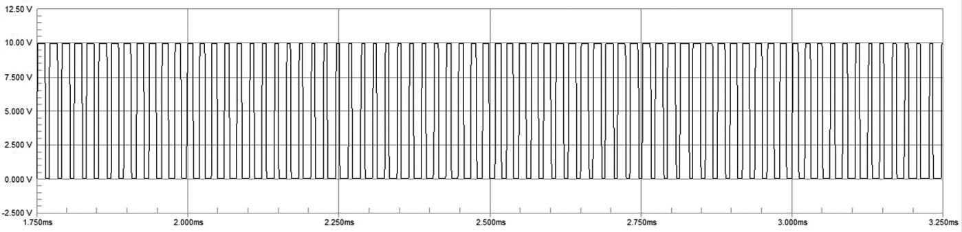
FIGURE 4A. Modulated PWM waveform.
A receiver (refer to Figure 5) that detects the IR beam can recover the information by amplifying the signal and processing it using a low pass filter (integrator) — much like an AM radio signal is recovered.
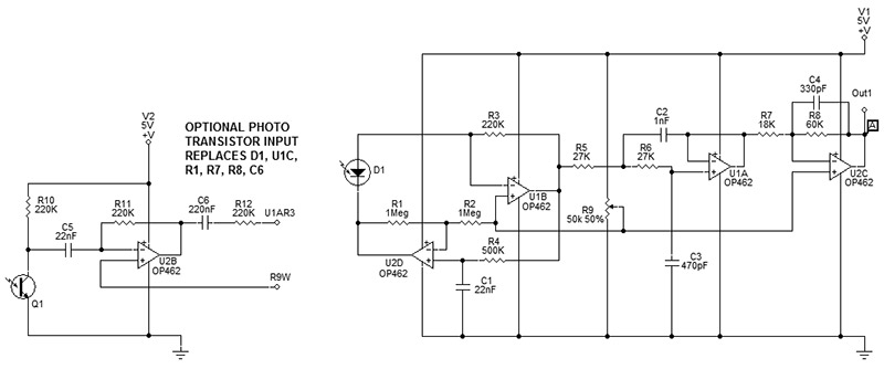
FIGURE 5. Optical detector with 8.6 kHz low pass filter.
The on time of the light pulse is similar to the amplitude of the RF envelope of an AM radio signal.
By modifying the oscillator circuit as shown in Figure 6, it is possible to FM (frequency modulate) the IR oscillator.
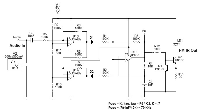
FIGURE 6. FM modulated oscillator circuit with IR output.
The resulting modulation and output waveforms are shown in Figure 6A and 6B.
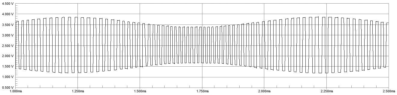
FIGURE 6A. Signal at U1C+ input.
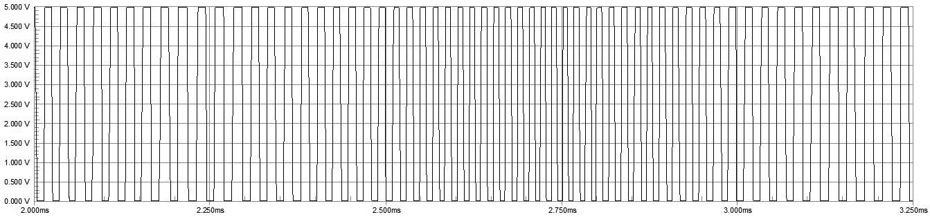
FIGURE 6B. Signal at U1C output.
The circuit operation can best be described as follows.
Resistor R9, R10, and R11 form a 2Vs/3 and Vs/2 divider reference to U1A and U1B. Therefore, the output of U1B is 2Vs/3. Since U1A references the Vs/2 point, has a gain of -1, and is connected to the output of U1B (U1B is Vs/6 above Vs/2), the output of U1A is Vs/3.
When a signal is fed through C2 to U1B and the audio gets more positive, the output of U1B decreases and the output of U1A increases.
Since the reference points for oscillator U1C are closer together, the frequency increases.
Likewise, when the signal to U1B goes negative, the output of U1B increases and the output of U1A decreases. Since the reference points for oscillator U1C are farther apart, the frequency decreases. This is clearly seen in Figure 6A. The output from U1C is shown in Figure 6B.
The amplitude is always rail-to-rail/on and off, but the frequency changes based on the audio input signal. Diodes D1 and D2 make sure that the opposite polarity reference is used each time the U1C output switches from low to high or high to low.
The U1C output is fed to Q1-Q2 which forms a current mirror. R13 limits the current through Q2 to approximately 25-30 mA to drive the IR LED LD1. The current mirror assures that the LED output will be constant regardless of temperature or battery voltage (Vs).
The IR receiver shown in Figure 7 is used to recover the original audio signal.

FIGURE 7. IR FM receiver using CD4046 PLL.
The received FM pulses are fed to a PLL (Phase Locked Loop) such as a CD4046. The PLL tries to match its frequency to the frequency of the incoming IR pulses. The phase error correction signal changes the local oscillator to match the incoming frequency.
The error correction signal is the same as the original audio signal which can be amplified and sent to a speaker.
Another use for the IR transmitter-receiver pair is for remote listening. To demonstrate this technique, get a small speaker and place a layer of aluminum foil over the frame of the speaker. Connect the speaker to an amplifier and play some music or a voice recording. Point the IR transmitter at the speaker. Do not connect any audio to the transmitter input. This gives a constant output frequency. Point the IR receiver at the speaker.
As the speaker diaphragm vibrates back and forth, so will the aluminum foil. As the IR waves reflect off of the aluminum foil, they will be frequency modulated by the vibrations due to the Doppler effect. The IR receiver will try to match the local PLL oscillator frequency to that of the incoming IR pulses, and you will hear the audio via the reflected IR beam.
Spies have used this technique to eavesdrop on conversations through windows which vibrate when sounds are made inside a room. They can remotely hear the conversation because of the vibrations of the window glass. (This would make a great science fair project.)
Now, with this information, you should be able to make light dimmers, PWM motor speed controllers, model train controllers, AM and FM modulated transmitters and receivers, heater controls, and a host of other applications. NV