The opening episode of this four-part ‘op-amp’ series described the basic operating principles of conventional voltage-differencing op-amps (typified by the 741 type) and showed some basic circuit configurations in which they can be used.
This month’s concluding episode looks at practical ways of using such op-amps in various instrumentation and test-gear applications, including those of precision rectifiers, AC/DC converters, electronic analog meter drivers, and variable voltage-reference and DC power supply circuits.
When reading this episode, note that most practical circuits are shown designed around a standard 741, 3140 ,or LF351-type op-amp and operated from dual 9V supplies, but that these circuits will usually work (without modification) with most voltage-differencing op-amps, and from any DC supply within that op-amp’s operating range. Also note that all 741-based circuits have a very limited frequency response, which can be greatly improved by using an alternative ‘wide-band’ op-amp type.
ELECTRONIC RECTIFIER CIRCUITS
Simple diodes are poor rectifiers of low-level AC signals, and do not start to conduct until the applied voltage exceeds a certain ‘knee’ value; silicon diodes have knee values of about 600mV, and thus give negligible rectification of signal voltages below this value. This weakness can be overcome by wiring the diode into the feedback loop of an op-amp, in such a way that the effective knee voltage is reduced by a factor equal to the op-amp’s open-loop voltage gain; the combination then acts as a near-perfect rectifier that can respond to signal inputs as low as a fraction of a millivolt. Figure 1 shows a simple half-wave rectifier of this type.
 |
| FIGURE 1. Simple half-wave rectifier circuit. |
The Figure 1 circuit is wired as a non-inverting amplifier with feedback applied via silicon diode D1, and with the circuit output taken from across load resistor R1. When positive input signals are applied to the circuit, the op-amp output also goes positive; an input of only a few microvolts is enough to drive the op-amp output to the 600mV ‘knee’ voltage of D1, at which point, D1 becomes forward biased. Negative feedback through D1 then forces the inverting input (and thus the circuit’s output) to accurately follow all positive input signals greater than a few microvolts. The circuit thus acts as a voltage follower to positive input signals.
When the input signal is negative, the op-amp output swings negative and reverse biases D1. Under this condition, the reverse leakage resistance of D1 (typically hundreds of megohms) acts as a potential divider with R1 and determines the negative voltage gain of the circuit; typically, with the component values shown, the negative gain is roughly -60dB. The circuit thus ‘follows’ positive input signals but rejects negative ones, and hence acts like a near-perfect signal rectifier.
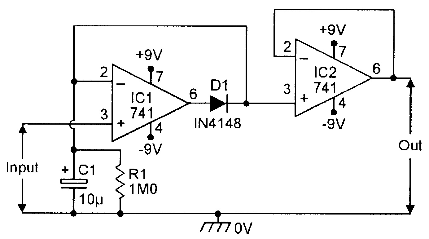 |
| FIGURE 2. Peak detector with buffered output. |
Figure 2 shows how the above circuit can be modified to act as a peak voltage detector by wiring C1 in parallel with R1. This capacitor charges rapidly, via D1, to the peak positive value of an input signal, but discharges slowly via R1 when the signal falls below the peak value. IC2 is used as a voltage-following buffer stage, to ensure that R1 is not shunted by external loading effects.
Note that the basic Figure 1 and 2 circuits each have a very high input impedance. In most practical applications, the input signal should be AC-coupled and pin 3 of the op-amp should be tied to the common rail via a 100k resistor.
PRECISION RECTIFIER CIRCUITS
The Figure 1 rectifier circuit has a rather limited frequency response, and may produce a slight negative output signal if D1 has poor reverse resistance characteristics. Figure 3 shows an alternative type of half-wave rectifier circuit, which has a greatly improved rectifier performance at the expense of a greatly reduced input impedance.
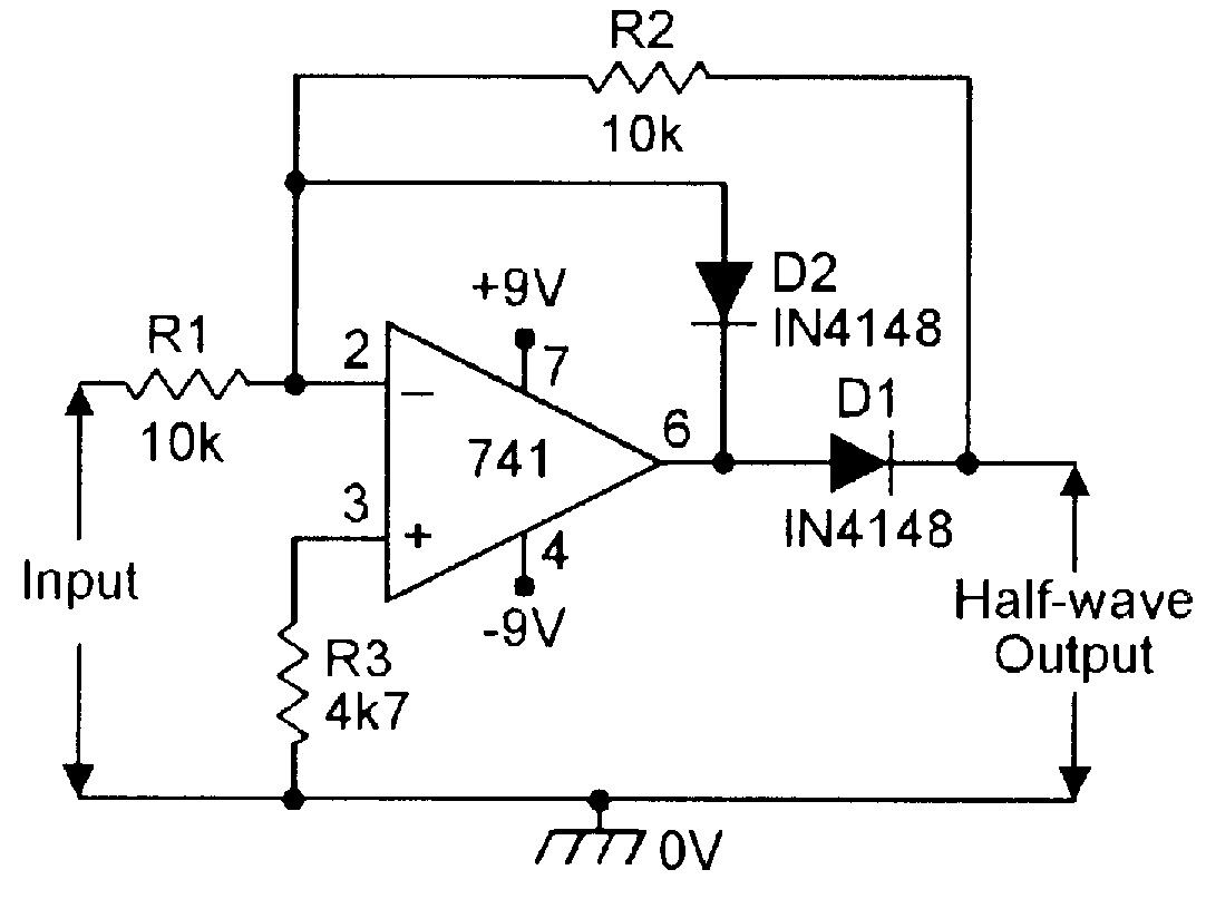 |
| FIGURE 3. Precision half-wave rectifier. |
In Figure 3, the op-amp is wired as an inverting amplifier with a 10k (= R1) input impedance. When the input signal is negative, the op-amp output swings positive, forward biasing D1 and developing an output across R2. Under this condition the voltage gain equals (R2+RD)/R1, where RD is the active resistance of this diode. Thus, when D1 is operating below its knee value its resistance is large and the circuit gives high gain, but when D1 is operating above the knee value its resistance is very low and the circuit gain equals R2/R1. The circuit thus acts as an inverting precision rectifier to negative input signals.
When the input signal goes positive, the op-amp output swings negative, but the negative swing is limited to -600mV via D2, and the output at the D1-R2 junction does not significantly shift from zero under this condition. This circuit thus produces a positive-going half-wave rectified output. The basic circuit can be made to give a negative-going half-wave rectified output by simply reversing the polarities of the two diodes.
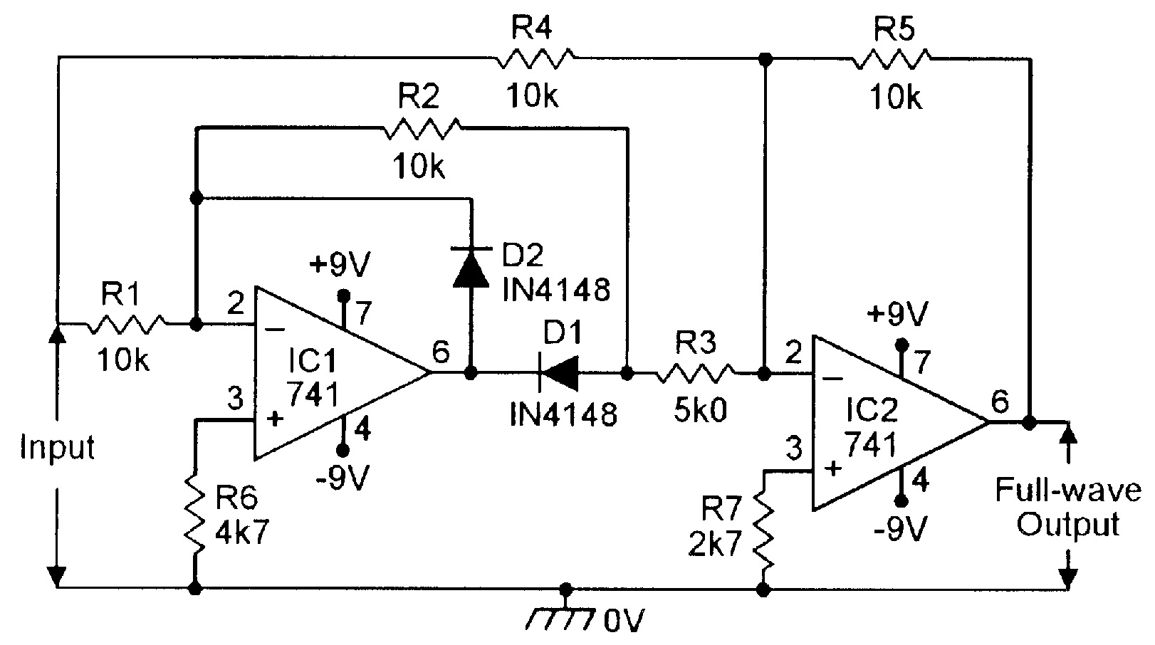 |
| FIGURE 4. Precision full-wave rectifier. |
Figure 4 shows how a negative-output version of the above circuit can be combined with an inverting ‘adder’ to make a precision full-wave rectifier. Here, IC2 inverts and gives x2 gain (via R3-R5) to the half-wave rectified signal of IC1, and inverts and gives unity gain (via R4-R5) to the original input signal (Ein). Thus, when negative input signals are applied, the output of IC1 is zero, so the output of IC2 equals +Ein. When positive input signals are applied, IC1 gives a negative output, so IC2 generates an output of +2Ein via IC1 and -Ein via the original input signal, thus giving an actual output of +Ein. The output of this circuit is thus positive, and always has a value equal to the absolute value of the input signal.
AC/DC CONVERTER CIRCUITS
The Figure 3 and 4 circuits can be made to function as precision AC/DC converters by first providing them with voltage-gain values suitable for form-factor correction, and by then integrating their outputs to give the AC/DC conversion, as shown in Figures 5 and 6, respectively. Note that these circuits are intended for use with sinewave input signals only.
 |
| FIGURE 5. Precision half-wave AC/DC converter. |
In the half-wave AC/DC converter in Figure 5, the circuit gives a voltage gain of x2.22 via R2/R1, to give form-factor correction, and integration is accomplished via C1-R2. Note that this circuit has a high output impedance, and the output must be buffered if it is to be fed to low-impedance loads.
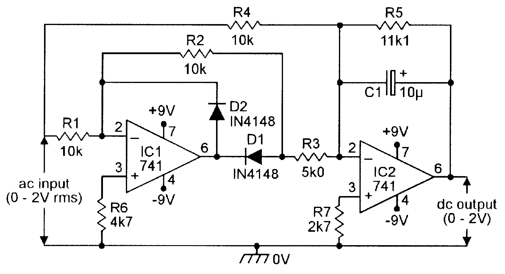 |
| FIGURE 6. Precision full-wave AC/DC converter. |
In the full-wave AC/DC converter in Figure 6, the circuit has a voltage gain of x1.11 to give form-factor correction, and integration is accomplished via C1-R5. This circuit has a low-impedance output.
DVM CONVERTER CIRCUITS
Precision 3-1/2 digit Digital Voltmeter (DVM) modules are readily available at modest cost, and can easily be used as the basis of individually-built multi-range and multi-function meters. These modules are usually powered via a 9V battery, and have a basic full-scale measurement sensitivity of 200mV DC and a near-infinite input resistance. They can be made to act as multi-range DC voltmeters by simply feeding the test voltage to the module via a suitable ‘multiplier’ (resistive attenuator) network, or as multi-range DC current meters by feeding the test current to the module via a switched current shunt.
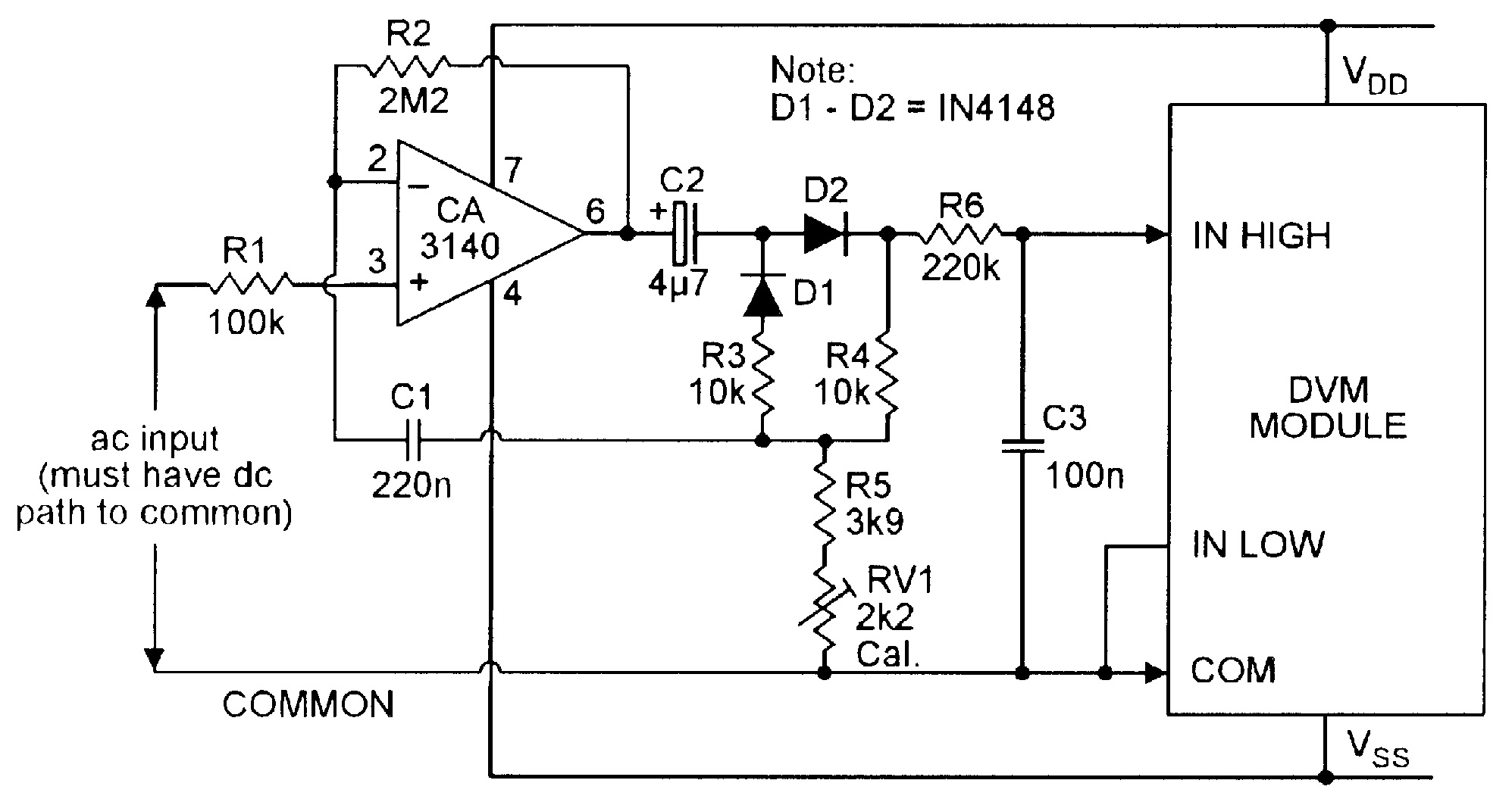 |
| FIGURE 7. AC/DC converter for use with DVM module. |
A DVM module can be used to measure AC voltages by connecting a suitable AC/DC converter to its input terminals, as shown in Figure 7. This particular converter has a near-infinite input impedance. The op-amp is used in the non-inverting mode, with DC feedback applied via R2 and AC feedback applied via C1-C2 and the diode-resistor network.
The converter gain is variable over a limited range (to give form-factor correction) via RV1, and the circuit’s rectified output is integrated via R6-C3, to give DC conversion. The COMMON terminal of the DVM module is internally biased at about 2.8 volts below the VDD (positive supply terminal) voltage, and the CA3140 op-amp uses the VDD, COMMON, and VSS terminals of the module as its supply rail points.
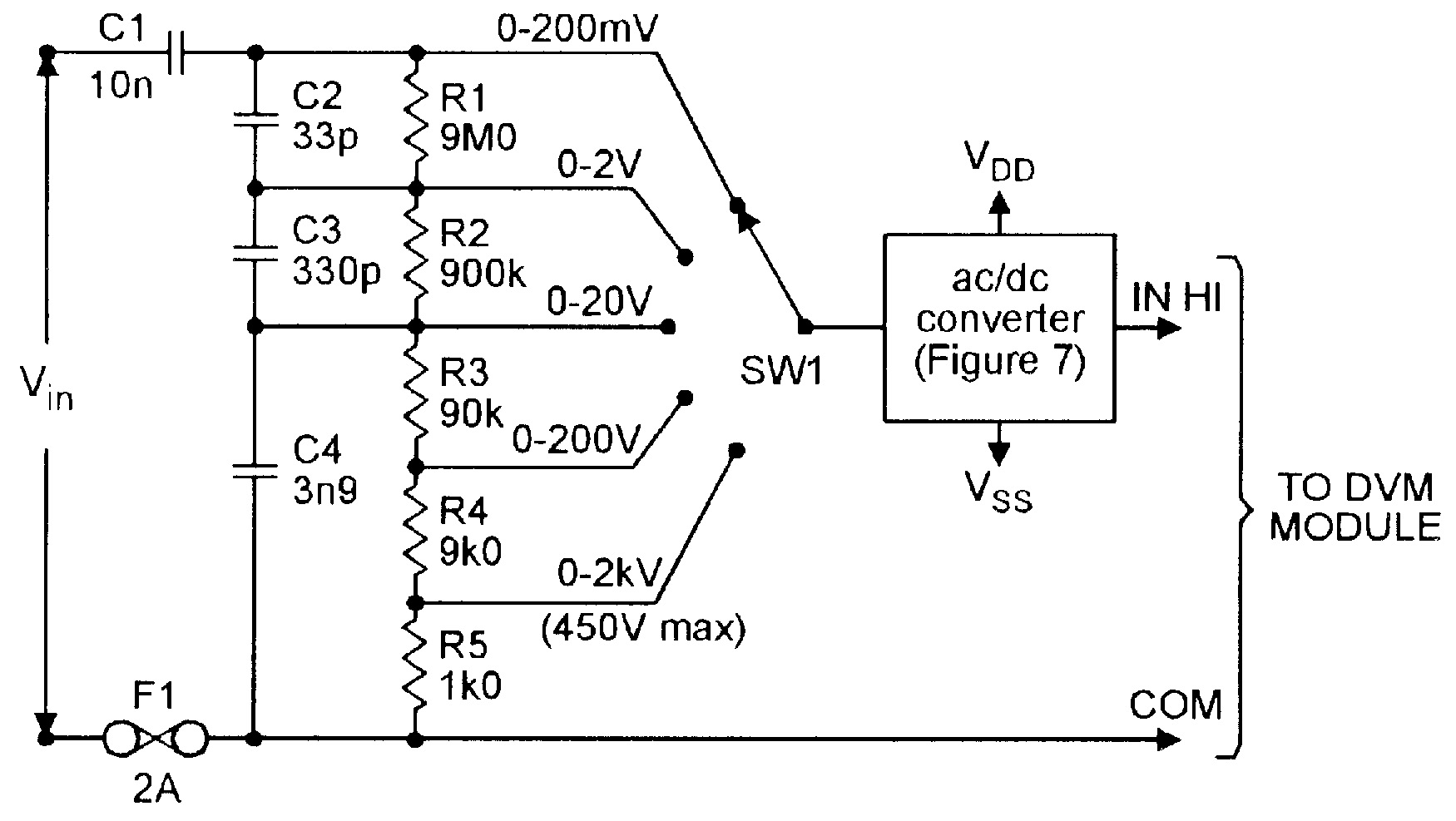 |
| FIGURE 8. Five-range AC voltmeter converter for use with DVM modules. |
Figure 8 shows a simple frequency-compensated attenuator network used in conjunction with the above AC/DC converter to convert a standard DVM module into a five-range AC voltmeter, and
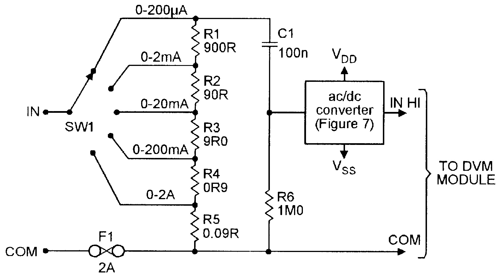 |
| FIGURE 9. Five-range AC current-meter converter for use with DVM modules. |
Figure 9 shows how a switched shunt network can be used to convert the module into a five-range AC current meter.
 |
| FIGURE 10. Five-range ohmmeter converter for use with DVM modules. |
Figure 10 shows a circuit that can be used to convert a DVM module into a five-range ohmmeter. This circuit actually functions as a multi-range constant-current generator, in which the constant current feeds (from Q1 collector) into RX, and the resulting RX volt drop (which is directly proportional to the RX value) is read by the DVM module.
Here, Q1 and the op-amp are wired as a compound voltage follower, in which Q1 emitter precisely follows the voltage set on RV1 slider. In practice, this voltage is set at exactly 1V0 below VDD, and the emitter and collector (RX) currents of Q1 thus equal 1V0 divided by the R3 to R7 range-resistor value, e.g., 1mA with R3 in circuit, etc. The actual DVM module reads full scale when the RX voltage equals 200mV, and this reading is obtained when RX has a value one-fifth of that of the range resistor, e.g., 200R on Range 1, or 2M0 on Range 5, etc.
ANALOG METER CIRCUITS
An op-amp can easily be used to convert a standard moving coil meter into a sensitive analog voltage, current, or resistance meter, as shown in the practical circuits of Figures 11 to 16. All six circuits operate from dual 9V supplies and are designed around the LF351 JFET op-amp, which has a very high input impedance and good drift characteristics. All circuits have an offset nulling facility, to enable the meter readings to be set to precisely zero with zero input, and are designed to operate with a moving coil meter with a basic sensitivity of 1mA fsd.
If desired, these circuits can be used in conjunction with the 1mA DC range of an existing multi-meter, in which case, these circuits function as ‘range converters.’ Note that each circuit has a 2k7 resistor wired in series with the output of its op-amp, to limit the available output current to a couple of milliamps and thus provide the meter with automatic overload protection.
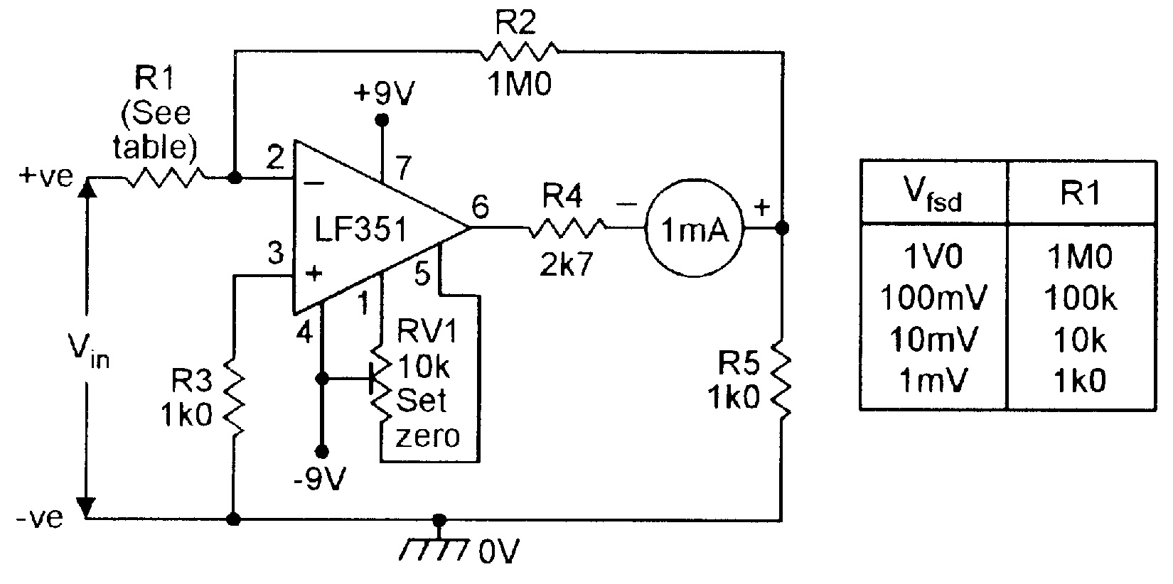 |
| FIGURE 11. A DC millivoltmeter circuit. |
Figure 11 shows a simple way of converting the 1mA meter into a fixed-range DC millivolt meter with a full-scale sensitivity of 1mV, 10mV, 100mV, or 1V0. The circuit has an input sensitivity of 1M0/volt, and the table shows the appropriate R1 value for different fsd sensitivities. To set the circuit up initially, short its input terminals together and adjust RV1 to give zero deflection on the meter. The circuit is then ready for use.
 |
| FIGURE 12. A DC voltage or current meter. |
Figure 12 shows a circuit that can be used to convert a 1mA meter into either a fixed-range DC voltmeter with any full-scale sensitivity in the range 100mV to 1000V, or a fixed-range DC current meter with a full-scale sensitivity in the range 1µA to 1A. The table shows alternative R1 and R2 values for different ranges.
 |
| FIGURE 13. Four-range DC millivoltmeter. |
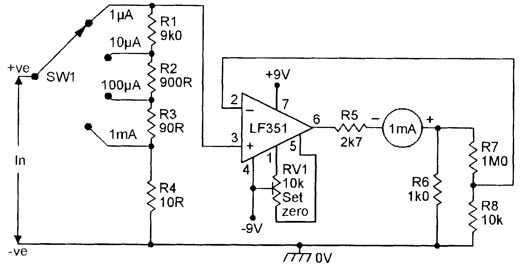
Figure 13 shows how the above circuit can be modified to make a four-range DC millivolt meter with fsd ranges of 1mV, 10mV, 100mV, and 1V0, and Figure 14 shows how it can be modified to make a four-range DC microammeter with fsd ranges of 1µA, 10µA, 100µA, and 1mA. The range resistors used in these circuits should have precisions of 2% or better.
 |
|
| FIGURE 14. Four-range DC microammeter. |
|
Figure 15 shows the circuit of a simple but very useful four-range AC millivoltmeter. The input impedance of the circuit is equal to R1, and varies from 1k0 in the 1mV fsd mode to 1M0 in the 1V fsd mode. The circuit gives a useful performance at frequencies up to about 100kHz when used in the 1mV to 100mV fsd modes. In the 1V fsd mode, the frequency response extends up to a few tens of kHz. This good frequency response is ensured by the LF351 op-amp, which has very good bandwidth characteristics.
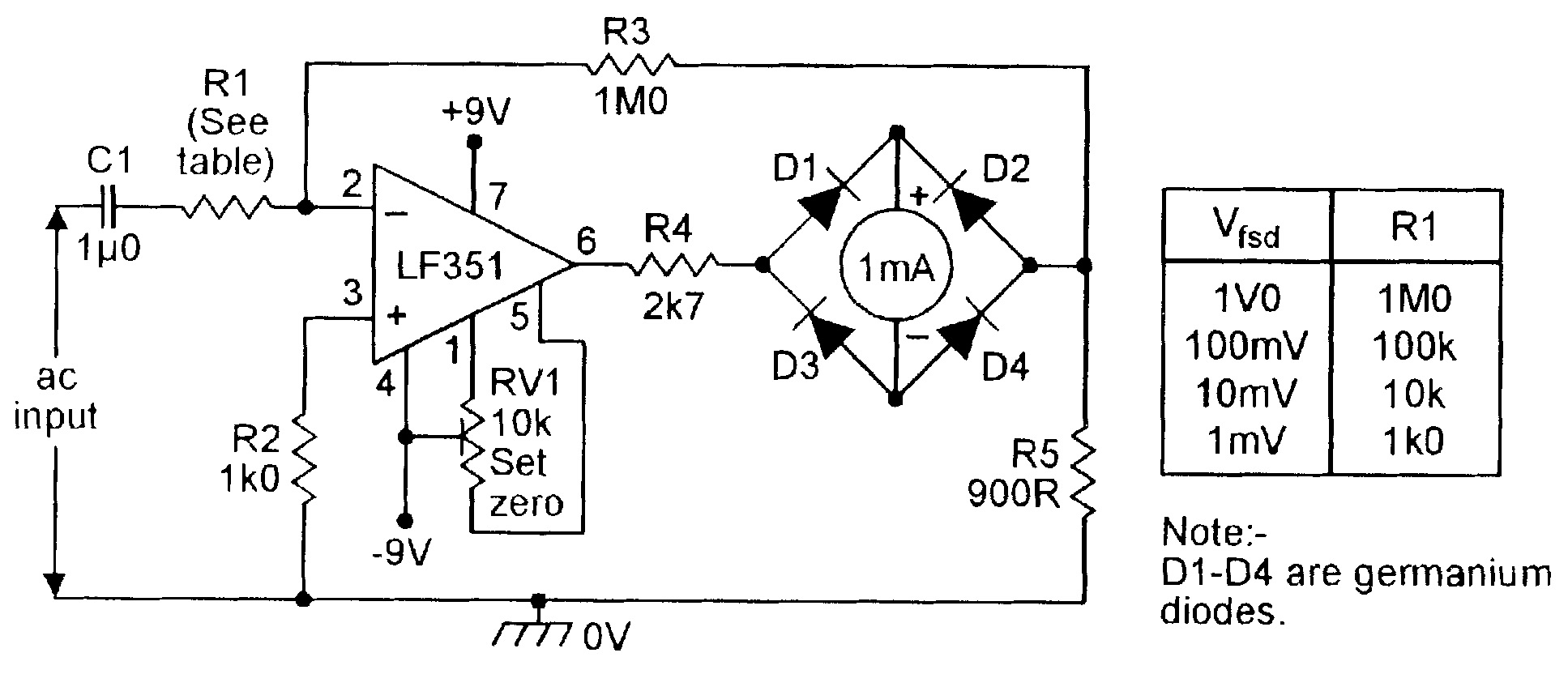 |
| FIGURE 15. Four-range AC millivoltmeter. |
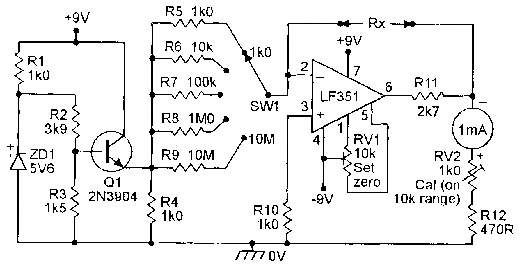
Finally, Figure 16 shows the circuit of a five-range linear-scale ohmmeter, which has full-scale sensitivities ranging from 1k0 to 10M. Range resistors R5 to R9 determine the measurement accuracy. Q1-ZD1 and the associated components simply apply a fixed 1V0 (nominal) to the ‘common’ side of the range-resistor network, and the gain of the op-amp circuit is determined by the ratios of the selected range-resistor and RX and equals unity when these components have equal values. The meter reads full-scale under this condition, since it is calibrated to indicate full-scale when 1V0 (nominal) appears across the RX terminals.
 |
| FIGURE 16. Five-range linear-scale ohmmeter. |
To initially set up the Figure 16 circuit, set SW1 to the 10k position and short the RX terminals together. Then adjust the RV1 ‘set zero’ control to give zero deflection on the meter. Next, remove the short, connect an accurate 10k resistor in the RX position, and adjust RV2 to give precisely full-scale deflection on the meter. The circuit is then ready for use, and should need no further adjustment for several months.
VOLTAGE REFERENCE CIRCUITS
An op-amp can be used as a fixed or variable voltage reference by wiring it as a voltage follower and applying a suitable reference to its input. An op-amp has a very high input impedance when used in the ‘follower’ mode and thus draws near-zero current from the input reference, but has a very low output impedance and can supply several milliamps of current to an external load. Variations in output loading cause little change in the output voltage value.
 |
| FIGURE 17. Variable positive voltage reference. |
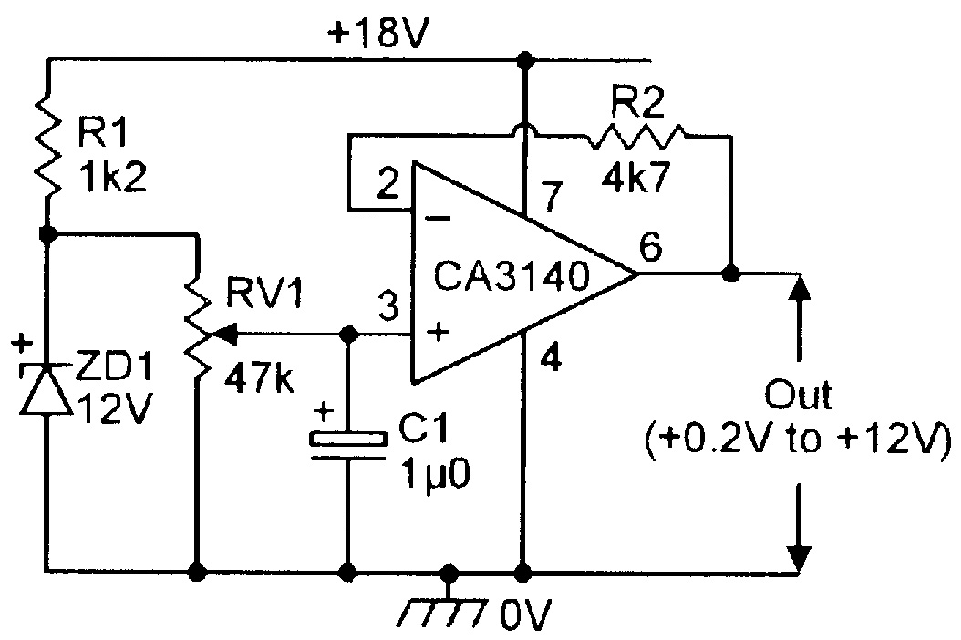
Figure 17 shows a practical positive voltage reference with an output fully variable from +0.2V to +12V via RV1. Zener diode ZD1 generates a stable 12V, which is applied to the non-inverting input of the op-amp via RV1. A CA3140 op-amp is used here because its input and output can track signals to within 200mV of the negative supply rail voltage. The complete circuit is powered from an unregulated single-ended 18V supply.
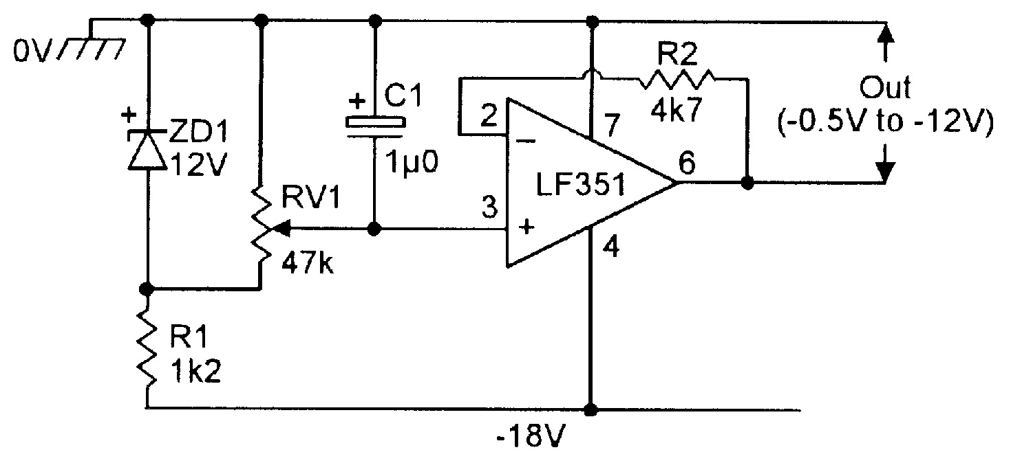 |
| FIGURE 18. Variable negative voltage reference. |
Figure 18 shows a negative voltage reference that gives an output fully variable from -0.5V to -12V via RV1. An LF351 op-amp is used in this design, because its input and output can track signals to within about 0.5V of the positive supply rail value. Note that the op-amps used in these two regulator circuits are wide-band devices, and R2 is used to enhance their circuit stability.
VOLTAGE REGULATOR CIRCUITS
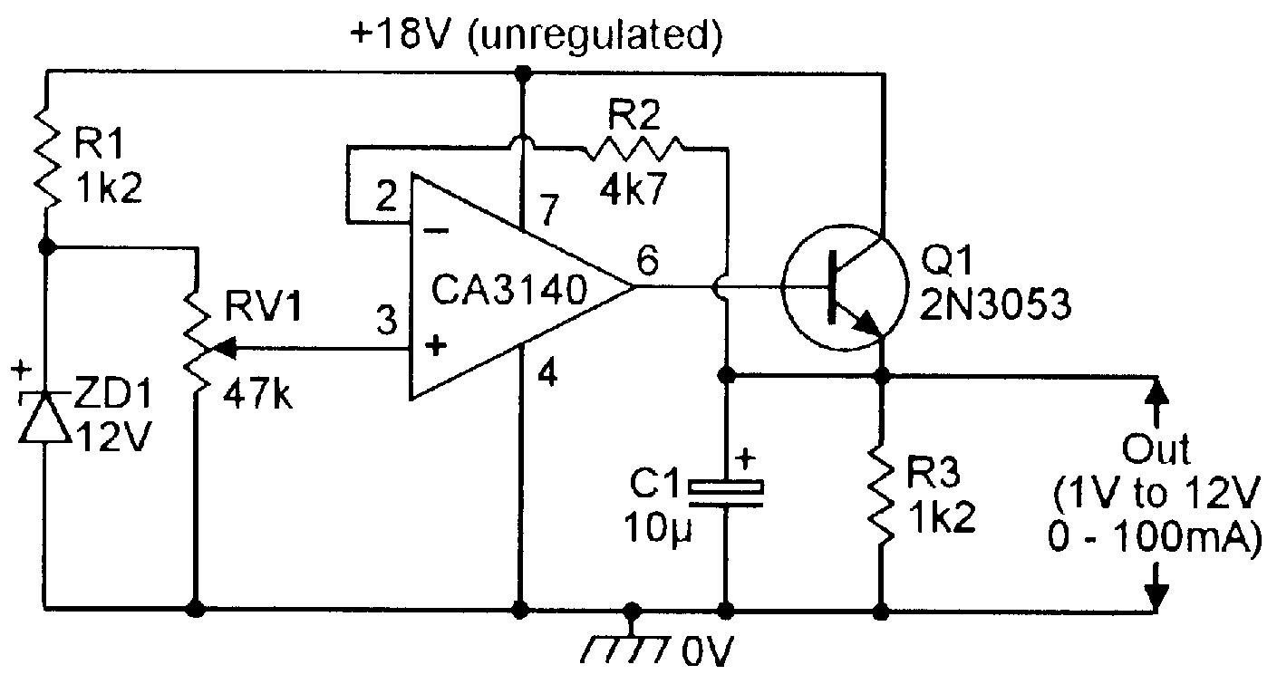
The basic circuits in Figures 17 and 18 can be made to act as high-current regulated voltage (power) supply circuits by wiring current-boosting transistor networks into their outputs.
 |
| FIGURE 19. Simple variable-voltage regulated power supply. |
Figure 19 shows how the Figure 17 circuit can be modified to act as a 1V to 12V variable power supply with an output current capability (limited by Q1’s power rating) of about 100mA. Note that the base-emitter junction of Q1 is included in the circuit’s negative feedback loop, to minimize offset effects. The circuit can be made to give an output that is variable all the way down to zero volts by connecting pin 4 of the op-amp to a supply that is at least 2V negative.
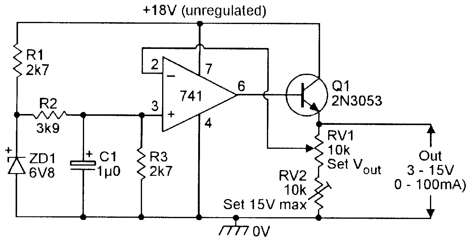 |
| FIGURE 20. 3V to 15V, 0 to 100 mA stabilized PSU. |
Figure 20 shows an alternative type of power supply circuit, in which the output is variable from 3V to 15V at currents up to 100mA.
In this case, a fixed 3V reference is applied to the non-inverting input terminal of the 741 op-amp via ZD1 and the R2-C1-R3 network, and the op-amp plus Q1 are wired as a non-inverting amplifier with gain variable via RV1.
When RV1 slider is set to the upper position, the circuit gives unity gain and gives an output of 3V; when RV1 slider is set to the lower position the circuit gives a gain of x5 and thus gives an output of 15V. The gain is fully variable between these two values. RV2 enables the maximum output voltage to be pre-set to precisely 15V.
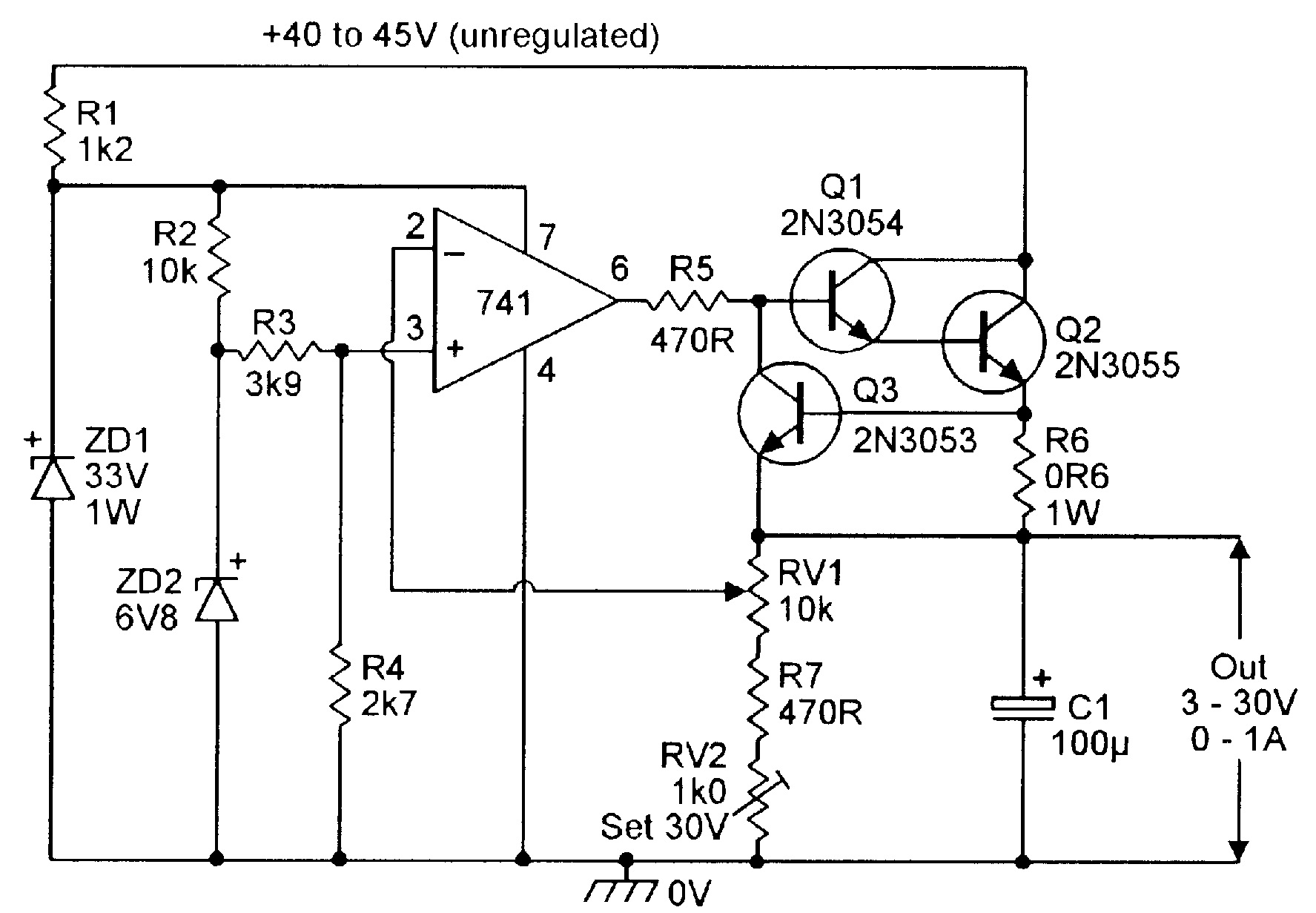
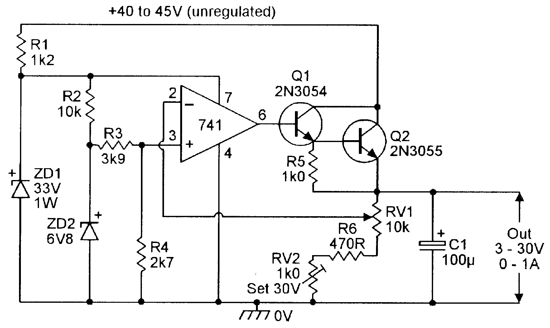 |
| FIGURE 21. 3V to 30V, 0 to 1 amp stabilized PSU. |
Figure 21 shows how the above circuit can be modified to act as a 3V to 30V, 0 to 1A stabilized power supply unit (PSU). Here, the available output current is boosted by the Darlington-connected Q1-Q2 pair of transistors, the circuit gain is fully variable from unity to x10 via RV1, and the stability of the 3V reference input to the op-amp is enhanced by the ZD1 pre-regulator network.
 |
| FIGURE 22. 3V to 30V stabilized PSU with overload protection. |
Figure 22 shows how the above circuit can be further modified to incorporate automatic overload protection. Here, R6 senses the magnitude of the output current and when this exceeds 1A, the resulting volt drop starts to bias Q3 on, thereby shunting the base-drive current of Q1 and automatically limiting the circuits output current.
 |
| FIGURE 23. Simple center-tapped 0 to 30V PSU. |
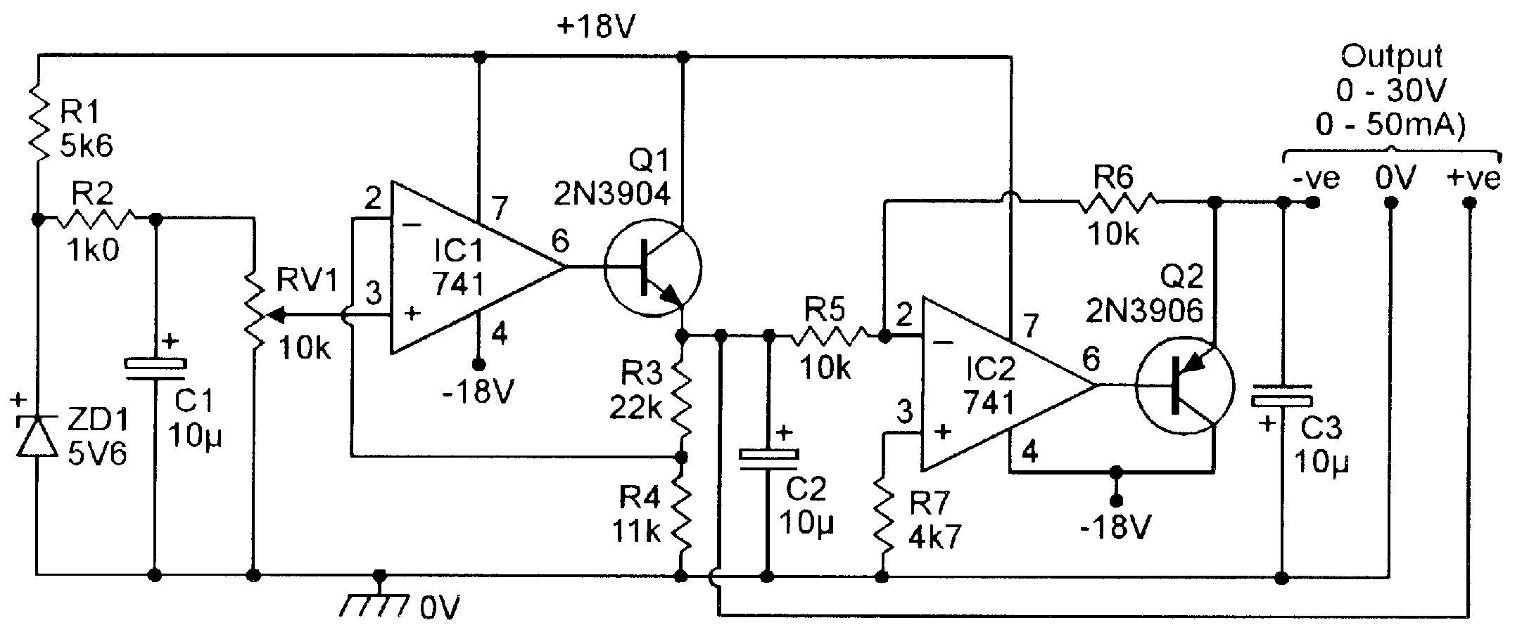
Finally, Figure 23 shows the circuit of a simple center-tapped 0 to 30V PSU that can provide maximum output currents of about 50mA. The PSU has three output terminals, and can provide either 0 to +15V between the common and +ve terminals and 0 to -15V between the common and -ve terminals, or 0 to 30V between the -ve and +ve terminals. The circuit operates as follows: ZD1 and R2-RV1 provide a regulated 0 to 5V potential to the input of IC1. IC1 and Q1 are wired as a x3 non-inverting amplifier, and thus generate a fully variable 0 to 15V on the +ve terminal of the PSU.
This voltage is also applied to the input of the IC2-Q2 circuit, which is wired as a unity-gain inverting amplifier and thus generates an output voltage of identical magnitude, but opposite polarity on the -ve terminal of the PSU.
The output current capability of each terminal is limited to about 50mA by the power ratings of Q1 and Q2, but can easily be increased by replacing these components with Darlington (Super-Alpha) power transistors of appropriate polarity. NV