Article Clarification
Some readers mentioned that the design procedure in my article, “An Elegant Approach to Design a Variable Voltage Divider” does not consider the load resistance effect on circuit operation.
The problem can be resolved by some extra calculations. Figure 1 shows an example with a 50K Ω load. As before, the load voltage has to change from +8 down to -5V.
The first step is to calculate RX and RY with no load. The second step is to convert the circuit to the left of the load into a Thevenin network. Figure 1-b shows the circuits when the wiper is at the upper end and at the lower end of RP. It’s easy to find that VMAX should be +8.660V and VMIN should be -5.513V.
The last step is to recalculate RX and RY for the new values of VMAX and VMIN. Figure 1-c displays the result.
Simulation shows the range of load voltages is slightly wider than what is required. The 1% deviation is completely acceptable.
Jordan Dimitrov
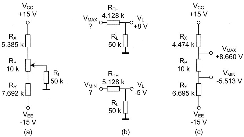
FIGURE 1. After you define RX and RY for the unloaded circuit (a), connect the load and get the Thevenin networks for the two end positions of the wiper (b), and recalculate RX and RY (c).
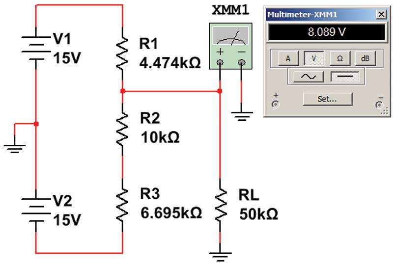
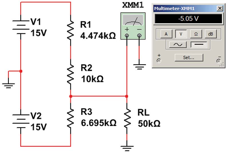
FIGURE 2. Load voltages for the two end points of the wiper.
Solutions Really Add Up
The N&V 2019 Issue-2 has an article called “Circuit Simulation Made Easy” that is excellent.
As a person who almost 50 years ago studied EE and who has forgotten much of the associated mathematics, I was floored by the simple solutions to circuit modeling that this article described.
I was so impressed I had to send this message to thank the author, C.A. Hamilton, for giving me the tool I needed for many of my projects.
Please pass on my thanks to Mr. Hamilton for his great article.
Frank Chiechi