Enjoy SMD capabilities using the at-home procedure outlined here.
A Surface-Mount Overview
Every day seems to offer new Surface-Mount Devices (SMDs) that tantalize you with a wealth of capabilities you can't find in through-hole components. In fact, many types of through-holes are getting harder to find as time goes by because Surface-Mount Technology (SMT) is a more profitable process for large manufacturers. SMT gives them higher device capability and it's streamlined to fit right into automated assembly. Device manufacturers are following the money. Although it looks like some through-holes will always be around, most are disappearing. There just isn't enough business in through-hole parts to justify making most of them anymore.
Because the length of the traces are shorter on SMT devices, they offer a real advantage in high-frequency applications. You also get more function on any given piece of real estate, which probably drives surface-mount technology more than anything else.
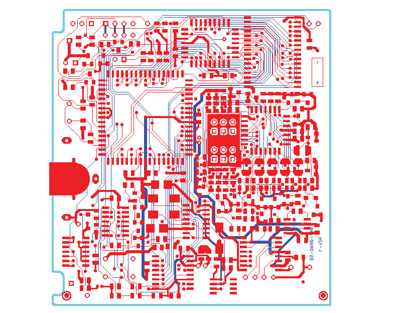
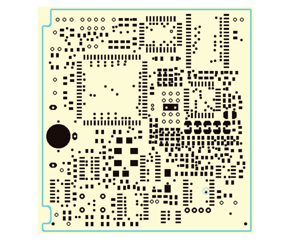
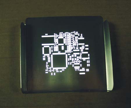
Basically, what you can build with surface-mount goes far beyond what you can build with through-hole as the SMT diagram illustrates (see below).
Still, purely surface-mount may never be a reality because even digital boards have connectors to plug them into the world. Connectors produce exceptional stress on the solder joints, which is a negative for SMT. Compared to through-hole, SMDs are easier to rip off the board. So, until somebody fixes this problem, components, like connectors, will continue to rely on basic through-hole technology. In the plant, this means they wind up reflow soldering the SMDs, and use wave or selective soldering for connectors and some analog devices.
The larger size of solder joints and wide spacing between leads on through-hole boards are easy to handle for anyone familiar with hand soldering. Soldering the tighter pitch on surface-mount devices is the main problem for a home workshop.
In defense of SMDs, printed circuit boards (PCBs) have glass fibers in them arranged in an X-Y direction, not in the Z direction. The coefficient of thermal expansion in X-Y is much less than it is in Z. So, whenever you touch a solder iron to the board, it expands more rapidly in the Z direction, causing stress in the barrels of plated through-hole and via. This stress can crack the copper barrel where it joins the pad on the board surface. SMD boards are more reliable in this area than through-hole boards.
Home Workshops and SMD Assembly Problems
So, you'd like to take advantage of some of the newer SMD capabilities, but may have avoided it because of the problems associated with hand soldering the leads. To compensate, many of you will have mixed technology boards built to your design spec, and then send them out to be assembled at a contract shop. This can add a lot of time and expense to your project unless you're really lucky and have a buddy or a long-standing relationship with a local shop that will put your one or two boards at the top of their production schedule.
You know that screen printing your solder paste and reflowing your assembly is the method you would choose if you could. Unfortunately, nobody has a screen printer or reflow oven that would even fit on your workbench — let alone be affordable.
Well, guess what? Now you can have both. The following method I'm going to take you through is far from the sophistication of major screen printing and reflow equipment, but it gets the job done — even double-sided SMT boards. You can do it right in your garage or workshop. It's possible to actually cut your assembly time, increase the quality of your designs, and open the door to all the mixed technology you want to experiment with.
I'll take you through all the steps using a prototype stencil tool developed specifically for your home shop and (don't laugh) a common toaster oven. Face it, building SMT boards at home will never be a “piece of cake,” but this new procedure should help make it a lot easier, and maybe save a little time and money by keeping more of your project in-house. Here's what we’ll be working with:
Material:
Solder Paste
Reflow Temperature Indicator
SMT Components
Printed Wiring Board
Equipment:
Prototype Stencil
Squeegee
SMT Placement Tools
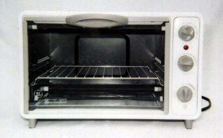
Toaster Oven
A vendor that I use to build my PCBs is PCBExpress. Regardless of what vendor you select, all tools in home stencil kits basically work in the same way. There are only so many low-cost ways to screen print at home — and, a toaster oven is a toaster oven. Most sources have at least two levels of kits available. What you want depends on how "single source" you like to be. Of course, all kits offer complete "How-To" instructions.
Ordering Your PCB and Prototype Stencil
First, you need to get your prototype stencil made. Although they're not just for prototype products, I like to call these stencils "prototype" to differentiate them from standard framed production stencils. These "frameless" type of stencils run from 50 percent to almost 85 percent less than the cost of conventional stencils.
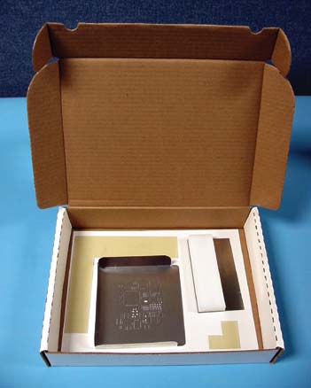
A basic prototype stencil kit comes with a prototype stencil, qqueegee blade, and PCB holder.
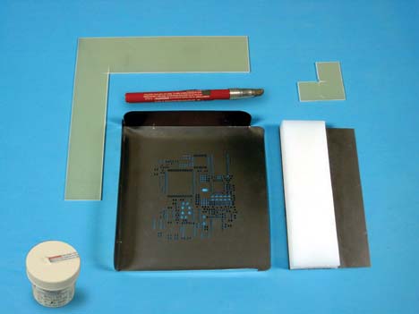
A starter prototype stencil kit also has solder paste and reflow temperature indicator.
You can have your board and stencil made by a single vendor as I did, or, if you already have your boards, there are vendors that will just make stencils. In the past, I've purchased prototype stencils for existing boards from Stencils Unlimited on the Internet (www.stencilsunlimited.com), and I'm sure there are others you can find with a simple web search.
To order a stencil, you need to send the vendor your Gerber files, just as you always do to get your design made up, but in a little different way, if possible. When you send in your board design, indicate both the silk screen and solder paste layer in your Gerber files. The PCB vendor will take those files and create the prototype stencil pattern from them.
Some of you may not have a software program that can create the silk screen and stencil layer files. In this case, the vendor can use the top and bottom copper Gerber files and edit them to create the pad openings in the prototype stencil that match your board design. It's a little more involved, but a common practice — even in a professionally run production. The big electronic contract shops run into this all the time, so don't fret if you don't have the capability to create these special files. Any good PCB or frameless stencil vendor does.
Choosing Your "Reflow" Oven
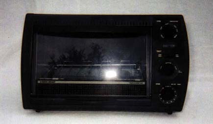
The only part of this project that you can't get from any PCB vendor that I know of, is the "reflow oven." The following toaster ovens have been tested and were found to meet the reflow requirements for most SMT PCBs — 9 x 11 inches or smaller. I can't guarantee the results you may get using any other models. This is a good size selection, and you can find most models well under $100 at any local discount store.
| Brand |
Model |
| GE |
106632 |
| Black & Decker |
TRO5900CT |
| Black & Decker |
TRO6100CT |
| Oster |
6230 |
| Oster |
6232 |
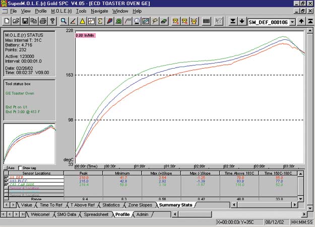
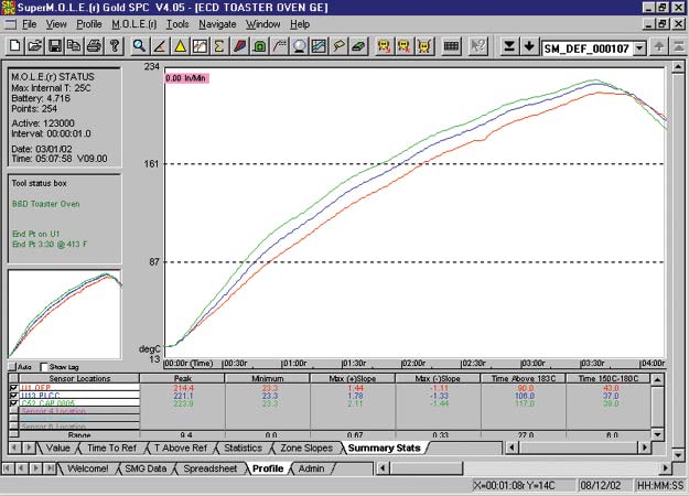
GE OVEN WITH SOLDER PROFILE
BLACK & DECKER TRO 5900TC WITH SOLDER PROFILE

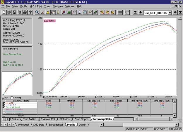
OSTER 6230 & 6232 WITH SOLDER PROFILE
These test results show the ovens and their associated thermal reflow profiles. You can see how close they are in capability.
Considerations Regarding Solder Paste and Components
Solder Paste: There are lots of solder paste manufacturers. Some don't provide printable paste in containers less than 500 grams. For a small number of PCBs, this would be expensive. What you want is standard eutectic tin/lead solder. This is typically available in either small jars or in the syringes that are used in rework stations. Most vendors providing home prototype stencils will have small jars of solder paste available, like the one shown here.
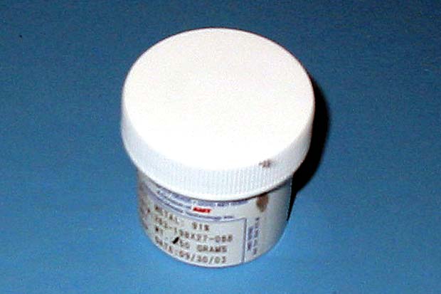
Be sure to check on this. Solder paste in small quantities costs around $0.25 to $0.50 per gram.
Paste for rework typically comes in 100 grams syringe sizes, but also has a lower percent of metal so the paste will flow through the syringe easier. Repair paste may slump on fine pitch components causing solder shorts. On QFPs, you may have to clear solder shorts with a fine-tip solder iron. Because of this, some manufacturers do not recommend using this type of paste for screen printing applications. But it's your choice.
A Few Cautions
Solder Paste: Most standard solder paste is shipped in a cold pack. It has a longer shelf life if refrigerated. Before using the solder paste, remove it from refrigeration and let it warm to room temperature (do not store solder paste in the refrigerator where you have food). If you don't have a safe place to refrigerate the solder paste, store it in a cool, dry place. Some prototype stencil vendors and solder paste vendors can provide a type of solder paste that does not require refrigeration, so again, be sure to check on this.
Solder paste contains lead. You have to dispose of unused solder paste and rags with solder paste on them as hazardous material. Talk to your solder paste supplier about taking this hazardous material back for recycling. If the solder paste supplier won't take this material back, he can usually tell you how to dispose of it safely.
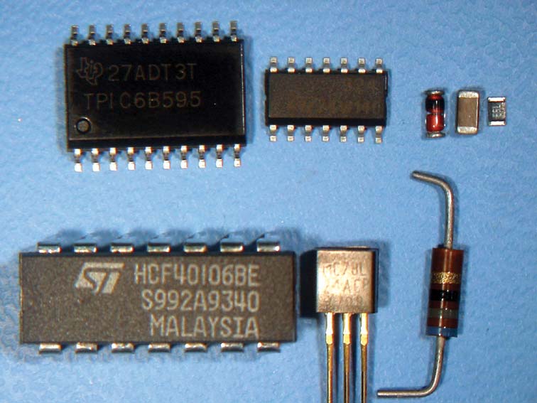
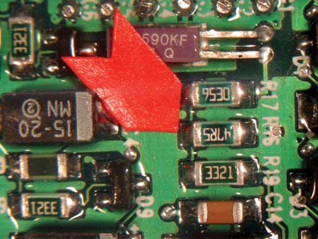
Components: There are far too many types of SMDs to go into here. Suffice it to say, if you want it done, there is a device for any application you can think of. Ask your component manufacturer or supplier.
All SMD component manufacturers provide the solder process thermal requirements for the components they produce. Always request this and control the oven profile to conform to this data.
Some SMT components have restricted thermal process requirements. Be sure to verify that all components can be processed using a standard SMT procedure, as described here, before you buy them.
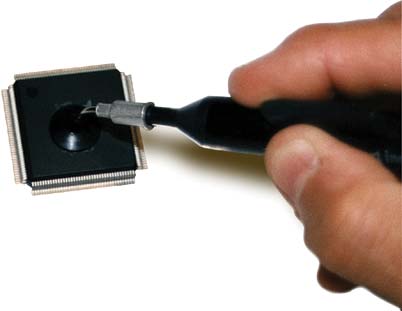
The leads on all SMDs are delicate — some more than others. The finer the pitch, the easier to damage the leads. Handle as little as possible, and if applicable, keep in their holders until ready for placement. It's best to use a vacuum wand to place very fine pitch devices.
Building Your Board
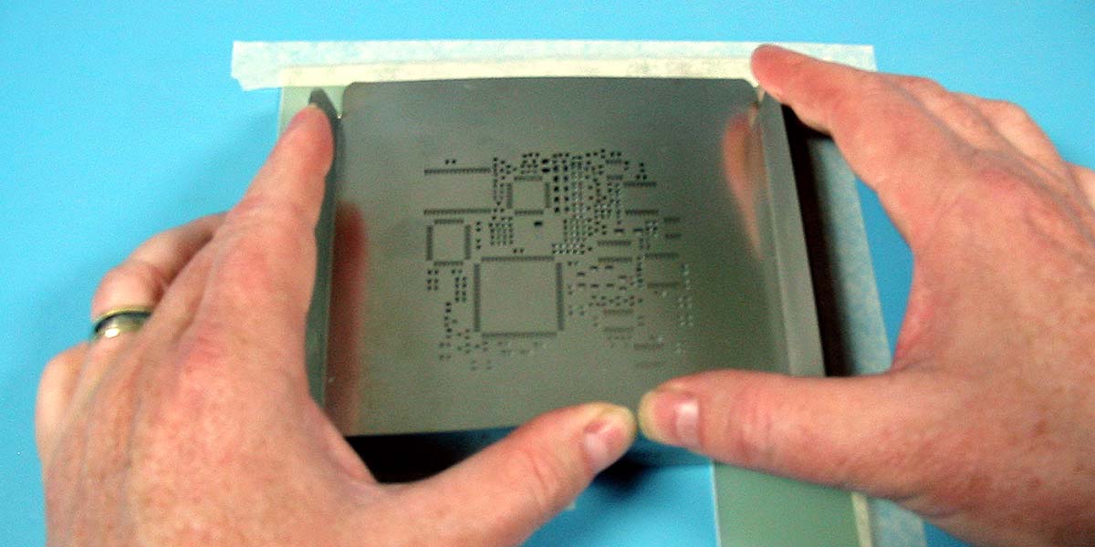
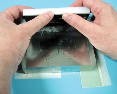
1. Set up your prototype stencil. Important: All work surfaces should be conductive and grounded.
Prototype Stencil: The prototype stencil is a stainless steel foil (five to 10 mils thick) with openings cut through to allow the solder paste to be deposited onto the PCB lands (pads). To prevent the PCB from moving, you can tape it down or make a smaller square and use it as indicated.
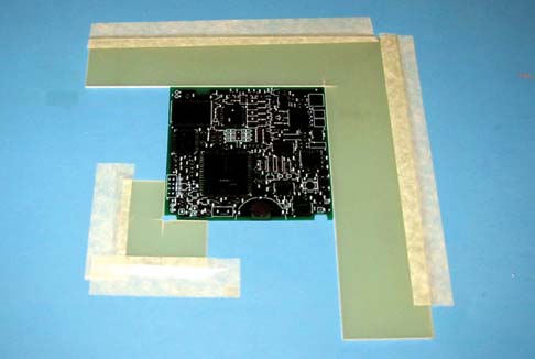
- Place the large L-shaped board holder on a flat surface and tape it down to prevent it from moving.
- Place the PCB into the board holder.
- Place the small L-shaped board holder next to the PCB and tape it down to prevent it from moving.
- Align the prototype stencil over the PCB SMT land pattern (SMT pads) and tape it to the large L-shaped board holder.
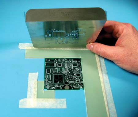
2. Apply the solder paste using your prototype stencil.
Remember: If using refrigerated solder paste, be sure to remove it from refrigeration and let it warm to room temperature. Before printing with solder paste provided in a jar, stir it for five minutes. Do NOT store paste that is not delivered in a cold pack in a refrigerator.
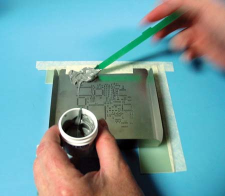
Place the solder paste on the prototype stencil to one side of the hole pattern. Spread the solder paste the full width of the hole pattern.
Squeegee: The squeegee is a flexible blade of stainless steel used to roll the solder paste over the prototype stencil, forcing the solder paste through the prototype stencil and onto the PCB lands.
While holding the prototype stencil in contact with the PCB, take the squeegee and place it on the prototype stencil outside the solder paste. Tilt it 15 to 20 degrees from the vertical (toward the solder paste), and drag it and the solder paste across the hole pattern.
Hold a light to medium pressure on the squeegee against the prototype stencil. Carefully lift the prototype stencil away (UP) from the PCB. You may have to experiment a little to find the best angle for the type of solder paste you're using.
Inspect the solder paste print to ensure all the lands have solder paste on them and the paste is not smeared. If the print is not good, immediately use a spatula to remove the solder paste from the PCB. Clean the paste that remains on the PCB with alcohol and a clean rag. Let the PCB dry and print the solder paste again.
3. Place components.
Important: Keep the time between printing the solder paste and placing the SMT parts on the solder paste short. The paste manufacturer can guide you on the maximum time between printing and placement.
Place the SMT parts on the PCB using tweezers or a handheld vacuum placement tool. (Use a magnifying glass, if needed, to align fine pitch leads to the land pattern.)
4. Using reflow temperature indicators.
There are two reasons to use a temperature indicator. First, to create good solder joints, solder paste has to reflow, or melt, at a certain temperature and stay at that temperature (liquidous) for a given amount of time. When you buy your paste, this information is provided by the solder vendor. Next, your SMDs are temperature-sensitive, so you want to know how long they can be exposed to the reflow or melt temperature without damage. A temperature indicator is designed to tell you this by the way it reacts within the oven.
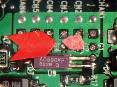
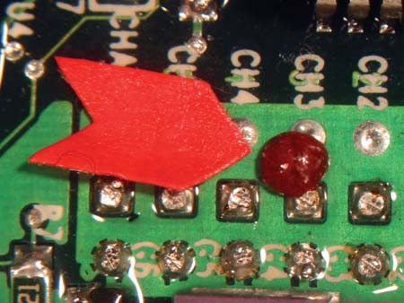
There are several types, but the one I use looks like a big crayon. I use this to make a mark on the board.
Some of these are hard to mark with, so I often just shave off a tiny bit of flakes onto the board with a knife tip. You might want to slice a small piece off. Either way works fine. It melts at the specified temperature.

Different temperature indicators have different colors. For this process, the indicator marks are light in color. They look a little like dust on the board — almost like flakes of talcum powder. When they melt, they slump and change color. This particular one goes from light pink in color to a clear red, so it's easy to see. Obviously, it has to be near the window of the toaster oven where you can readily see the change.
5. Reflow your assembly in the toaster oven.
Important: Before reflowing starts, turn the oven on to heat up — a minimum of five minutes. Set the oven to bake and set the temperature to the highest baking temperature setting (450 to 500°F).

Before placing the PCB in the oven, mark it on the top side next to the edge that will be nearest to the oven door, with the reflow temperature indicator (413°F).
Make sure that you can see the temperature-stick mark through the oven door. If the edge of the board has a breakaway, do not mark the breakaway, mark the edge of the PCB. If there is not a clear area on the edge of the PCB, mark the interior of the PCB next to a large component (PLCC or QFP) with the reflow temperature indicator.
NOTE: The edges and corners of the PCB will be hotter than the interior of the PCB. If the temperature marker is used on the interior of the PCB, the corners and edges may get too hot and damage the board or the SMT components.
When the temperature-indication mark melts, remove the board from the oven. Be careful not to disturb the molten solder joints. Place the board on a surface and let it cool until near room temperature. Inspect the solder joints using your solder joint inspection criteria or the IPC 610 requirements.
Temperature marker before reflow.
Temperature marker after reflow.
If you have more than one board, place the next PCB in the oven after marking the board with the temperature stick. If any of the solder joints on the first board did not reflow properly, mark the PCB next to the location that did not reflow with the temperature indicator (413°F). Use this location to control the reflow length for the subsequent boards, or to redo the reflow process on the original board.
A flashlight can help when watching the temperature indicator material change in form. When using a toaster oven, this visual method is the only reliable reflow guide. You have to watch the material to judge reflow time. Every board is different, so time is not a good control (one minute, five minutes, 20 minutes, etc.). There just isn't any "average reflow time" for these types of projects. To suggest any would only confuse the issue and could actually hurt, rather than help, your project.
Remove the PCB after the temperature-stick mark melts, let it cool, and inspect the solder joints. Repeat the above steps until all your PCBs are reflowed. Turn oven off.
6. Screening a double-sided board, side two.
After populating and reflowing the side with the smallest components, repeat the process on the side with the larger SMT parts. This sequence will keep the largest and heaviest parts from hanging upside down during reflow, reducing the likelihood that they would fall off. Molten solder has very high surface energy, and can hold most SMT parts, even upside down.
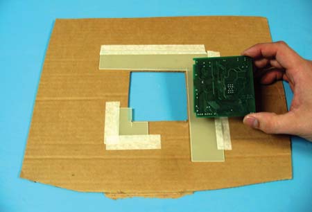
Print the second side with the PCB on cardboard (cardboard is the easiest, but you can use wood or any non-static generator) that is large enough to attach the L-shaped board holder and your board assembly. Use cardboard that is thicker than the populated PCB and thick enough to function as a support for the screening process.
The cardboard should be cut out to clear the SMT components from the first reflow. Again, make sure all work surfaces are ESD safe or grounded.
7. Reflowing side two.
When you reflow the second side of the PCB, the whole assembly has to be held off of the oven shelf with standoffs. You'll damage the SMT solder joints from the first reflow if you lay the board directly on the oven shelf.
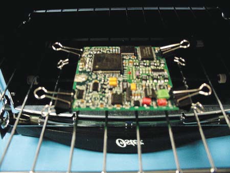
You can use any material that can withstand the oven temperature to create standoffs to hold the board, but the very best is scrap FR4 material. You probably have some old board scraps laying around, but if not, just prop the assembly up on a couple of pieces of metal, or anything that is not going to be affected by the heat of the oven. I used large binder clips for this board and they worked fine.
8. Touching up defective solder joints.
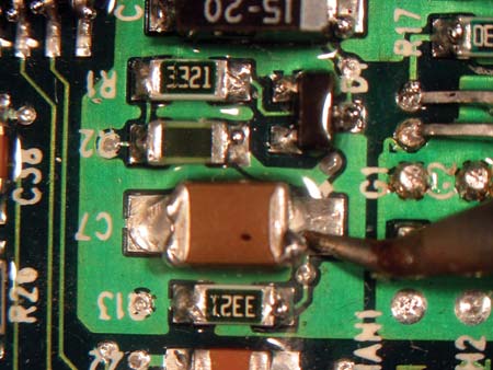
Touch up any solder defects with a solder iron. Use a fine tip on the solder iron and don't let the tip touch the body of the SMT parts. Set your solder iron temperature as low as possible. A solder iron that is set to a high temperature can thermal shock SMT components.
That's it! You now have your finished boards, ready to test and use in your latest project.
Make sure you handle your SMT and mixed technology SMD board(s) carefully. They're not as rugged as 100 percent through-hole, but what you can create with them is far beyond anything you could ever get with only through-hole.
Experiment. Have fun. NV
Cautions and Handy Information
Warning: Using Common Sense
- Solder paste contains lead. Do not eat or drink around solder paste.
- Do not use a toaster oven to prepare foods after it has been used for solder paste reflow.
- Wash hands after working with solder.
- Ovens are hot — use insulated gloves and safety glasses while working around hot equipment.
- Some SMT components have restricted thermal process requirements. Verify that all components can be processed using a standard SMT process as described in this procedure.
- Do not store cold pack solder paste in a refrigerator used for food, and never store room temperature solder jars in a refrigerator.
Solder Paste Shopping Guide
If you have questions about paste, you want to talk to a reliable source — usually someone other than a distributor. Solder paste manufacturers will always answer your questions and you can easily find them on the Internet (search on "solder paste"). You can sometimes purchase small quantities directly from some manufacturers. A better bet might be smaller distributors or you can purchase solder paste as an option in many prototype stencil kits.
Here are a few well-known paste manufacturers in alphabetical, not priority order, and definitely not the only sources around. This is just a sample for your information:
AIM
Amtech
Cobar
EFD
ESP
Heraeus, Inc.
Indium Corporation of America
Kester Solder
Multicore
OMG
Qualitek International, Inc.
Senju
Learn How to Recognize a Good Solder Joint
I'm sure that many of you are either associated with, or at least aware of, the Institute for Interconnecting and Packaging Electronic Circuits (IPC). This is the best source I can point you to regarding all the guidelines you need to build and inspect a product-worthy board assembly. The documents below are extremely helpful, even if you're an old pro. You can order them — and much more — directly from IPC at the address below.
• IPC 610 is an industry SMT solder joint quality standard
• IPC/EIA J-STD-001C: Requirements for Soldered Electrical and Electronic Assemblies
• IPC-D-279 Design Guidelines for Reliable Surface Mount Technology Printed Board Assemblies
IPC
www.ipc.org