Here’s a simple circuit I came up with as part of another project I was working on to measure the acceleration of a model rocket in flight. While my original data storage requirements for that project were very specific (and very basic), I realized that the datalogging circuit and code had many other uses. This datalogger is suitable for just about any application where a small, cheap, low power circuit is needed to sample analog voltages, convert them to digital values, and store a modest amount of data in non-volatile memory.
The circuit shown in Figure 1 is based on a Microchip PIC16F876A microcontroller. This chip has a built-in five-channel 10-bit analog-to-digital converter (ADC), but only four channels are shown being used. It’s very simple to modify the code to use from one to all five ADC channels (more on this later).
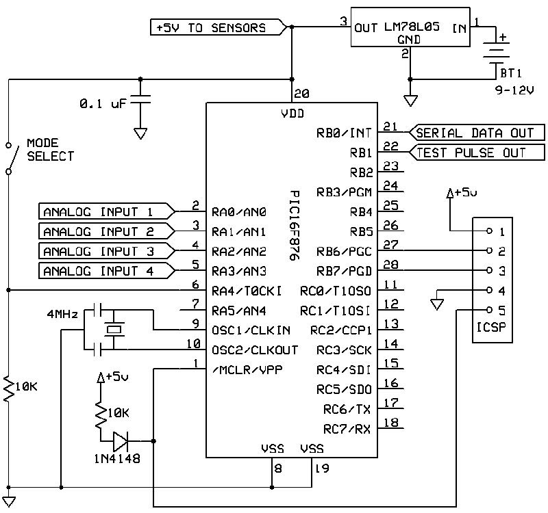
FIGURE 1. Four channel datalogger schematic.
(As a side note, Microchip doesn’t necessarily recommend the PIC16F876A for new designs. However, it’s still sold by many companies. Microchip suggests the PIC16F18877 as a replacement.)
A linear voltage regulator (such as the LM78L05) powers the PIC and any five volt tolerant sensors which may be added to the circuit. One mode-select jumper is used to place the microcontroller in data acquisition mode or in “data dump” mode.
An in-circuit serial programming (ICSP) header is included to reprogram the PIC after the circuit has been assembled, along with a diode to prevent the programming voltage from getting into the rest of the circuit via the five volt bus.
The PIC16F876A contains three different types of memory: 368 bytes of RAM; 256 bytes of EEPROM; and 8,192 words of Flash program memory. There isn’t enough RAM or EEPROM for serious data storage, and the Flash memory is for the program code, so where can our data go?
Well, if we’re very careful, we can use the WRITECODE and READCODE instructions in PICBASIC PRO (available at [url=http://www.melabs.com]http://www.melabs.com[/url]) to store that data in the Flash program memory. The code listing (available with the article downloads) only uses about 400 words of program memory. That leaves nearly 7,800 words for data storage; enough to capture more than 1,900 samples of the four 10-bit ADC values.
The code starts out by defining variables; the most important of these is the “pointer” variable. This defines the address in the Flash memory at which the data will be written during data acquisition. The initial value of this variable is set at an address beyond the last word of program code, so there is a bit of unused memory between code and data.
If you modify and recompile the code, you must check how many words your new code occupies and adjust the initial pointer value accordingly to make sure your data can’t overwrite your code.
Next, the code checks the status of the mode select jumper on pin RA4 and jumps to either the data acquisition loop or the data dump loop. The two loops are very similar in structure, using the same variables to cycle through the ADC channels and either write to or read from the Flash memory.
Each loop is terminated with an END command, so that when all of the memory has been written or read, the PIC will enter a power-saving sleep mode.
The number of ADC channels used is determined by the “channel” variable, which is used to set
the number of times the ADCIN command is executed in each pass through the data acquisition loop. As mentioned earlier, the maximum value for this variable can be anywhere from 1 to 5.
A datalogger isn’t much good without some sort of time reference associated with your data. The code provides a relative time stamp for each set of data through a pause command, which is calibrated to provide the desired delay between data acquisitions. This calibration is accomplished using the “test pulse out” signal on pin RB1 and an external frequency counter.
The code as written will collect data every 0.1 seconds using a pause value of 94 milliseconds, as near as my frequency counter could resolve. A pause value of 994 milliseconds should give a one second interval between data acquisitions, and so on. Remember to recalibrate this pause interval whenever you make changes to the code in the data acquisition loop.
Once your datalogger is full, power it down and connect it to a standard serial (not USB) port. (We’re talkin’ old school here.) Only the receive data and signal ground pins on the computer’s serial port need to be connected.
The computer should be running a terminal emulation program set at 2400 baud, no parity, eight data bits, and one stop bit (2400 N81). Also, make sure that the software is not set to use hardware handshaking. It’s a bit slow downloading this way — taking a minute or two to dump the whole memory — but this makes it very tolerant of different circuit construction techniques and unshielded data cables.
Before powering up the datalogger, you must install the mode select jumper so the program will begin downloading the data. If you don’t, the PIC will begin collecting more data and overwriting whatever was there before.
The data dump loop formats the data into separate lines for each time reference, with the values in each line separated by commas, starting with the first ADC channel. The data can then be easily imported into a spreadsheet in a comma-separated variable (CSV) format and processed or graphed as needed. Depending on the exact number of data sets recorded, the last line of data may contain some invalid values that will need to be ignored.
Application: Rocket Accelerometer
My rocket-borne implementation of this circuit is shown in Figure 2.
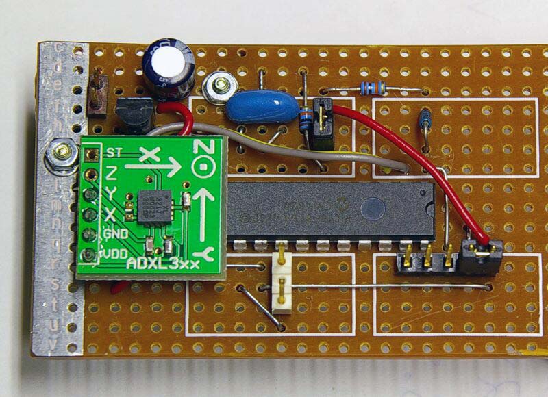
FIGURE 2. Rocket datalogger circuit with two-axis accelerometer daughterboard.
I’m using an Analog Devices’ ADXL321 two-axis evaluation board to measure the acceleration over the rocket’s flight profile. Note the five-pin connection for ICSP, the mode select jumper, and the serial data output connector (the one with the white base).
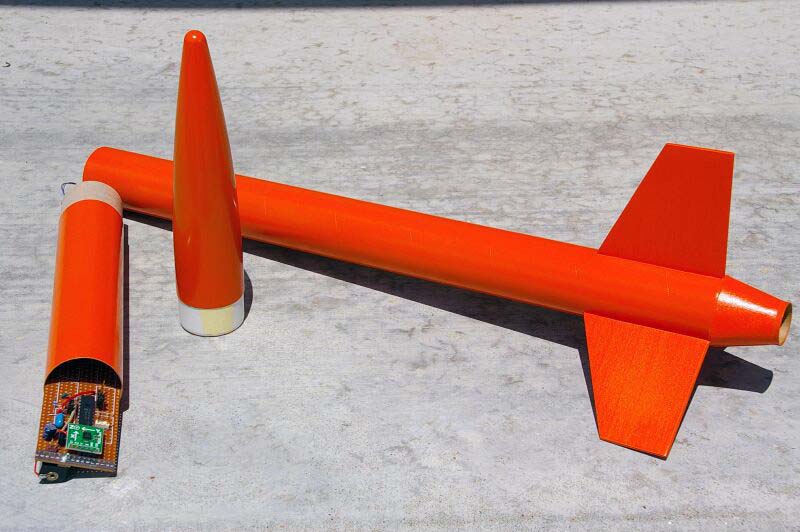
FIGURE 3. The datalogger fits neatly inside my launch vehicle.
A 12V A23 battery in an N-cell holder is bolted to the back of the board, and an additional two-pin jumper is used as an on-off switch.
The circuit layout is non-critical, but all components must be firmly soldered, glued, or otherwise held in place to endure the stress of launch (the ADXL321 has a range of ±18 G, to give you an idea of what I’ve built it to endure). There are three ADC channels and plenty of board space left for additional sensors.
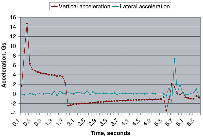
FIGURE 4. Plot of the captured acceleration data during launch and landing.
Have fun keeping track of your world with this datalogger — now there’s no excuse for not knowing what’s going on! NV
Parts List
PIC16F876A microcontroller
4 MHz ceramic resonator with capacitors
LM78L05 five volt linear regulator in TO-92 case
(2) 10K ohm resistors
1N4148 diode
0.1 µF capacitor
(2) two-pin and (1) five-pin header
Downloads
Schematic, Code, Excel Spreadsheet file.