Design Concepts and Hardware Fabrication
The early days of electronic computers used teletype machines and line printers, and later, alphanumeric screens and keyboards as their primary input-output devices. As computer usage grew beyond census and accounting applications, the need for improved graphical displays and output devices became apparent.
Graphical display terminals using large screen cathode ray tubes (CRT) soon evolved. These displays were essentially “up-sized oscilloscopes” whose X-Y beam deflection was driven by a computer.
Figure 1 shows a specialized XY CRT terminal that was part of SAGE (Semi-Automatic Ground Environment): an early air defense system deployed in the US.
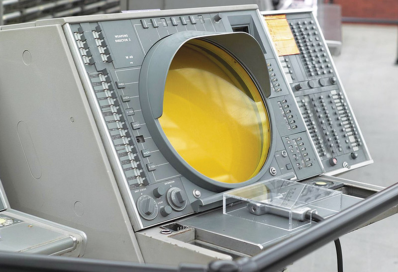
FIGURE 1. SAGE air defense system used an XY interactive graphics terminal.
By the late ‘70s, Tektronix, Hewlett-Packard, and others sold general-purpose XY graphics terminals able to show graphs, charts, and line drawings of all types.
While a far cry from what we take for granted today, these were important stepping-stones in the evolution of computer graphics and display technology.
Arduino Graphics Interface
As an undergrad electrical engineering student some eons ago, I worked on a MODCOMP (Modular Computer Systems, Inc.) 16-bit minicomputer that featured a large 19” Hewlett-Packard XY graphics display screen. A few months ago, I began to wonder: Would it be possible to replace those half dozen racks of circa 1975 minicomputer hardware with one of today’s $50 credit-card sized computers?
The answer proved to be YES! What resulted, I call the Arduino Graphics Interface, or AGI for short. With AGI, you can transform a leftover analog oscilloscope into a high resolution computer graphics display and gain valuable insights into computer graphics, digital-to-analog conversion (ADC), and advanced Direct Memory Access (DMA) hardware and software techniques. It’s easy to add a real time clock (RTC) module and interactive controls to turn the AGI platform into a “CRT CLOCK” (Figure 2) or other high resolution computer graphics display device.
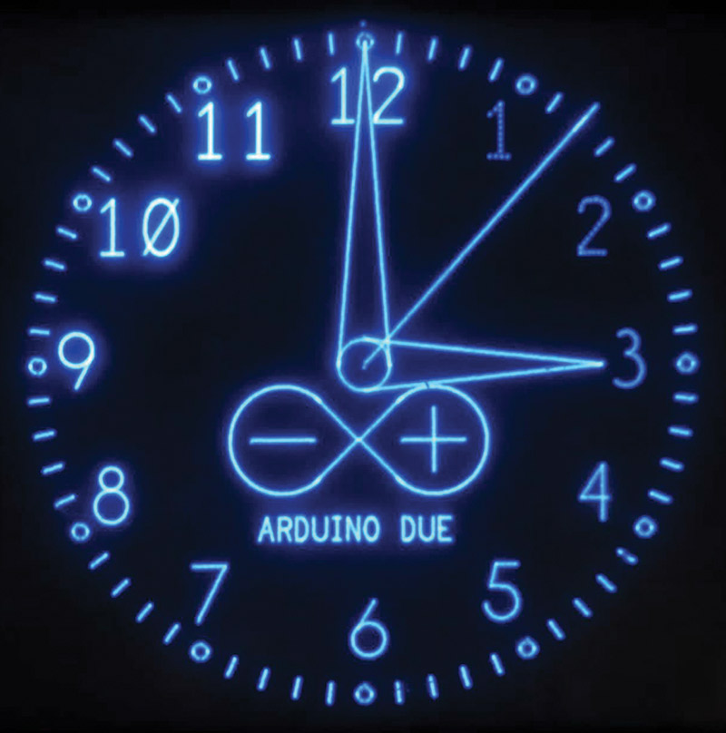
FIGURE 2. AGI can become a CRT CLOCK!
In this article, we’ll focus on the overall concepts, circuit design, and hardware fabrication. In Part 2, we’ll integrate the hardware to XYscope: the software control and plotting library that enables an Arduino Due CPU + analog oscilloscope to become a high resolution XY graphics display. Let’s get started!
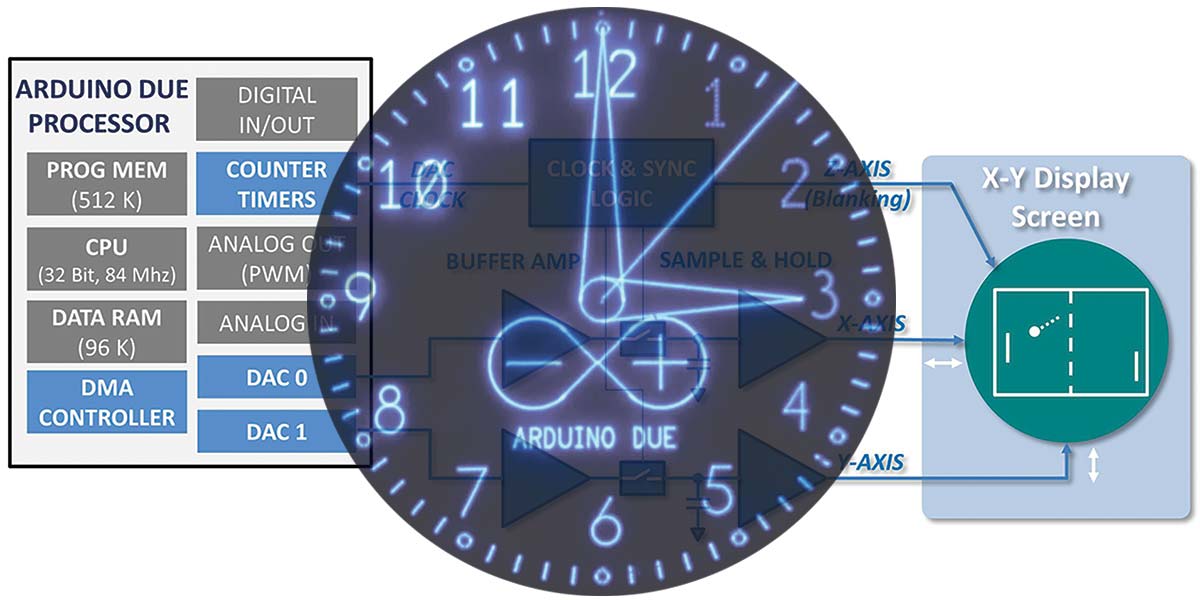
AGI Block Diagram & Operational Overview
The block diagram of the AGI is shown in Figure 3.
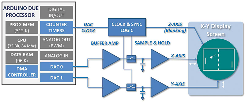
FIGURE 3. Arduino Graphics Interface block diagram.
You can see that a pair of digital-to-analog converters (DACs) inside of the ATMEL SAM 32-bit CPU (the heart of an Arduino Due) is used to drive the X and Y axes of an analog oscilloscope. Rather than use the normal oscilloscope Amplitude vs. Time display mode, we run the scope in X-Y mode. That is, the internal oscilloscope time base that usually drives the X axis is not used, but rather all XY information for deflecting the CRT beam comes directly from the Arduino through the AGI circuits.
To create graphical images with AGI, the programmer need only build a list of 12-bit X-Y integers that make up the individual points we want to show. One after the other, the DACs of the Due receive and convert each XY integer coordinate pair into small X-Y voltages that drive the CRT beam about the oscilloscope screen. The block diagram shows that we also provide a blanking pulse (a.k.a., Z axis blanking) as a third signal to the scope.
As with all CRT type displays, one must repeatedly send the whole display list to the screen to keep the points visible and refreshed. Even though the points are actually flashing at a very high rate, human Persistence Of Vision (POV) causes the displayed image to appear stable and flicker-free.
Key AGI Features
High Resolution — By using 12-bit DACs, we have a display resolution of 4096 x 4096. This exceeds even HD TVs and beautifully renders smoth step-free lines, arcs, and characters.
Easy to Use — To display graphical images, the AGI programmer simply creates a list of XY integers to define the individual points to be plotted. A small background process automatically sends the point-list to the CRT.
Ready to Use — A graphics and control library of simple subroutine calls makes it easy to create and load graphic and alphanumeric content into the XY point-buffer. The AGI Library includes:
- Plot POINT, LINE, RECTANGLE, CIRCLE, ELLIPSE, CIRCLE-ARC-SEGMENT, ELLIPSE-ARC-SEGMENT
- Plot CHARACTER, TEXT_STRINGS, INTEGER NUMBERS, FLOATING POINT NUMBERS
Complex Graphics Possible — The display list can contain up to 15,000 X-Y points so that complex objects can be rendered.
Fast — The Due is a very fast processor that can very quickly calculate and store points into the XY display list array. There’s plenty of processor time available to make changes in the list, making animated graphics easy.
Educational — The AGI is a great introduction to graphical coordinate systems, X-Y point/vector style computer graphics, and DACs.
AGI is also a solid demonstration platform to learn and utilize counter-timers and DMA technology.
While It’s Pretty Cool, there are Some Limitations
The AGI uses an analog oscilloscope for its graphics output display. You’ll have to dust off your old analog oscilloscope or perhaps buy a vintage unit off eBay. The Oscilloscope Requirements sidebar details the features you need to look for when evaluating possible scope candidates for use with this project. Since we use an oscilloscope as the display screen, the size and display color is fixed by the cathode ray tube inside the scope.
While each individual point is displayed on the screen as either ‘full ON’ or ‘full OFF,’ variable brightness is easily achieved by varying the point-density of the dots that make up each graphic feature (more on this in Part 2).
Why an Arduino Due?
At first, I labored over the multitude of CPU boards available, but it soon became apparent only one board would “Due.” (I know, it’s a terrible pun.) Even though the Beagle Bone and Raspberry Pi families have faster CPUs and more memory, only the Arduino Due CPU includes a pair of DMA-driven on-chip DACs.
Getting XY Data Out to the Scope
While programmed I/O using an Arduino analogWrite() command is a common way to output data to the DACs, the AGI uses DMA techniques. We’ll discuss this further in Part 2, but for now, suffice it to say that we connect the DMA hardware inside the Due to a COUNTER-TIMER which automatically sends the X-Y data array out through the DACs to the oscilloscope screen at very high speeds.
DAC Performance
For the AGI project, the Due provides two DAC outputs; each of which translates a 12-bit unsigned integer into one of 4,096 different analog voltage levels. As measured at the processor DAC pins, the CPU outputs a voltage of 0.5V when converting the integer value 0, and outputs 2.75V when converting the integer value 4095. Dividing this 2.25 volt peak-to-peak voltage range by 4096 means that each step or bit change at the DAC input results in a 550 μV change at the DAC output. These signals are buffered by the AGI circuits before they are sent on to the oscilloscope for display.
In addition to resolution, DAC speed is also important. Speed is defined as the time it takes for the DAC to change its output voltage in response to a change at its digital input. A perfect DAC would have zero conversion time, but reality falls short. The rise times, fall times, and settling times of the DACs are important to the AGI project as they define the rate that can be used to send points to the scope screen; this, in turn, sets the maximum number of points we can display within our target POV window of 20 ms.
Since DAC speed is not specified in the ATMEL SAM datasheet, I wrote a small AGI program to drive the DACs from 0 to 4095 and then back to 0, so that I could make my own “worst case” full-scale speed measurements.
Using an oscilloscope to monitor the DAC outputs, Figure 4 shows that a full-scale change in output of the DAC from 0 to 4095 in one step takes slightly over 300 ns. Similarly, the step going from 4095 back to 0 is seen to be about 300 ns as well.
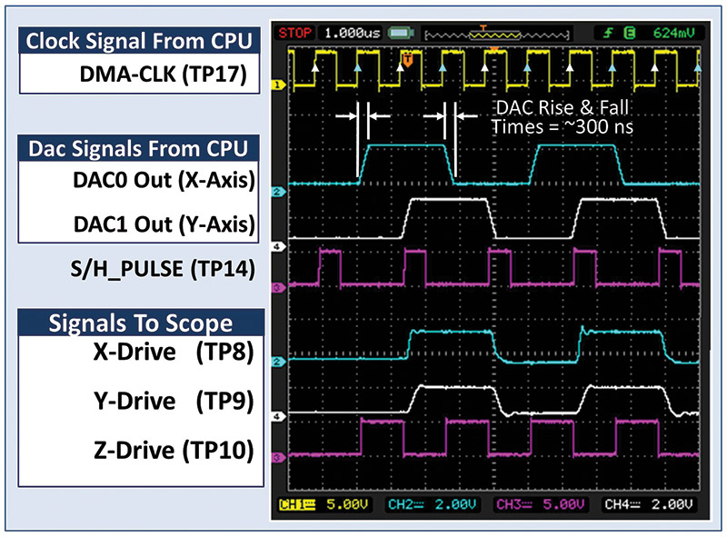
FIGURE 4. DAC speed and AGI timing signals.
Figure 4 also shows a few other aspects of the overall timing. First off, observe that the DMA_CLK (TP17) signal (one of the Due Counter-Timers) drives the rate of the DMA transfers and therefore the pace of digital-to-analog conversions.
Next, note that the X and Y conversions follow each other in time, with the DAC0 signal (the X axis value) changing first, followed one DMA_CLK cycle later by the DAC1 signal (Y axis). Analog sample and hold circuits are used to time-synchronize the X and Y signals to one another before they are sent out to the oscilloscope as the X-Drive (TP8) and Y-Drive (TP9) signals for display.
Finally, the Z axis signal Z-Drive (TP10) is used to turn the CRT Spot on (logic 1 = “unblank”) every time a new point pair is ready for display on the screen. The CRT Spot is then turned off (logic 0 = “blanked”) just before the X-Y signals are “moved” to the next point to be plotted. Blanking the beam in this way keeps the display crisp and free of DAC settling times and other point-to-point transition artifacts.
Given the DAC rise and fall times, it’s possible to determine the highest DMA_CLK frequency we can use. My tests show reliable high quality graphics plotting can be achieved at DMA_CLK frequencies up to 800 kHz. Above 800 kHz, the DAC rise and fall time delays begin to distort the graphics display, appearing as incorrectly plotted points on the oscilloscope screen whenever adjacent members in the XY list are far away from one another.
Using a Timer to Trigger CRT Refresh
As noted, we need to repeat the DMA transfer over and over again to keep the CRT scope screen lit up. To do this, the AGI uses a second timer to create a “Time-to-Refresh” interrupt once every 20 ms. Every time we receive this interrupt, a new CRT screen-paint cycle is initiated. This repaints the screen 50 times per second, above discernable POV flicker rates.
With the DMA_CLK frequency set to 800 kHz, it’s possible to send about 10,000 points to the screen within the 20 ms target refresh interval. When more than 10K points are present in the display list, the software driver will automatically extend the refresh interval as needed so all points can be displayed. Depending on the phosphor decay characteristics of your oscilloscope screen and your personal POV sensitivity, you will probably notice the onset of image flicker when plotting more than about 12,000 points.
Circuit Details and Theory of Operation
The AGI schematic is shown shortly in Figures 7-9. I’ve included many test points (TPxx) in the design to facilitate testing and troubleshooting.
POWER SUPPLY — Any wall wart that can supply 12-15 VDC at .5 amps can be used to power the AGI circuitry. As shown in Figure 5, onboard linear regulators provide clean low-noise regulated +9.75V and +5.0V outputs to power both the AGI analog circuits (9.75V) as well as the logic and Arduino Due CPU (5.0V).
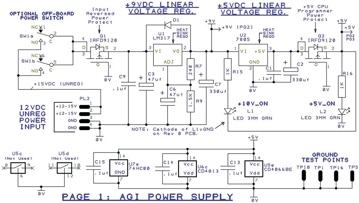
FIGURE 5. AGI power supply circuits.
Construction Note: Both voltage regulators U1 and U2 get warm and must be mounted to heatsinks. The two devices must use insulating hardware if they share a common heatsink or if either heatsink is grounded. Use large heatsinks to dissipate more heat if driving the AGI power input with more than about 12 VDC.
X-Y BUFFER AMPS — In Figure 6, you can see that the DAC0 (X axis) and DAC1 (Y axis) signals from the Due are received and buffered by high frequency op-amp U4. Potentiometers are provided at this stage so that signal gain (amplitude) and offset (screen position) for X and Y can be independently set. The gain pot on each output will vary the amplitude within a 1.0V to 4.0V P-P range. The centering pot varies the signal offset so that it can reside anywhere within a .2V to 4.75V window. Final display adjustment will be a combination of these AGI pots, as well as the oscilloscope gain and centering controls; my scope works well with AGI outputs adjusted to 1.5V P-P centered about +2.5 VDC.
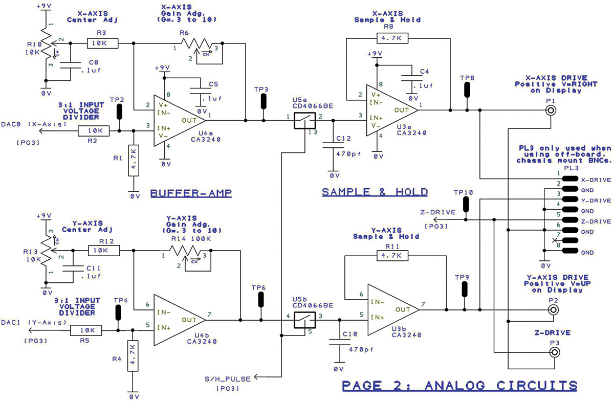
FIGURE 6. Analog section of AGI circuitry.
SAMPLE AND HOLD CIRCUITS — As seen in Figure 4, the DAC0 and DAC1 outputs are not simultaneously output by the Due CPU; the X value is converted first, followed by the Y value one DMA_CLK cycle later. Analog switch U5a-b, hold capacitors C9 and C13, and buffer amps U3a-b make up the pair of Sample and Hold (S/H) circuits that align and synchronize the X-Y point pair voltages, so they change together when they’re sent to the oscilloscope for display. The X and Y buffer amps are followed by transmission gates U5a-b and output op-amps U7a-b which work together to form two independent S/H circuits.
So, how do these S/H circuits work? Looking at the X axis path, it shows that whenever transmission gate U5a is turned on, the X axis voltage output of U4a is connected to C12 and buffer amp U3a. When U5a is turned off, C12 stores (a.k.a., “remembers”) the voltage, holding the X axis voltage stable even though the DAC output itself begins to change in response to the next conversion cycle.
U5b, C10, and U3b perform the same S/H function for the Y axis signal.
DATA CLOCK TIMING — COUNTER_TIMER_0 of the Due is programmed to be the DMA_CLK. This signal drives the internal DMA operations, but as shown in Figure 7, also comes to the outside world through CPU pin D2. This signal is fed to U6a and U8b to create all the needed AGI timing signals. Flip-flop U6a divides the DMA_CLK by 2 to create a signal that represents a point pair transfer completed signal or POINT_CLK. The POINT_CLK_NOT signal is then combined to generate the S/H_PULSE and the SHOW_POINT signals. As depicted in the timing traces of Figure 4, the S/H_PULSE signal is used to “grab and hold” the X-Y voltage pair. Then, the SHOW_POINT pulse is sent to the Z axis of the oscilloscope (a.k.a., “Z-Drive”) to unblank each point after it has settled down and is ready to be illuminated.
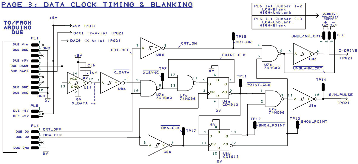
FIGURE 7. Timing and logic.
Build Note: Jumper PL6 is used to select the “blanking polarity” and is set to match the blanking logic used by our particular oscilloscope.
BLANKING SYNCHRONIZATION — It might seem a bit unusual to see the analog output of DAC0 (X axis) also connected and as a digital input to gate U8f. While this looks a little weird, it’s a vital part of the X-Y axis signal synchronizing process.
You see, the AGI circuitry needs to synchronize the S/H_PULSE and SHOW_POINT signals to the actual XY_list data being sent out of the DACs. To do this, the AGI software routine XYscope.plotStart( ) loads a defined full-scale pulse pattern into the first few locations of the XY_List array, immediately ahead of the actual points generated by the application code for display. This synchronizing pulse signal comes through the DAC0 port and is detected by U8f, inverted by U8a, and then combined with CRT_OFF (gate U7c) to become the X_SYNC_NOT signal.
In conjunction with gate U7d and flip-flop U6a, a perfectly synchronized POINT_CLK_NOT is created that is used to then generate the SHOW_POINT and the S/H_PULSE signals.
You also see another signal coming from the Due on digital output port D3 called CRT_OFF. When D3 is set to TRUE (logic 1), the CRT beam is forced off no matter what the other signals are doing. When D3 is set to FALSE (logic 0), the CRT beam is ENABLED to flash on for every point plotted to the screen. The AGI control code drives this signal pin to the CRT_ON state at the start of every refresh cycle, and then drives the pin to the CRT_OFF state at the end of every refresh cycle. To prevent CRT image burn, this signal is also set to CRT_OFF when the software screen saver routine built into the AGI software times out.
A Few Guidelines and Cautions
Due LOGIC VOLTAGE LEVELS — We are constantly reminded not to mix 5V and 3V logic! At first glance, it appears that I have broken this rule since some 3.3V Due outputs are directly connected to a few AGI 5V logic gate inputs. What’s up with that? Actually, it’s okay to connect 3V outputs to 5V logic inputs; 5V logic devices will properly interpret 3V logic levels. This type of direct connection is allowed, but only as long as there are NO pull-up resistors to +5V.
USE CAUTION: NEVER EVER connect external 5V logic outputs directly to Due logic inputs; doing so will over-voltage the input circuits and permanently damage the CPU chip.
ANALOG OUTPUT LOADING — In pouring through the Internet for background information, I saw numerous concerns and problems connecting to and using the DAC0 and DAC1 pins of the Due. It turns out that when configured as analog DAC outputs, these pins have limited analog drive and minimal short circuit protection. This means that even a momentary short to ground or power will ‘fry’ the DAC output pins. Unfortunately, I can confirm this sensitivity! USE CAUTION: DAC outputs should only be connected to high impedance (>2K ohm) loads and never shorted to POWER or GROUND. Use extreme care when placing scope probes on or off the CPU DAC pins.
Building the AGI
You can’t go wrong purchasing an authentic Arduino Due board for this project from www.arduino.cc (about $50 each). However, since the Due design is open source, Due-compatible boards are also available from several other places. Once you have the Due in hand, the AGI interface circuit must be built. I prototyped the AGI circuit using a solderless breadboard (Figure 8) and later built a more robust point-to-point soldered-wire version.
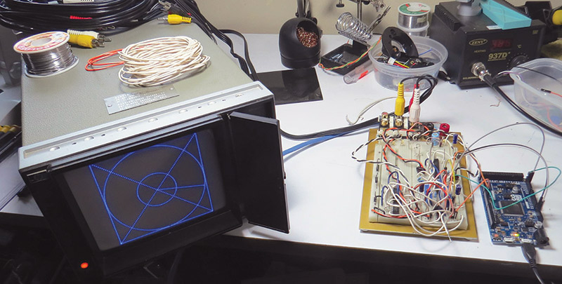
FIGURE 8. My first breadboard prototype.
An extensive AGI Parts List and detailed build and test document can be found with the article downloads. While the Parts List shows Digi-Key part numbers, nothing is exotic, and most of the parts can be sourced from nearly any distributor or surplus channel.
Feel free to substitute alternate parts as needed to utilize your “on-hand stock room.” However, I will add that it did take me a while to get the CA3020 op-amps to behave well running off of a single power supply. If you do substitute the op-amps, be sure to choose alternates that can run from a single power supply while also having stable high frequency (>3 MHz) performance. Slow audio-grade op-amps such as the LM392 will not work.
Once the circuit design was solid, I used Design Spark PCB V8.0 to create a small two-layer PCB (printed circuit board) for the AGI project. Design Spark is a well featured circuit board package that is available free from RS Components. Like all PCB software, Design Spark has a bit of a learning curve.
While it may not be the best choice for someone new to PCB layout, once you understand how “it thinks,” DESIGN SPARK performs quite well.
The completed AGI PCB is seen in Figure 9.
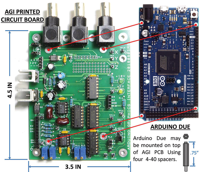
FIGURE 9. AGI circuit board.
Since I wanted to keep things simple and easy to build, I opted to use only through-hole components for this project. I made the AGI PCB a little larger than a standard Arduino board so that the Due could be easily mounted on top of the AGI circuit board using 4-40 spacers.
Figure 10 shows that the connections between the AGI and the Due are easily accomplished with just a few wires.
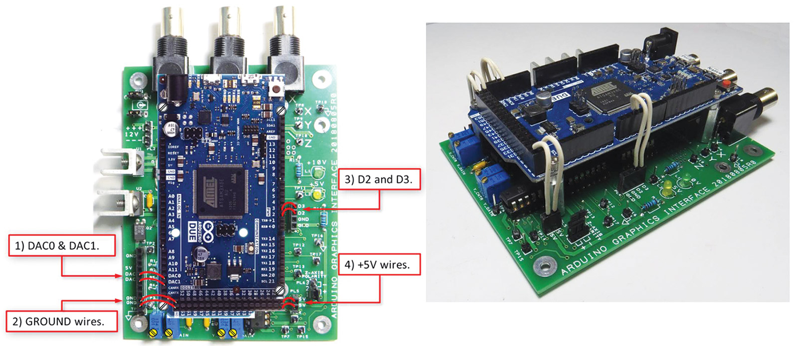
FIGURE 10. Connecting the AGI to the Due.
With this scheme, you remain free to add any shield board that you might need atop the Due. I found the PCB version of the AGI provided a huge performance improvement over my earlier hand-wired builds.
The large bottom layer ground plane on the PCB greatly reduced the noise sneaking into the analog circuits which improved overall image quality. You will find a complete set of Gerber PCB files with the downloads so that you can have PCBs made by your favorite circuit board fab house.
Coming Up in Part 2: Getting Going with the AGI Software
Just like any other Arduino project, the AGI system can be programmed using the Arduino Integrated Development Environment (IDE). In Part 2, we’ll focus on the software by looking at CRT_SCOPE: a test and checkout program that you can use to get your build up and running. We’ll also use this program as a vehicle to demonstrate how easy it is to use XYscope: the Arduino AGI software support library.
You can get ready for Part 2 by downloading and installing the Arduino IDE, Due board definition files, Due timer library, and the AGI library. If this is your first Arduino Due project, I suggest you start out with some basic “hello world” and “blinking LED” test programs to get the IDE set up, compiling, and properly connected to your Due. Check out the References for links to the IDE and a few others that you might find interesting.
See you next time! NV
AGI Oscilloscope Requirements
Overall plot quality is influenced by the quality and performance of the oscilloscope and CRT used. This project works well only with analog oscilloscopes; digital scopes will only produce poor looking output.
There are many analog scopes manufactured by Tektronix, HP, Phillips, Leader, GW-Instek, and others that will work well. Used models are often available starting at less than $50. Look for these key features as you evaluate scope candidates:
- Screen size: Larger is better!
- For best display quality, scope frequency response should be 10 MHz or more.
- Scope must support an X-Y operating mode.
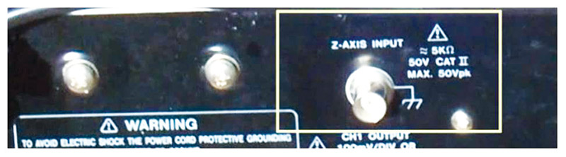
— Scopes that support XY mode typically have panel markings that clearly show XY inputs and settings.
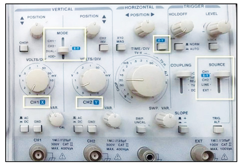
- Scope must have a Z axis or “Intensity Drive” input.
— Check the rear panel of the scope to find this feature.
Parts List
| ITEM # |
REF DESIGNATORS |
QTY |
VALUE/NOTES |
PACKAGE |
| 1 |
C10, C12 |
2 |
470 pf |
DSC |
| 2 |
C11, C13, C14, C15, C16, C4, C5, C8, C9 |
9 |
.1 µF |
DSC |
| 3 |
C2, C7 |
2 |
330 µF |
DSCV |
| 4 |
C3, C6 |
2 |
47 µF |
DSCV |
| 5 |
D1 |
1 |
1N4004 |
DIOD05 |
| 6 |
L1, L2 |
2 |
LED 3 MM GRN |
DSC |
| 7 |
P1, P2, P3 |
3 |
Can use chassis mnt BNC |
USER |
| 8 |
PL1 |
1 |
Can use soldered wire |
SIP |
| 9 |
PL2 |
1 |
Can use soldered wire or alternate connector |
DSC |
| 10 |
PL3 |
1 |
Can use soldered wire |
SIP |
| 11 |
PL4 |
1 |
Can use jumper wire |
DSC |
| 12 |
PL5 |
1 |
Can use soldered wire |
DSC |
| 13 |
PL6 |
1 |
Can use jumper wire |
DSC |
| 14 |
Q1, Q2 |
2 |
IRFD9120 |
DIL |
| 15 |
R1, R11, R4, R8 |
4 |
4.7K |
DSC |
| 16 |
R10, R13 |
2 |
10K |
USER |
| 17 |
R12, R2, R3, R5 |
4 |
10K |
DSC |
| 18 |
R14, R6 |
2 |
100K |
USER |
| 19 |
R15, R16 |
2 |
1K |
DSC |
| 20 |
R7 |
1 |
220 |
DSC |
| 21 |
R9 |
1 |
1.5K |
DSC |
| 22 |
SW1 |
1 |
|
USER |
| 23 |
TP1, TP10, TP11, TP12, TP13, TP14, TP15, TP16, TP17, TP18, TP2, TP3, TP4, TP5, TP6, TP7, TP8, TP9 |
18 |
OPTIONAL |
DSC |
| 24 |
U1 |
1 |
LM317 |
DSC |
| 25 |
U2 |
1 |
LM7805 |
DSC |
| 26 |
U3, U4 |
2 |
CA3240 |
DIL |
| 27 |
U5 |
1 |
CD4066 |
DSC |
| 28 |
U6 |
1 |
CD1013BE |
DSC |
| 29 |
U7 |
1 |
74HC00 |
DIL |
| 30 |
U8 |
1 |
74LS14 |
DIL |
| 31 |
PC1 |
1 |
20180805R0 |
2-LAYER |
| 32 |
CBL1 |
3 |
BNC CBL TO SCOPE (builder supplied) |
CBL |
Downloads
What’s in the zip?
BOM
Build Doc