The first three episodes of this mini-series described the basic nature, behavior and applications of light and light-beam manipulators such as mirrors, prisms, lenses, and fiber optic cables, with particular regard to their use in modern optoelectronic systems. This concluding episode describes the basic (atomic level) operating principles of LEDs and lasers, with particular emphasis on modern laser diodes.
LEDs and LASERs
INTRODUCTION
The two basic types of light-generating devices most widely used in modern optoelectronics are the LED and the laser. (The word LASER is an acronym for Light Amplification by Stimulated Emission of Radiation.)
LEDs and lasers differ in two major respects. First, the LED is a semiconductor device that emits light as a consequence of a current-in, photons-out power conversion process, whereas the laser is a tuned-cavity resonator device that may use a gas, liquid, or solid substance as its active medium and emits light as a result of a photon multiplication process.
The second major difference between the two types of devices is that the LED emits broad-band light in which its photons are randomly-generated and are not directly phase-related, whereas the laser emits a stimulated narrow-band coherent type of light in which its emitted photons are — at the moment of their birth — of the same wavelength and phase as their parent photons.
Because of its coherence, the laser light can be focused into a far smaller spot than that of a LED, thus enabling it to generate very high local power densities. A perfect 0.5mW IR laser beam can, for example, be focused into a minute spot measuring only 1.6µm in width (roughly equal to 1/30th of the width of a human hair), in which the IR power density has a value of about 12kW/cm2 within the focused area.
To begin to understand the basic light-generating principles of LEDs and lasers, it is necessary to first learn some basic facts about the nature of atoms and about photon generation, as follows.
ATOM AND PHOTON BASICS
All solids, liquids, and gases are composed of chemical elements, of which there are 109 different known kinds. Each of these elements are made up from clusters, chains, or lattices of atoms, and the atom is thus the basic building block of all matter.
All atoms take the basic form illustrated in Figure 1 and consist of a positively-charged central nucleus (made up of protons and neutrons) that is surrounded by a number of bands of orbiting negatively-charged electrons. Normally, the positive nucleus charge and the negative electron charge balance one another, thus giving the atom a neutral overall charge; the atom is said to be stable under this condition.
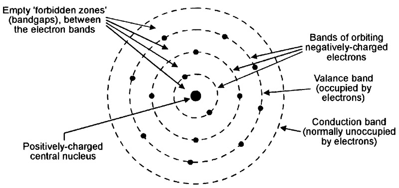
FIGURE 1. Basic form of an atom.
Within the atom, each orbiting electron has a finite kinetic energy value, which determines the distance of its band’s orbit from the central nucleus; the individual electron bands are thus known as energy bands; their energy is measured in electron-Volt (eV) units. Electrons orbiting in energy bands close to the central nucleus have lower energy values than those in the outer bands. The atom’s outer electron-occupied energy band is known as the valence band.
Beyond the atom’s valence band lays a normally-empty high-energy conduction band. If an electron that is orbiting in the valence band gains enough extra energy, it moves upward into the conduction band but, as it does so, it leaves behind a positively-charged hole in the valence band; the energy-gain process thus creates an electron-hole pair. The atom is said to be in a quisi-stable or excited state under this condition. When the atom is in this excited state, an electron will readily move downward from the conduction band into the valence band if it loses sufficient energy, and anihilates the valance band’s positively-charged hole in the process.
In a piece of matter composed of many atoms, the atoms may be linked together in a matrix-like way via their individual conduction bands. In this case, electrons that are not tied to specific atoms (free electrons) may travel freely through the material via the linked conduction bands.
The spaces between the atom’s energy bands are known as forbidden zones or bandgaps. Electrons can not exist in forbidden zones, but can — if subjected to sufficient energy change — jump through them to reach an adjacent energy band.
When an electron jumps downwards through a bandgap (from the conduction band to the valence band), it loses an amount of energy equal to the difference between the two energy band eV values, and this loss is accompanied by the emission of a sub-atomic particle (such as a phonon or photon) with an identical energy value.
From the optoelectronics point of view, all useful photon and electron activity takes place in the vicinity of the atom’s valence and conduction bands, and all such activity can thus be represented by simple energy-level diagrams such as those shown in Figures 2 and 3, each of which depicts a narrow ‘slice’ section taken through the two bands.
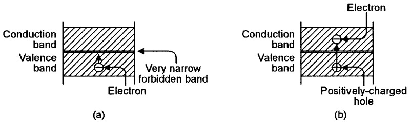
FIGURE 2. Energy-level diagrams relating to a conductor such as copper. (a) An electron can easily move upwards from the valence band, but (b) leaves a positively-charged hole behind.
Figure 2(a) shows the basic energy-level diagram of an atom of a conductive material such as copper. Here, the forbidden zone is so narrow that the valence and conduction bands almost merge into one another, and electrons can —under the influence of an external potential — easily move into the conduction band from the valence band, in which case, the vacated valence position is filled by a positively-charged hole, as shown in Figure 2(b).
Once the electron enters the conduction band, it is no longer bound to the atom, and is free to travel through the conductive material (via the linked outer bands of adjacent atoms) as an electric current.
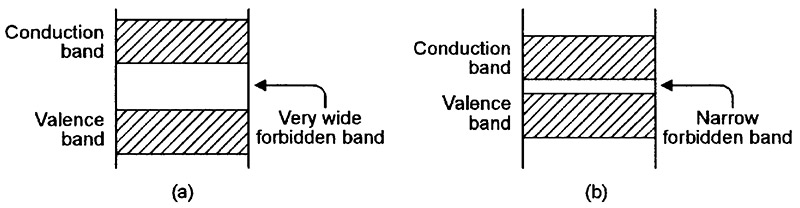
FIGURE 3. Energy-level diagrams relating to (a) a typical electrical insulator and (b) a typical semiconductor.
Figure 3(a) shows the energy-level diagram of an atom of a typical insulation material. Here, the forbidden zone is very wide, thus blocking the flow of electrons into the conduction band and preventing the flow of current through the material.
Finally, Figure 3(b) shows the energy-level diagram of an intrinsic (naturally-occurring) semiconductor material such as silicon, which has a narrow forbidden zone and thus has conduction characteristics mid-way between those of a conductor and an insulator. Unlike a normal conductor, however, the semiconductor’s resistance has a negative (rather than positive) temperature coefficient.
LED OPERATING PRINCIPLES
Conventional LEDs work in the same basic way as normal silicon junction diodes, but use special semiconductor materials to produce the light-emitting diode’s photon-generating characteristics.
Silicon junction diodes are based on two different extrinsic (artificially modified) types of crystalline silicon; one type is very lightly doped with a material such as phosphorus, which has the effect of adding a number of spare electrons (donors) to the conduction band of the silicon’s crystal lattice, as shown in the material’s energy-level diagram of Figure 4(a); this material is known as an n-type semiconductor, since it carries an excess negative charge. The other type of silicon is lightly doped with boron, which has the effect of adding a number of spare holes (acceptors) to the valence band of the silicon lattice, as shown in the energy-level diagram of Figure 4(b); this material is known as a p-type semiconductor, since it carries an excess positive charge.
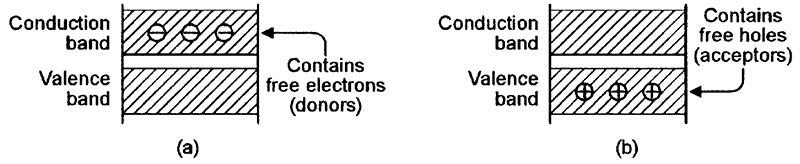
FIGURE 4. Energy-level diagrams for (a) n-type and (b) p-type semiconductors.
In a junction diode, the n-type and p-type materials are fused together in the manner indicated in the greatly simplified diagram of Figure 5, which also shows the diode’s circuit symbol.
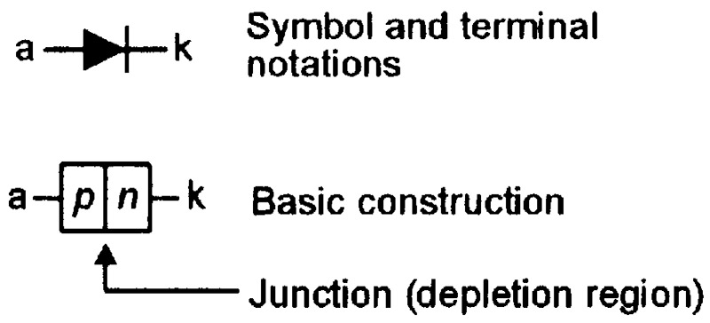
FIGURE 5. Symbol and basic construction of a silicon junction diode.
Since both halves of the diode are made from the same basic material (silicon), the device is often called a homojunction diode. Figure 6 shows the diode’s energy-level diagrams under (a) unbiased, (b) reverse biased, and (c) forward biased conditions. In these diagrams, the junction between the n-type and p-type materials is named the depletion region.
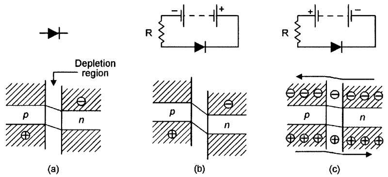
FIGURE 6. Energy-level diagrams of a silicon junction diode under (a) unbiased, (b) reverse biased, and (c) forward biased conditions.
The energy level of the junction diode’s positively-charged p-type material is inherently higher than that of the negatively-charged n-type material, as shown in Figure 6(a). Consequently, if the diode is reverse biased as shown in Figure 6(b), the energy level difference between the p-type and n-type material becomes even greater, inhibiting any significant flow of electrons or holes between the two materials via the depletion region.
Under this reverse-biased condition, the only currents that flow through the diode are small temperature-sensitive leakage ones and (if the junction is directly exposed to an external light source) small photon-induced currents.
Alternatively, if the diode is forward biased as shown in Figure 6(c), the energy level difference between the p-type and n-type material falls to near-zero at a forward bias value of about 0.6V, enabling electrons and holes to flow freely between the two materials via the depletion region. An electric current thus flows through the forward biased junction; it actually flows through the covalence bands (valence bands that are linked in adjacent atoms) within the silicon matrix, and often generates a phonon particle at the moment of exchange; the phonon energy is dissipated within the crystal lattice as vibrant heat.
Conventional LEDs use the same basic homojunction form of construction and work in the same basic way as normal junction diodes, but use special semiconductor materials (rather than silicon) that emit photons (rather than phonons) when forward current flows through the material’s lattice. Figure 7 shows the circuit symbol and the basic construction of a conventional LED, and Figure 8 shows the LED’s energy-level diagram under forward biased operating conditions.
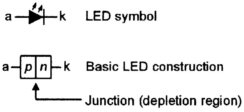
FIGURE 7. Symbol and basic construction of a conventional LED.
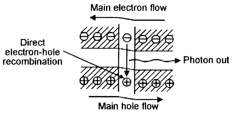
FIGURE 8. Energy-level diagram of a conventional LED under forward biased operating conditions.
In Figure 8, when current is flowing through the forward biased junction, most free electrons and free holes travel through the depletion (junction) area in the normal way, but some electrons don’t have enough energy to stay in the conduction band and drop down (via the forbidden bandgap zones of individual atoms) into the valence band and annihilate a hole.
The electron energy lost in this process is converted into a photon, which is radiated from the LED as a light particle. LED electrical power-in to optical power-out conversion efficiency is low, typically in the range 0.01% to 1.5%, and is greatly influenced by the photon’s wavelength.
The LED’s photon wavelength, λ (in nm) is dictated by the bandgap energy (eV, = the difference between the valence and conduction band energy values) of the LED’s semiconductor material, and these two parameters are related by the easily-remembered formula λ = 1240/eV, and eV = 1240/λ. Thus, a LED that generates a red output at a wavelength of 645nm has a bandgap energy value of 1.92 eV.
Figure 9 shows some practical LED wavelength/bandgap-energy relationships values, together with basic details of the types of semiconductor material used to make various LEDs. The basic semiconductor material determines the approximate energy value of the bandgap; the actual value is fine-tuned by suitably doping the material.
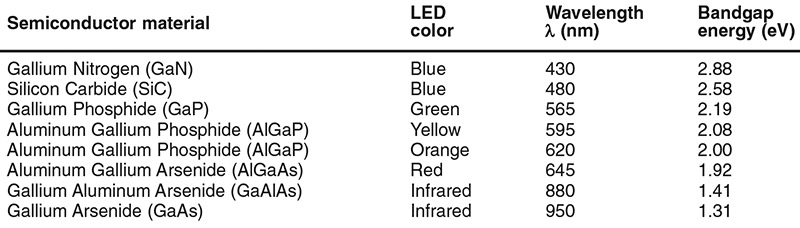
FIGURE 9. Table of LED wavelength/bandgap-energy relationships.
Note that the bandgap values quoted in Figure 9 are ‘mean’ (rather than absolute) ones. In reality, the bandgap energy of an atom is not fixed, but varies from moment to moment, depending on the instantaneous depths of individual electrons within its valence-conduction bands. These energy variations are fairly small (usually within ± 2% of mean), but (since a photon’s wavelength is directly related to bandgap energy) cause the LED’s output to have a finite ‘minimum spectral bandwidth’ value.
The simple LED described earlier in this section is a surface-emitting homojunction type that uses the same basic material on both sides of its junction. In practice, many modern LEDs use different materials on the two junction sides, and are thus known as heterojunction LEDs; most such LEDs have two-stage internal junctions, and are known as double-heterojunction LEDs. Some special LEDs (designed to easily interface with fiber optic cables) are ‘edge-emitting’ types that emit a narrow beam of light from the side of the semiconductor material, rather than a broad beam from its face.
LASER BASICS
LEDs emit individual photons in a quite random or spontaneous fashion, whereas lasers emit photons in a stimulated fashion in which the birth of each new photon occurs on the arrival of a parent photon. In a laser, each new photon is — at the moment of its birth — a duplicate of its parent photon, with the same basic wavelength and (more importantly) an identical phase. Light composed of in-phase photons is known as coherent light, and can be focused far more sharply than other types of light.
Figure 10 shows six typical ‘random’ photon waveforms emitted by a LED, together with their composite light output waveform (equal to the sum of the six photon waveforms), and Figure 11 shows a similar set of coherent waveforms emitted by a laser. Each diagram spans a 10pS (10 picosecond) time interval (1pS = 1 millionth of a µS) and depicts six newly-generated IR photons with wavelengths of 850nm (= a frequency of 353,000MHz) and an amplitude value of ‘1 light unit.’ The typical relative position of each photon is indicated by a small black dot.
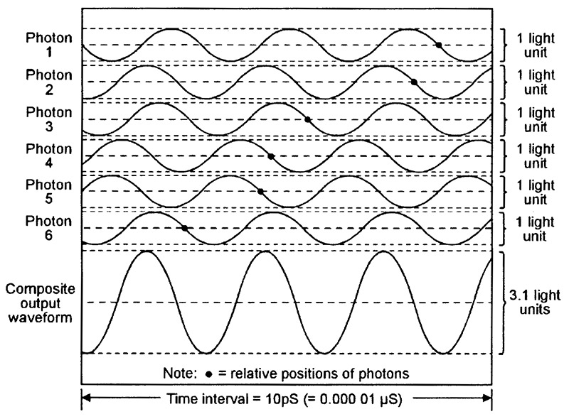
FIGURE 10. Six typical random (spontaneous) photon waveforms emitted by a 850nm IR LED, together with their composite ‘light’ waveform.
Note in Figure 10 that the waveforms of photons 1 and 5 are in exact anti-phase and thus have a combined value of zero, and that all remaining photon waveforms are out of phase with one another and (in this particular case) have a combined value of 3.1 light units. In practice, the pattern of the six photon waveforms changes continuously as new photons enter the time frame from the left and others leave the frame on the right, and this causes the instantaneous phase and amplitude of the composite output waveform to vary over a wide range. As a consequence of these rapid phase and amplitude variations (intermodulation), the LED’s light output is very impure and has a fairly wide spectral bandwidth.
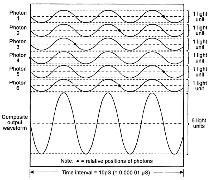
FIGURE 11. Six typical coherent (in-phase) photon waveforms emitted by a 850nm IR laser, together with their composite ‘light’ waveform.
By contrast, the six laser-generated photon waveforms shown in Figure 11 are all exactly in-phase, and the composite output waveform thus has a fixed phase relationship and has a constant amplitude of 6 light units. The laser’s light output is thus very pure, with a very narrow spectral bandwidth. Typically, a modern 850nm IR LED has a half-power spectral bandwidth (i.e., the bandwidth at which the light power output falls to half of its maximum value) of about 80nm. Modern 850nm laser diodes, on the other hand, have typical half-power spectral bandwidths of 0.5nm to 5nm, and their light outputs are thus far purer than those of LEDs.
LASER OPERATING PRINCIPLES
The basic atomic operating principle of the laser is in some ways similar to that of the LED. In both cases, a photon is generated in an excited atom when an electron in its conduction band loses energy and drops down into the atom’s valence band, annihilating a hole and generating a photon in the process. In the LED, this process occurs randomly, when the electron’s energy decays below a critical value.

In the laser, however, the process is initiated by photonic stimulation, in which an external photon with an energy value equal to that of the atom’s bandgap enters the atom’s bandgap and, by a quantum process known as negative absorption, makes the electron lose energy and drop down into the atom’s valence band, thereby annihilating a hole and generating an identical photon.
Figure 12 illustrates the basic atomic operation of the ‘lasing’ process.
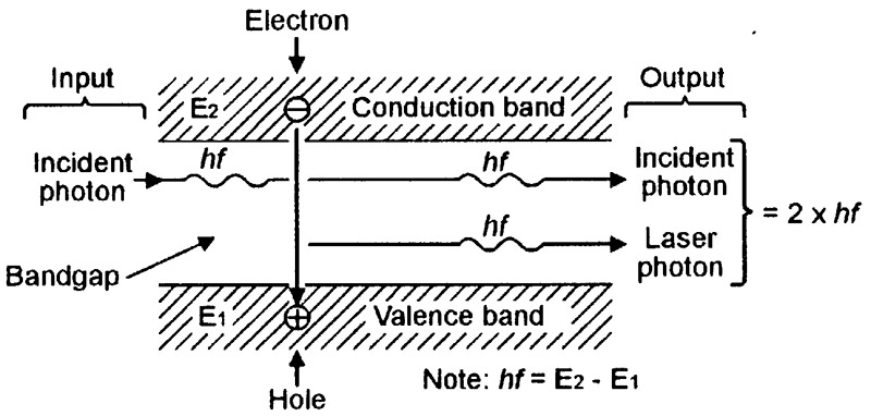
FIGURE 12. Basic atomic operation of the lasing process.
Here, the incident (arriving) photon, which has an energy value identical to that of the atom’s conduction-valence bandgap (= hf), enters the bandgap from the left side of the diagram and makes the electron drop down and annihilate the hole, thereby generating a new ‘laser’ photon, which also has an energy value of hf. The incident and laser photons, which have identical phase and frequency-wavelength values, then emerge together on the right side of the diagram.
Note from the above descriptions that lasing action can only occur if the atom is in an excited state at the moment that the incident photon arrives, and if the incident photon’s energy value equals that of the atom’s bandgap. Also note that, if lasing action does occur, the excited atom gives an effective 2:1 overall photonic power gain, but drops out of the vital ‘excited’ state after generating a single photon.
In a practical laser, the actual lasing medium (which contains vast numbers of atoms capable of giving lasing action) may take the form of a gas, a liquid, or a solid material, in which the lasing atoms may be raised into an excited state by electrical, chemical, or optical means.
In laser jargon, the process of feeding energy into the medium to hold its atoms in an excited state is known as pumping, and the situation in which most of the medium’s atoms are in the excited state is known as a situation of population inversion. Thus, the medium must be pumped to create population inversion, which is a prerequisite of laser action. Lasing action can only begin if the medium’s energy input exceeds a certain pumping threshold value; to give continuous lasing, the medium must be continuously pumped.
Figure 13 shows the basic elements of a complete laser unit. One of these is the actual lasing medium, which must be reasonably translucent. Another is a power supply that is used to pump the medium into a state of population inversion and initiate the lasing action. The final unit is a resonant optical cavity, made of two mirrors set at opposite ends of the lasing medium so that photons can repeatedly bounce back and forth through the medium; one mirror is fully reflective; the other has a small (equal to about 1% of the mirror’s surface area) translucent hole in its center.
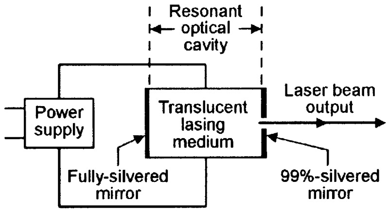
FIGURE 13. Basic elements of a complete laser unit.
In Figure 13, lasing begins when — with the medium pumped up to its threshold value — a suitable internally- or externally-generated incident photon hits an excited atom and initiates the birth of an identical photon. This pair of photons then travel to the right, hit the end of the cavity, then reflect back and forth through the cavity, repeatedly passing through the lasing medium and initiating the generation of more photons in each pass, so that the photon flow rapidly builds up into a flood that can easily be controlled via the power supply.
Photons that strike the translucent hole at the center of the cavity’s right-hand mirror emerge (bleed off) from the laser unit in a narrow and coherent beam that can be focused into a minute and intense spot by an external lens.
The optically-resonant cavity is a vital part of the laser system. It is highly wavelength-selective and gives high optical gain (resonance) only to signals with an integer number of half-wavelengths that fit exactly into the cavity’s optical length (equal to the product of its physical length and refractive index value).
The cavity’s length is inevitably many times longer than the (roughly 1000nm) optical wavelength of the basic laser beam, and it thus has a huge number of optical operating modes (wavelengths at which resonance may occur). In a cavity with an optical length of 2mm, for example, the first mode occurs at a wavelength of 4mm, the 10th at 0.4mm, the 100th at 40µm, the 1000th at 4000nm, the 4705th at 850.16nm, the 4706th at 850nm (a commonly-used IR wavelength), and the 4707th at 849.8nm.
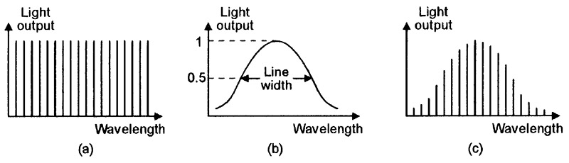
FIGURE 14. Typical frequency response of (a) a laser’s optically-resonant cavity, (b) the unfiltered output of a lasing medium, and (c) the resulting laser-beam output of the cavity.
The optical cavity’s frequency response thus consists of a series of sharp comb-like peaks (known as mode lines in laser jargon), as shown in Figure 14(a). In the above example, at wavelengths around 850nm, these peaks are spaced roughly 0.2nm apart. In some practical lasers (including many laser diodes), the lasing medium’s basic (unfiltered) output has the type of frequency response shown in Figure 14(b), and spans dozens of these peaks; in such cases, the cavity’s laser-beam output thus has the type of frequency response shown in Figure 14(c).
In laser jargon, the half-power spectral bandwidth of a laser output is called its linewidth. Lasers with linewidths that fit into a single mode line are known as single mode lasers; ones with linewidths that span more than one mode line (as in the case of Figure 14(c)) are known as multi mode lasers.
All practical lasers have finite linewidths and (since they contain a spectrum of frequencies) their beams can remain fully coherent (in-phase) for only a limited number of wavelengths after their initial creation. This dimension is known as the beam’s coherence length, and equals the square of the beam’s mid-value wavelength divided by its linewidth. Thus, an 850nm beam with a linewidth of 2nm has a coherence length of only 0.36mm.
LASER TYPES
The world’s first working optical laser was demonstrated by an American, Theodore Maiman, in mid-1960. Known as a ruby laser, it has the basic form shown in Figure 15(a) and consists of a small rod of synthetic ruby crystal (the lasing medium), with mirrored ends that form the optical cavity; the rod is surrounded by an electrically powered helical flash tube, which acts as the medium’s energy pump. When the flash tube is operated, its white light pumps the rod’s atoms into an excited state, and a brief burst of lasing action commences a few milliseconds later, causing a brief pulse of red laser light to emerge from one end of the tube.
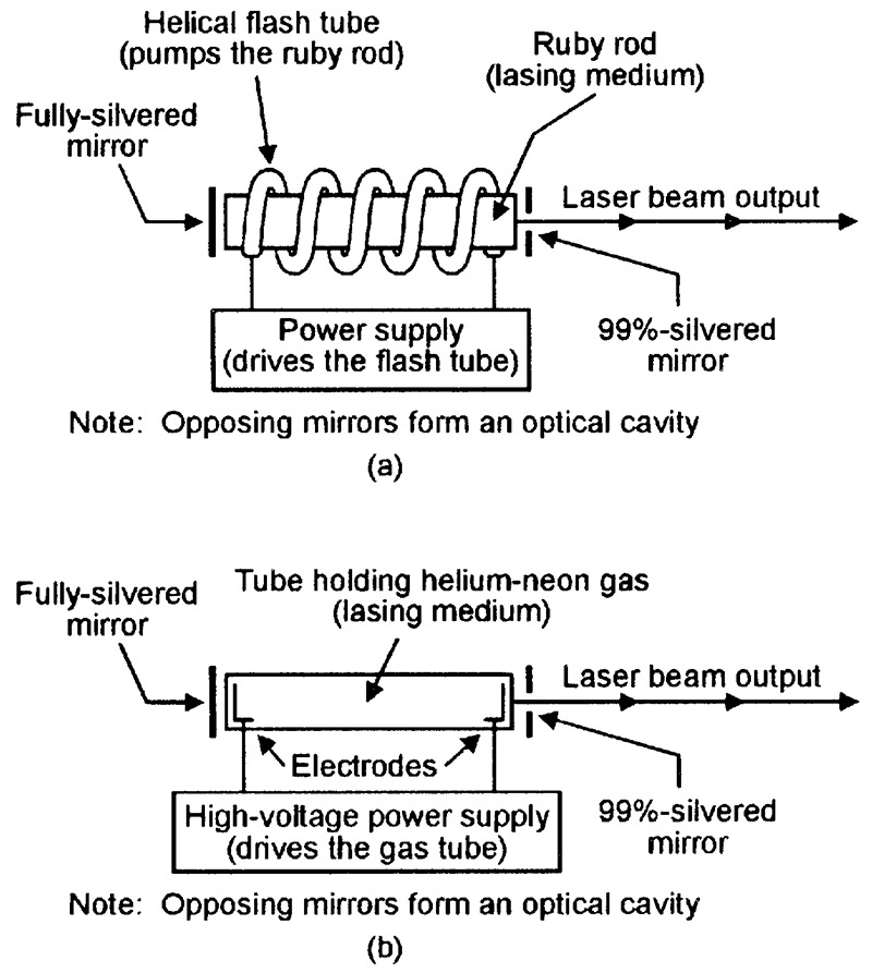
FIGURE 15. Basic functional diagrams of (a) ruby and (b) helium-neon lasers.
The ruby laser provides only brief pulses of laser light. The first laser to give continuous-wave (cw) operation was the helium-neon (He-Ne) gas laser, which was first demonstrated in late 1960 and has the basic form shown in Figure 15(b). Here, the high-voltage supply pumps the gas molecules into an excited conductive state in which sustained lasing action takes place (typical supply voltages are 8kV for starting, 1.5kV when running); lasing takes place primarily at a wavelength of 632nm and the device thus generates a bright red laser beam.
He-Ne lasers are still widely used; most have maximum optical output powers in the range 0.5 to 10mW; the outputs have typical linewidths of a mere 0.002nm and beam coherence lengths of 200mm. Some modern He-Ne lasers have outputs that can be electronically modulated (but not pulsed) at frequencies up to 1MHz.
Many other types of laser have appeared since 1960. Most have severe practical disadvantages (such as very brief working lives, excessive cost, fragility, or bulkiness, or severe thermal operating requirements) or are meant only for laboratory or military use. Some are designed specifically for use in optical welding or cutting operations, and are not suitable for use in general ‘electronic’ applications. Most have input-to-output power conversion efficiencies of only 0.001 to 0.5 percent (a 1mW He-Ne laser, for example, typically needs an input power of 20W).
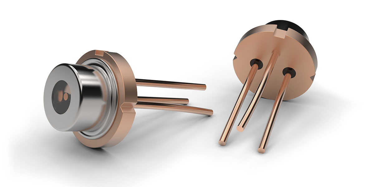
The laser best suited to use in general electronic applications is the so-called ‘laser diode,’ which (in most low-power types) acts like a laser version of the double heterojunction side-emitting LED, with a built-in resonant optical cavity. It is compact, robust, has a typical working life of 50,000+ hours, and is reasonably easy to use.
A laser diode produces a cw laser beam that can be pulse or analog modulated at frequencies up to many hundreds of MHz, has a typical input-to-output power conversion efficiency of 1.5%, and is commercially available in versions giving maximum optical power outputs ranging from 0.1mW to several watts, at a variety of red and infrared wavelengths. Single mode types have typical linewidths of less than 0.5nm; multi mode types have typical linewidths in the range 2nm to 5nm.
Figure 16(a) shows the typical supply-current to optical-output-power graph of a normal LED, and Figure 16(b) shows that of a laser diode. The LED’s graph is quite linear, and the optical output power is directly proportional to the LED’s supply current value. The laser diode has a more complex performance graph; at supply currents well below the lasing threshold value, it acts like a normal LED and generates random photons, but at currents well above the lasing threshold, it gives true lasing action and generates coherent photons. When operating at the actual lasing threshold level, it generates both random and coherent photons.
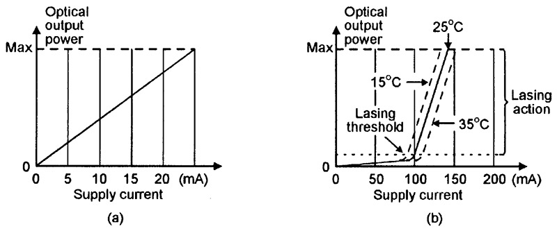
FIGURE 16. Typical supply-current to optical-output-power graphs of (a) a normal LED and (b) a laser diode.
Note in Figure 16(b) that, at any fixed lasing current values, the optical output power is very sensitive to variations in the laser diode’s temperature. Most practical laser diode units (modules) incorporate sensing and control circuitry that stabilizes the optical output power by auto-adjusting the lasing drive current. Most modern units of this type use special laser diodes that have an integral monitoring photodiode; Figure 17 shows a four-pin version of such a unit, together with a simple way of using it as a cw laser transmitter.
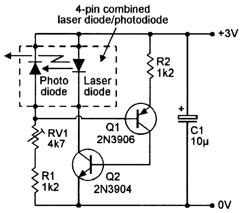
FIGURE 17. Simple way of using a four-pin combined laser diode/photodiode unit in a cw laser transmitter.
In Figure 17, the photodiode’s reverse current (and thus the voltage on Q1 base) is proportional to the laser beam’s intensity. Q1 acts as a voltage-controlled constant-current generator that supplies base drive to Q2 which, in turn, provides drive current to the laser diode.
The overall action is such that, if the laser intensity falls below a value preset via RV1, the photodiode-derived Q1-base voltage also falls, thereby increasing Q1’s current drive to Q2 base and causing Q2 to increase the drive current to the laser diode, which responds by increasing its laser intensity.
The reverse process occurs if the laser intensity rises above the preset value. The circuit thus auto-regulates the laser beam intensity.
Figure 18 shows a basic way of using the four-pin combined laser diode/photodiode unit in a pulse modulated cw laser transmitter.
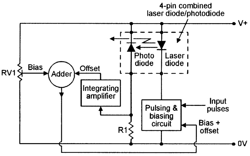
FIGURE 18. Basic circuit of a pulsed cw laser transmitter using a four-pin combined laser diode/photodiode unit.
Here, the pulsed output of the laser-monitoring photodiode is converted into a DC offset voltage via an integrating amplifier, is combined with an RV1-derived pre-set DC bias voltage via an adder, and is fed to one input of the laser-driving pulsing and biasing circuit, which has its other input driven by external pulse-coded waveforms. The RV1-derived DC bias voltage is set so that — in the absence of input pulses — the laser diode is biased at its lasing threshold value (rather than fully off), thus giving a very fast switching action.
LASER APPLICATIONS
WARNING. Sensible safety precautions must always be taken when using lasers; the output beam of even a 0.5mW type can cause severe optical damage if aimed (deliberately or accidentally) at a human eye.
Low-power (up to 5mW) lasers are readily available in ‘module’ form, comprising the actual laser plus its drive circuitry and optics. They have a multitude of practical applications. Simple cw types, using the basic type of circuit shown in Figure 17, can — if generating a visible red beam — be used as laser pointers, spirit levels, or alignment aids, or as the basis of bar-code readers. Alternatively, infrared types can be used in a wide range of security applications, activating an alarm or initiating some other action when a person, animal, object, vehicle, smoke, or fog breaks or reflects the beam. When reflected from a solid surface, the cw beam can also be used to detect minute vibrations of the surface.
All CD and CD-ROM players incorporate a small cw laser module that (aided by various lenses and servo-drivers) automatically scans the spinning CD and picks out the information contained in the tracks (which are spaced only 1.6µm apart) of its coded sub-surface data pits, which are each a mere 0.1µm deep and 0.8µm to 3.5µm long, retrieving the data at a rate of over 4,000,000 bits per second.
Laser modules that are designed for use as modulated cw types can be used in all of the types of ‘security’ applications already mentioned, plus various speed- and distance-measuring applications. They are particularly useful in long-haul fiber optic communication and data-transfer systems, in which (because of their very small spectral bandwidths) they can greatly outperform LEDs.
Single mode IR laser diodes, for example, have spectral linewidths of only 0.5nm, compared to 80nm for LEDs, and their signals thus suffer far less material dispersion than those of LEDs when traveling through long lengths of fiber optic cable. NV