An Invention that Changed the World
Life would not be the same without the transistor, which was invented just over seven decades ago. It is considered by researchers and historians to be the most important invention of the 20th century, leading to groundbreaking advances in computing, communications, medicine, and practically every technically related field. Without it, developments such as the personal computer, cellphones, the GPS system, pacemakers, hearing aids, and the Internet would not exist.
It started with a Bell Telephone Laboratories program of basic research on solid-state physics in 1936 that produced a replacement for the vacuum tube in the 1950s and eventually gave us integrated circuits and the microprocessor. It spawned a huge semiconductor industry generating hundreds of billions of dollars in sales.
However, behind this story of invention is one of collaborative genius, serendipitous mishaps, clashing egos, and secret research. In this article, we’ll look back on this period that launched the serious study of solid-state devices. We’ll examine the contributions of the personalities and organizations involved, as well as the impetus that led to this landmark invention. We’ll also look at the early history of semiconductors, as well as the impact of vacuum tubes on transistor development.
My fascination with electronics began at an early age when I received a Standard Radio Telegraph Signal Set from my parents.
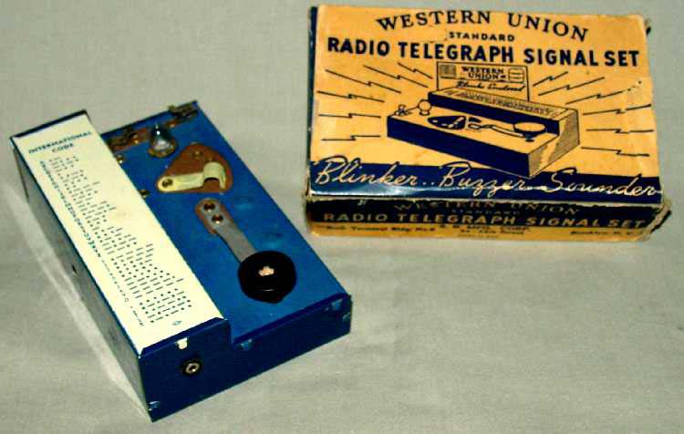
Its blue painted metal case had the Morse code printed in white on top, a simple key, a light bulb, an internal buzzer, and it operated on two D cells. It was fascinating for a while, but my interest really took off when I decided to make my own crystal radio set like the one in Figure 1.
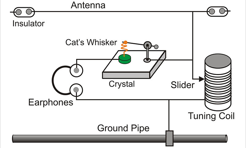
FIGURE 1. My first crystal radio set. It employed a galena crystal with a cat whisker for detection, a homemade coil with slider for tuning, and a pair of surplus headphones. This common circuit didn’t use a tuning capacitor, but used the capacitance of the antenna to form the tuned circuit with the coil. A good antenna and ground were needed for reception.
This involved winding a coil of copper wire on an old cardboard tube and making a slider for tuning. Getting the costly phones and crystal was the most difficult part. The crystal detector consisted of a small cylindrical piece of galena placed in proximity to a moveable arm which had a spring-like bronze wire called a cat’s whisker that was used to contact the galena.
After I assembled the parts and connected it to a wire antenna and cold water pipe, I listened for a sound. There was nothing! I had heard that you needed to fiddle with the cat’s whisker on the galena face to find the “hot” spot.
After some trial and error, suddenly the sound of a radio station burst through on the headphones. My radio was working!
Little did I know that I was working with one of the first solid-state devices: a predecessor of the point-contact transistor. This was also my first encounter with a semiconductor: galena, the world’s first semiconductor. The galena crystal was the key component in my radio.
This tiny crystal had the seemingly magical ability to modify the complex electrical currents from my antenna and act as a semiconductor to isolate the audio portion of the broadcast radio waves.
In what follows, we’ll have more to say about crystals and point-contact devices. It’s a captivating story about the discovery and understanding of semiconductors and the people and companies involved in the invention of the transistor. To get started, let’s look at some of the early work in the area of semiconductors.
Early History of Semiconductors
According to historians, the first scientist to use the word “semiconductors” was Alessandro Volta in his report to the London Royal Society in 1782. By touching a charged electrometer (a simple charge detector) to different materials, he found that metals caused immediate discharge of the electrometer. On the other hand, dielectrics caused no discharge at all. However, some materials — which he called semiconductors — caused a discharge in a short (but not zero) time.
Research in the semiconductor field at first proceeded extremely slowly, but sped up in the mid-19th century. Much of the early work consisted of just recording the physical properties of these materials. They were generally characterized as materials with resistivities somewhere between insulators and metals.
These first discoveries were done by individuals engaged in pure research who made their results known by writing papers in scientific journals. At this stage, there was no theoretical basis for the observations and no effort was made to put these discoveries to practical use.
In 1833, Michael Faraday was the first to record an effect due to semiconductor behavior when he found that silver sulfide (Ag2S) — unlike metals — exhibited a negative temperature coefficient. Soon thereafter, M. A. Rosenschold in 1835 observed asymmetric conduction in solids. His work was forgotten until it was re-discovered by German physicist, Karl Ferdinand Braun in 1874 (as we’ll discuss later on).
In 1839, Edmond Becquerel discovered the photovoltaic effect that explained how electricity can be produced from sunlight. At age 19, working in his father’s laboratory, he created the world’s first photovoltaic cell by observing a voltage being generated at a junction between a semiconductor and an electrolyte when illuminated. Its main purpose for many years was for the measurement of light — and much later to solar panels.
Years later in 1873, the photoconductive effect was first described by Willoughby Smith, who noted that the resistance of a circuit element made of crystalline selenium decreased upon exposure to light. When such photoconductive material is connected as part of a circuit, it acts as a resistor whose resistance depends on the light intensity. Today, such devices are called photoresistors. Many years later, this work led to the commercial use of photoconductive cells in camera exposure meters.
The mystery surrounding semiconductors began to unravel in 1874 when Ferdinand Braun observed that electrical resistance in metal-sulfide crystals varied with the direction of current flow. Concentrating on galena, Braun found that the current influence was greatest when one of the connecting electrodes was a pointed wire. By discovering the so-called “point-contact electrical-rectifier effect,” Braun had also invented the first crude semiconducting device.
Unfortunately, Braun’s discovery had no practical application until the early 1900s, when American scientist, Greenleaf Whittier Pickard (Figure 2) learned that semiconducting galena crystals could detect radio signals. This knowledge led directly to the development of the first radio receivers, fittingly known as “crystal sets.” These simple devices consisted of a wire aerial, a tuning circuit composed of wire coils, an earphone, and a “detector.”
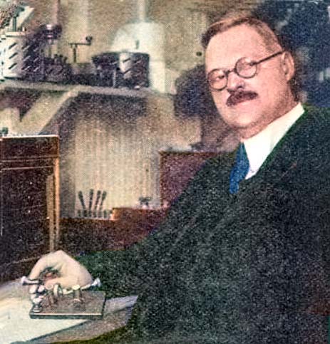
FIGURE 2. Greenleaf Whittier Pickard was a United States radio pioneer and researcher in the early days of wireless. While not the earliest discoverer of the rectifying properties of contact between certain solid materials, he was largely responsible and most famous for the development of the crystal detector: the earliest type of diode detector. This was the key element in many early radio receivers until about 1920 when tubes replaced it.
Detection of the usable audio portion of the aerial micro-current was accomplished by touching a thin, flexible copper wire (fittingly called a cat’s whisker) on the face of the galena crystal until the audible signal was loudest. This crystal detector was the central component of early radio receivers from 1906 to 1920. This device — now known as the point-contact diode — didn’t have any theoretical explanation of its operation until the 1930s.
Although the point-contact crystal diode acted as an efficient detector (provided that periodic adjustment of the cat’s whisker was made), it would not function as an amplifying device. A very real need existed at this time for a device that would not only detect but also amplify weak radio signals and operate without mechanical adjustment.
Lee de Forest (Figure 3) successfully met this need in 1906 with the invention of the thermionic triode tube. Largely due to its subsequent success as an amplifier, work in the solid-state area did not make much progress either theoretically or experimentally during the period from approximately 1910 to 1930.
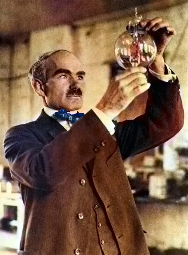
FIGURE 3. Lee de Forest was a United States inventor — the self-described "Father of Radio" — and a pioneer in the development of sound-on-film recording used for motion pictures. He had over 180 patents, but also a tumultuous career; boasting that he made (then lost) four fortunes. He was also involved in several major patent lawsuits and spent a large part of his income on legal bills. His most famous invention in 1906 was the three-element "audion" (triode) vacuum tube: the first practical amplification device. Although de Forest had only a limited understanding of how it worked, it became the foundation of electronics, making possible radio broadcasting, long distance telephone lines, and talking motion pictures, among countless other applications.
From Tubes to Solid-State
Before transistors, most electronic devices such as computers and radios relied on electronic vacuum tubes. They consisted of electrodes in an evacuated bulb through which an electric current could be passed and controlled. This allowed the tubes to function as amplifiers and switches.
In 1904, John Fleming invented a two-element vacuum tube or diode. Fleming’s invention was used in early radio work as a rectifier.
In 1906, de Forest invented the three-element tube or triode by putting a metal grid in the middle of the tube. By changing the voltage on the grid, he could control a strong current through the tube.
This device became the model for later vacuum tubes. It was one of the most important breakthroughs in electronics history — making possible amplification, modulation, and switching — laying the groundwork for commercial radio, television, high-fidelity audio, and the development of the first digital computers.
However, vacuum tubes — also known as valves — were far from perfect. They were large and the heated metal filament that emitted electrons would eventually burn out. Their fragile glass envelope made them easily breakable. A considerable amount of power was required by tubes, so they were very hot to the touch. Computers were eventually built with them, but they were huge and slow.
Over the years, researchers strove to replace tubes with solid-state devices. Some amazing work by a relatively unknown researcher, Oleg Losev seems to have been forgotten in the course of history. His captivating story bears retelling.
Oleg Losev (or Lossev) was a Russian scientist who made significant discoveries in the field of semiconductor junctions in the 1920s. He observed light emission from silicon carbide point-contact junctions, which was essentially the first light emitting diode (LED). He published his results in 1927, proposing the first correct model for LEDs based on the new theory of quantum mechanics. He also solved another mystery.
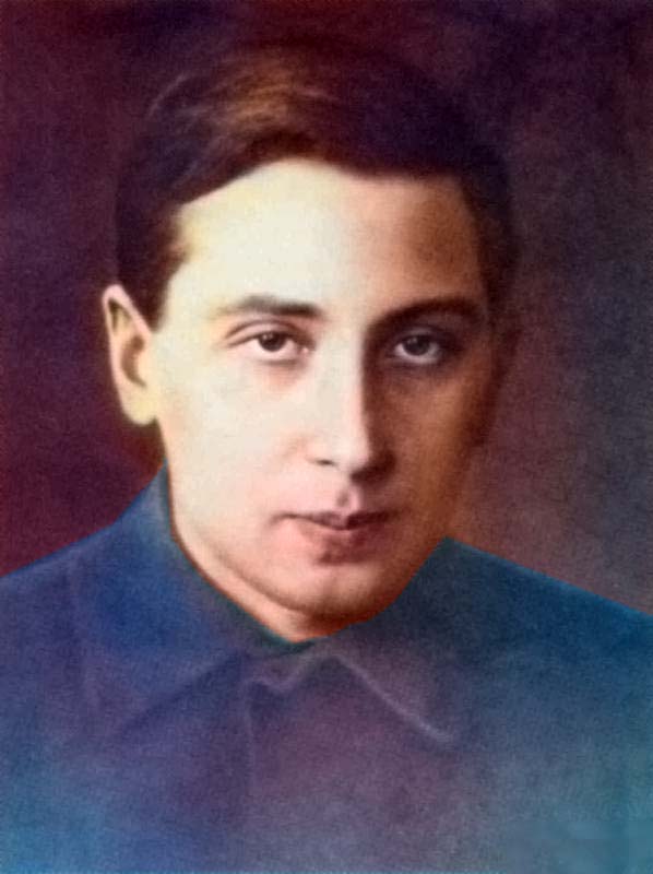
Figure 4. Oleg Losev was a Russian scientist and inventor who made significant discoveries in the field of semiconductor junctions. He published 43 papers and received 16 Soviet patents for his discoveries. He was the first to observe light emission from carbide point-contact junctions (first LED) and proposed the first correct theory of how they worked. He also explored negative resistance junctions and was the first to use them for solid-state amplifiers, oscillators, and radio receivers. His achievements were overlooked until recently.
It was noticed that when a DC bias voltage was applied to a cat’s whisker, in order to increase its sensitivity as a detector in a crystal radio, it occasionally broke into spontaneous oscillation, producing a radio frequency alternating current. This was a negative resistance effect and was noticed in 1909 by William Eccles and Greenleaf Pickard, who paid no attention to it.
In 1923, Losev began studying these oscillating crystals. He discovered that biased zinc oxide crystals could amplify a signal. Losev was the first to exploit negative resistance diodes and he realized that they might serve as simpler alternatives to vacuum tubes. He used these diodes to build solid-state versions of amplifiers, oscillators, and regenerative radio receivers at frequencies up to 5 MHz. This was 25 years before the transistor!
While Losev’s work on LEDs was never commercialized, he had more success with negative resistance diodes and radios. He built over 50 radio receivers incorporating his unusual circuits. Losev’s radios and detectors were exhibited during the 1920s at many European radio technology expositions.
Hugo Gernsback — the famous American publisher and editor — endorsed Losev’s work in sensational terms. Gernsback coined the word “crystadyne” to describe it and wrote a major article in Radio News in 1924 titled A Sensational Invention. He even had a crystadyne radio constructed to Losev’s exact specifications.
Despite Gernsback’s enthusiasm, negative resistance diodes never made an impact. There were problems with the crystadyne crystals, and the best zinc oxide crystals came from the United States which was a problem for Stalinist Russia. Because it could not compete with the performance of current tubes, the crystadyne was ultimately passed over. It was left to Leo Esaki in 1957 to rediscover this important device, now known as the tunnel diode.
Losev’s story is one of what might have been. The world has never heard of him and only knows of unrelated scientists as inventors of the solid-state technology he once used. He had the misfortune to be born in the wrong time and place.
At the end, he found himself trapped in Leningrad besieged by the Germans in 1942. It was reported that he was working on a three-terminal semiconductor amplifier device at the time of his death.
Early Attempts at Transistors
In another effort to replace tubes with solid-state devices, Julius Lilienfeld filed a patent in 1926 for a “Method and Apparatus for Controlling Electric Currents” in which he proposed a three-electrode structure using copper-sulfide semiconductor material. It was a device that relied on changes to an electric field to control the shape and conductivity of a channel in a semiconductor material.
It’s the same principle behind today’s field-effect transistor — the most common type of transistor. However, it’s not clear whether Lilienfeld ever produced such a transistor. Indeed, it is not known if it would be possible to build one based on his patent description.
Later in 1935, Oskar Heil of the University of Berlin (while working at Cambridge University) obtained a British patent for a proposed field-effect transistor entitled “Improvements in or Relating to Electrical Amplifiers and other Controlled Arrangements and Devices.” This device consisted of a thin layer of semiconductor across which a potential difference was established by means of two electrodes at different potentials connected at either side.
A third control electrode (insulated from the semiconductor) would then be used to modulate the resistance of the semiconductor layer, thereby controlling the flow of current in an external circuit connected between the two electrodes. Although the patent was granted, no records exist to prove that Heil actually constructed functioning devices.
The Rise of Industrial Science
Around 1906, there was a big problem looming for the American Telephone & Telegraph Company (AT&T). Up to now, the company had grown and prospered as a result of Alexander Graham Bell’s inventions and patents. However, these patents were running out at the turn of the century and the business was being gobbled up by thousands of local phone companies. In desperation, AT&T brought its former president, Theodore Vail, out of retirement to help it fight off the competition.
Soon thereafter in 1907, the determined new president committed AT&T to building transcontinental telephone lines as a key effort in his goal of establishing universal service. In this commitment, he believed that his outstanding men could overcome any technical problems. There was, however, one major hurdle.
Beyond a few hundred miles, the feeble voice signals of the telephone became drowned in static. For his dream to succeed, his company badly needed amplifiers (voice repeaters) along the way to rejuvenate the attenuated signal.
As we have discussed previously, de Forest had invented a vacuum tube device that could be used as an amplifier. In 1912, scientists and engineers at the Western Electric Company (the manufacturing arm of AT&T) asked de Forest to demonstrate his audion.
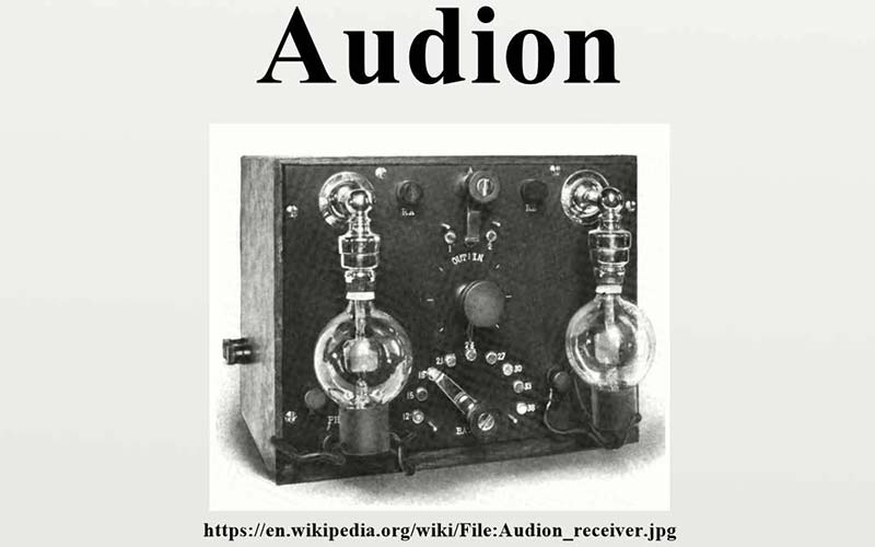
Audion.
Harold Arnold, a young physicist who had just joined AT&T from the University of Chicago, witnessed the demonstration. Unfortunately, the audion had problems. It only worked well at low voltages, not at the higher voltages needed to amplify a telephone current. At higher voltages, it would fill with blue haze and stop working until the current was reduced.
Nonetheless, Arnold was optimistic and convinced that he could develop the audion into a voice repeater. A working group of scientists and engineers was put together to understand and solve the problems. It was through the use of a higher vacuum and an oxide coated filament that they managed to eliminate the problems and improve the tube’s output.
A year later — using Arnold’s thermionic tube — a successful call was made from New York to Baltimore. Then, in 1914, a transcontinental call over 3,400 miles from coast to coast was made.
The unconditional success of this group in developing repeaters for long distance convinced AT&T managers that paying qualified scientists to do research was good business.
The research department of AT&T continued to expand after WWI. In 1925, it was incorporated as a separate entity called Bell Telephone Laboratories with over 3,500 employees. Bell Labs first president was Frank Jewitt, a physicist from the University of Chicago. He picked Arnold as Bell’s first research director.
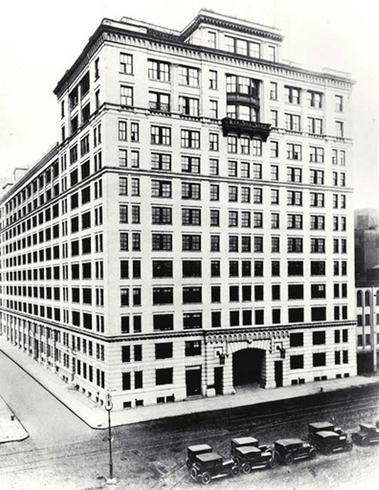
Figure 5. Bell Telephone Laboratories in 1925. This is the West Street building in Manhattan. Image courtesy of AT&T.
Bell Labs Begins Solid-State Research
By the 1930s, physicists began recognizing the important class of substances called semiconductors. Copper oxide and selenium are examples. They are not electrical conductors like metals which have plenty of free electrons to carry current. Neither are they insulators like glass or ceramic, which have very few free electrons and have high electrical resistance. Semiconductors fall between these two groups and have some special properties (as discussed earlier) such as negative temperature coefficient and sensitivity to light.
A major breakthrough in understanding these unusual materials was made by a British theorist, Alan Wilson, who published two papers on The Theory of Electronic Semi-Conductors in 1931. Based on this work, physicists now had a broad quantum mechanical foundation of how electrons behaved in crystals. The focus now shifted to explaining the behavior of actual materials and the opportunity of creating some form of solid-state device.
In 1936, Mervin Kelly — now research director at Bell Labs — decided to establish a department to study solid-state physics in the hope of producing a replacement for the vacuum tube from semiconducting materials. He enlisted a number of people: William Shockley, Russell Ohl, Jack Scaff, and others to begin working on solid-state devices.
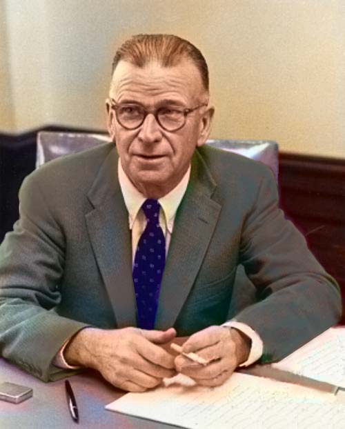
Figure 6. Mervin Joe Kelly was an American physicist and engineer at Bell Labs. His graduate work with R.A. Millikan at the University of Chicago gave him a lasting appreciation of the rarity and importance of first-rate scientists and first-rate research. He did early and important work on vacuum tubes, including research, development, and manufacture. He was Director of Research and ultimately President of Bell Labs in 1951. He formed the research group which developed the transistor, led by William Shockley. Image courtesy of AT&T.
Kelly felt sure that the vacuum tube was not the final answer. He wanted a device that was more reliable, as well as smaller and more efficient. However, just as they were getting started, the group had to disband when World War II broke out, putting the research on hold.
However, a small group at Bell Labs continued solid-state research under the direction of the MIT Radiation Laboratory to purify semiconductor material for the microwave detector used in radar. It was here that Russell Ohl discovered the first P-N junction when he accidentally cut a section of silicon ingot across the boundary between the P and N regions.
From the unusual behavior of the current passing through the sample, he and others concluded that it must be due to “some barrier being formed in the crystal,” but they went no further with it at this time. Wartime research such as this led to a much better understanding of semiconductors such as silicon and germanium.
Postwar Research Resumes at Bell Labs
After the war, Kelly was promoted to vice-president in charge of research. In 1945, he immediately organized research directed at “development of completely new and improved components.” The postwar research efforts were to be in a new laboratory on Murray Hill in New Jersey which was free of noise and vibrations.
William Shockley and physical chemist, Stanley Morgan jointly headed the Solid-State Physics Department. Shockley quickly drafted Bell Lab’s Walter Brattain, an experimental physicist who could build just about anything. Next, he hired a theoretical physicist, John Bardeen, from the University of Minnesota. He then filled out his team with a diverse mix of physicists, chemists, and engineers such as John Pearson, Bert Moore, and Robert Gibney.
This group made a very important decision right at the beginning: that the simplest semiconductors are silicon and germanium; and that their efforts would be directed at understanding them first. They would not waste effort on more complex material such as lead sulfide and copper oxide.
One day, Kelly, Shockley, and others visited Ohl to discuss his research on silicon. First, Ohl briefed them about P-N junctions, the photovoltaic effect, and methods for refining silicon for crystal detectors. He then showed them a radio receiver he had built using point-contact detectors he called “desisters.”
Direct current from a battery flowed through the desister, causing it to amplify the signal. As Shockley recalled, “Ohl demonstrated that amplified radio broadcasts could be heard over a small loudspeaker.” Unfortunately, instabilities made the amplifier erratic and unreliable. Shockley noted 30 years later that “Ohl’s radio set was indeed an exciting solid-state development.”
One must wonder if Ohl was familiar with the work of Losev some years earlier. Indeed, why wasn’t Losev mentioned or referenced in any of the subsequent Bell Labs papers? I’ll leave it to the historians to figure that one out!
In the spring of 1945, Shockley designed what he hoped would be the first semiconductor amplifier, relying on something called "field-effect." His device was a small cylinder coated thinly with silicon, mounted close to a small metal plate. He predicted — based on current theories of germanium and silicon — that when a voltage was applied to the plate, it would cause an increase or decrease in the number of charge carriers in the film, thus regulating the current in it. However, several attempts to fabricate this field-effect device failed.
In October 1945, Shockley asked Bardeen (who had just joined the group) to check the calculations he had made to help account for the failure of his field-effect idea. Two weeks later, Bardeen — taking a different theoretical route — arrived at the same conclusion as Shockley. That no effect was seen was indeed a mystery!
Bardeen now thought that something was preventing the electric field from getting inside the semiconductor surface. He discussed this with Shockley who encouraged him to continue research.
A few months later in 1946, Bardeen had an answer based on a creative model of “surface states.” In this model, electrons drawn to the semiconductor surface become trapped in localized states and are unable to act as charge carriers. These states effectively shield the semiconductor from the voltage of the control plate. Was this theory real? This question became intensely interesting to the group.
Inventing the Point-Contact Transistor
In the following months, the Bell Labs group responded to Bardeen’s surface state idea with an intensive research program. With a broad range of talents, the group worked extremely well together. Brattain describes this period in glowing terms saying there was much rapport in the group.
Bardeen worked closely with Brattain and Pearson. In November 1947, Brattain made an important discovery based on a suggestion of Gibney. He found that he could neutralize the effect of the surface states by immersing the silicon in an electrolyte. “This new finding was electrifying,” observed Shockley, adding that “at long last, Brattain and Gibney had overcome the blocking effect.”
This discovery set in motion work that culminated one month later in the first transistor.
Through a series of experiments, Bardeen and Brattain tried to use the discovery to build a field-effect amplifier. One bizarre suggestion by Bardeen involved freezing a thin film of germanium with liquid nitrogen to “freeze” the surface electrons in place. Applying 500 volts, they found only a tenth of one percent change in its conductivity. However, Bardeen was convinced that they were seeing the field-effect that Shockley had predicted.
They began using a point contact pressed against a specially prepared silicon surface with an N-type “inversion layer.” They used a drop of electrolyte on the surface as one contact and the metal point as the other. They obtained small but significant power amplification, but very poor frequency response. Meeting for lunch Bardeen, Brattain, and Shockley discussed how to overcome this problem.
In an attempt to improve the frequency response, Brattain evaporated a gold plate onto a thin oxide layer on a germanium slab with an inversion layer. He thought the oxide would insulate the gold from the germanium, but unknown to him it had somehow been washed away leaving the gold in direct contact. They were surprised to find that they could still modulate the voltage and current.
This serendipitous event pointed them in a different direction. Bardeen realized that a new and different phenomenon was occurring at the interface between the gold and germanium.
After talking the problem over, they decided that they needed to put two point contacts on the surface close together. Brattain found a way to form a narrow gap without wires as shown in Figure 7. He used a plastic wedge with a strip of gold foil cemented around the edge. He cut the foil with a razor forming a very thin gap.
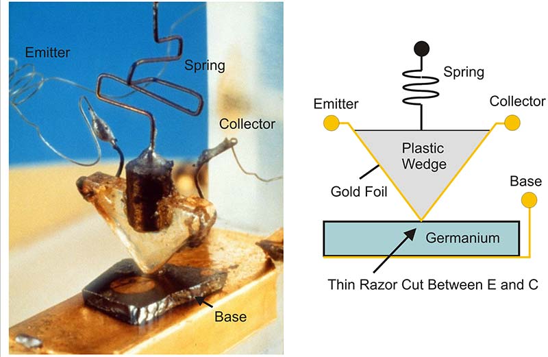
FIGURE 7. First point-contact transistor is on left. On the right is the schematic representation. Image courtesy of AT&T.
On December 16, 1947, they tested the new device and obtained a 30 percent power gain and voltage gain of 15 on a 1,000 Hz input signal. The transistor amplifier was born! A week later, on December 23, 1947, it was demonstrated to Bell Labs executives in a circuit that produced amplified speech in headphones.
From Point Contacts to the Junction Transistor
During much of this work, Shockley had been away in Europe on a short sabbatical but returned around Christmas time and was chagrined to find that he was not part of the invention. For weeks afterwards, Shockley had mixed emotions.
He was elated with the group’s results but bothered that he did not have a direct role in the breakthrough. He was also upset that his own field-effect idea was being overlooked, which he thought had been the crucial spark that led to the invention.
He was puzzled by the fact that the “transistor principle” was not clear as well. For example, the slightly over unity current gain and the occasional negative resistance behavior could not be explained. He was deeply skeptical of Bardeen’s explanation of how electrons and holes flowed in their semiconductor. In any case, the invention spurred him into action.
Soon thereafter, during a meeting of the Physical Society in Chicago on New Year’s Eve in 1947, he began formulating his own unique approach to a semiconductor amplifier. Three weeks later, on January 23, 1948, he conceived the design with a three-layer semiconductor structure. There were no unwieldy point contacts. Two P-N junctions at the interfaces served in their place. He had worked out the process of carrier injection in germanium!
His device was more rugged and more practical than the point-contact transistor, and much easier to manufacture. Shockley’s achievement is truly amazing since the theory of the junction transistor was developed before it was made.
Another month passed before Shockley revealed his breakthrough idea to the group. Why did he keep the information to himself? Did he need to keep quiet to follow up on its theoretical and practical implications? Or, was there some other reason? We do not know.
On February 26, 1948, the company applied for four patents on semiconductor amplifiers, including Bardeen and Brattain’s original application on the point-contact transistor. One day later, Bell applied for Shockley’s patent on the junction transistor. It was John Pierce — combining the words “trans-resistance” — who coined the name “transistor.”
On June 30, 1948, Bell announced the invention of the point-contact transistor in a press conference. The invention got little attention at the time, either in the popular press or in industry.
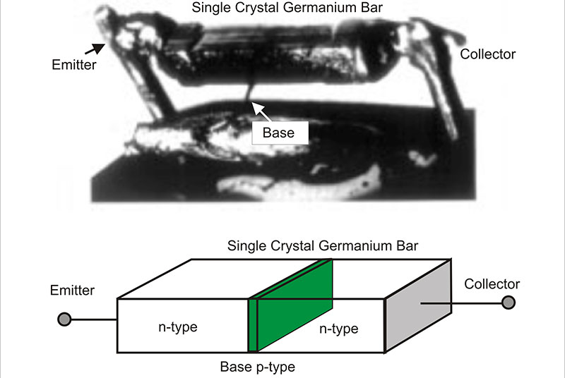
Figure 8. First junction transistor is above. Below is the junction arrangement in the germanium bar. The base layer is only one to two mils thick. Image courtesy of AT&T.
Western Electric ushered the point-contact transistor into production in 1951. It saw service in the switching gear used for making long distance dialing. It didn’t succeed in the commercial marketplace, however, except in niche usage in hearing aids and military equipment.
Over time, it became clear that the point-contact theory described in the Bell patents was incomplete. It was Shockley — with his work on P-N junctions and transistor theory — who put solid-state physics on a solid foundation. Much of this research is discussed in his book, Electrons and Holes in Semiconductors, published in 1950, which became the bible of solid-state.
In late 1949, Teal — working with Sparks and Morgan — developed a method for pulling single crystals out of molten germanium. This allowed them to dope the germanium in a controlled manner to fabricate the first practical N-P-N transistor. On the date of its demonstration — April 20, 1950 — Shockley wrote in his notebook, “An N-P-N unit was demonstrated today.” The future now belonged to the junction transistor.
Epilog
The events of 1948 had caused a rift in Bell’s semiconductor group. Bardeen and Brattain with their point-contact device were on one side and Shockley and his assistants working on the junction device were on the other. A once cooperative environment was turned into one that was highly competitive. The questions of whose names should be on the patent for the device and who should be featured in publicity photographs sent tensions higher still.
Bardeen became unhappy with the Bell situation and began working on another mystery: superconductivity. Unfortunately, his research was not going well. There were few others at the lab interested in the problem and no experimental work was going on.
Bardeen eventually left Bell in 1951 for the University of Illinois, where he continued work on superconductivity. In 1957, he wrote a seminal paper, Theory of Superconductivity which ranks as one of the pivotal contributions in physics. Recognizing its great importance, the Swedish Academy awarded him a second Nobel Prize in 1972.
Brattain stayed on at Bell Labs doing research for several years and becoming an ambassador of good will. After retirement in 1967, he moved to Whitman College in Walla Walla, Washington. There, he spent the rest of his life at the college working on biophysics and teaching undergraduate physics courses.
Shockley saw the potential in the transistor. He left Bell Labs in 1955 and founded Shockley Semiconductor in Palo Alto, California, hiring the best engineers and physicists. He was eventually eased out of his directorship by other managers who were tired of owning a company led by a headstrong physicist.
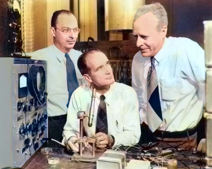
Figure 9. Shown here from left are John Bardeen, William Shockley, and Walter Brattain at Bell Labs in 1948 with apparatus that led to the invention of the transistor. Image courtesy of AT&T.
It’s interesting to note that Shockley's company and the engineers and physicists whom he brought to California were the beginning of Silicon Valley. After Shockley left the directorship, he was grabbed up by Stanford’s Frederick Terman, as Professor of Engineering and Applied Science. He also returned to Bell labs as an executive consultant.
On December 10, 1956, Shockley, Bardeen, and Brattain (in that order) were awarded the Nobel Prize in physics for their ‘‘investigations on semi-conductors and the discovery of the transistor effect.’’ After they received their awards, there was a celebration that night at the Grand Hotel. At a table in the dining room, the three men and their spouses seemed to forget the bruises and wounds of the past amid the warm glow of champagne and the glory of the moment.
The physical insights of these three very different men were what made possible the invention of the transistor. The three inventors could hardly have known the outcome when they made their discovery in 1947: That they were going to change the world. NV
REFERENCES
[1] Bo Lojek, “History of Semiconductor Engineering,” Springer, 2007.
[2] P. R. Morris, “History of the World Semiconductor Industry,” The Institution of Engineering and Technology, 2008.
[3] Michael Riordan, Lillian Hoddeson, “Crystal Fire,” W. W. Norton & Company, 1997.