SAFETY REMINDER
When building the boost power supply, remember that — depending on the components chosen in the design — high voltages can be generated. Care should be exercised to avoid electrical shock. Capacitors can hold energy after the power is removed from the circuit.
In Part 1, we covered the theory of how a boost power supply works. We introduced pulse width modulation (PWM) and explained how to get the 18F2455 PIC to output a square wave with a given period and duty factor. We covered the important parameters in designing the boost power supply and used the free LTSPICE program to come up with a possible design.
Now, we will build the power supply designed last time on a printed circuit board. We will write the software needed to drive the PIC in a freely downloadable version of the C language. We will discuss the software that drives the A/D conversion, the LCD display, and the pulse width modulation. Then, we will program the microprocessor with the software. I will mention some of the pitfalls in designing a switching power supply and, finally, test the power supply.
Circuit Construction
The boost power supply can easily be built on a breadboard or printed circuit board (PCB). Figure 1 is the schematic for the actual circuit that was built. Several components were added to the circuit from the basic design in Part 1. The first of these is the 18F2455 microprocessor that was modeled as a square wave generator in Part 1. In this circuit, the PWM output pin RC2 (pin 13 on the PIC18F2455) is used to drive the MOSFET that charges and discharges the inductor.

FIGURE 1. Boost power supply schematic.
The PIC18F2455 can control an LCD display, so an optional LCD display was added along with the R9 potentiometer that is the LCD’s contrast control. The LED D3 was added to flash periodically as an indicator that the PIC18F2455 is programmed and operating properly. The R10 potentiometer was added to allow a user to fine tune the LCD’s display of output voltage to match the actual output voltage.
The R1 potentiometer was added to allow the user to set the desired output voltage. The microprocessor will attempt to maintain this output level by changing the ON time of the PWM. The output voltage at test point #1 is fed to the analog-to-digital converter point RA0 (pin 2 on PIC18F2455), where it is converted to a digital value. This digital value is compared to the desired output voltage, and the difference is used to increase or decrease the ON time of the PWM.
The programming connector — T4 — and its associated components, were added to allow the 18F2455 PIC to be reprogrammed without removing it from the circuit. The USB connector — T5 — was added to allow for experimentation using the USB as a five-volt power source.
The diode — MBRS3201T3 — is a 200-volt, three-amp Schotty diode that has a very low forward-voltage drop for an ultrafast rectifier. This means it offers very little resistance to the flow of current in one direction. The MBRS3201T3 is only available in a surface mount package.
After initial debugging, the boost power supply was built on a one-sided, 3 inch x 4.5 inch PCB using the pattern shown in Figure 2. The traces shown in red are component-side jumper wires.
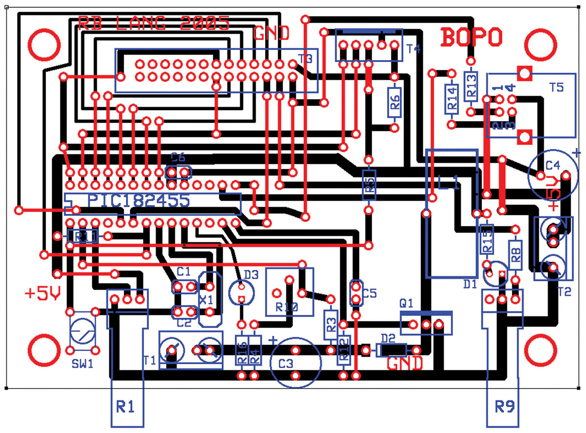
FIGURE 2. PCB layout showing jumper wires.
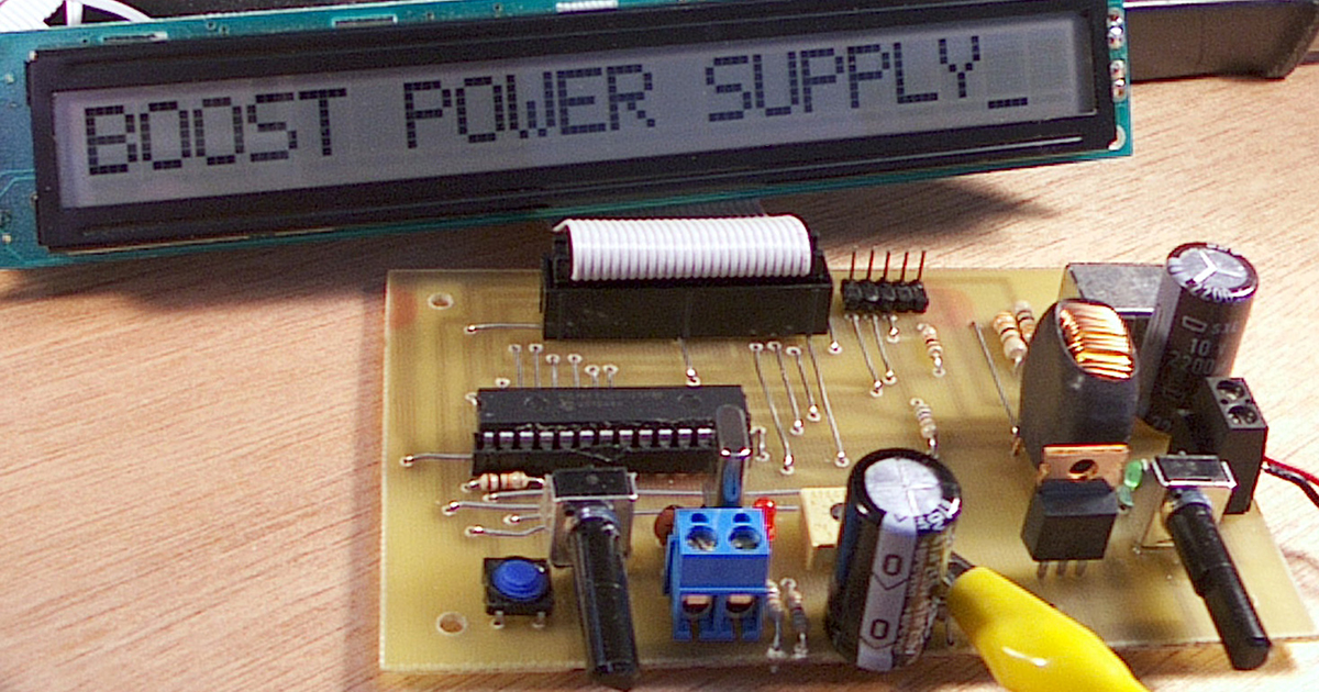
The completed circuit board is shown in Figure 3.
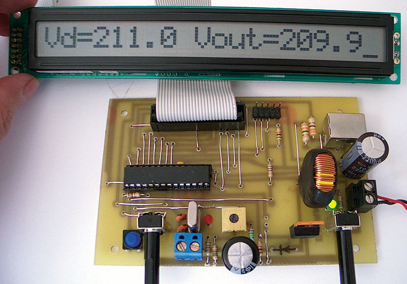
FIGURE 3. Completed boost power supply on circuit board.
Here are the steps for building this board:
Step 1: Solder all jumpers first, since some are beneath components that will be added later.
Step 2: Solder the surface mount diode — D2 — to the copper side of the PCB.
Step 3: Solder all resistors and the R10 potentiometer.
Step 4: Solder the sockets, T1-T6.
Step 5: Solder all capacitors.
Step 6: Solder remaining components.
Step 7: Plug the LCD into the T3 connector.
Vin is +5 volts DC. I added a USB port to the boost power supply, since +5 volts DC can be obtained directly from the USB port, eliminating the need for a five-volt DC power supply. The boost power supply requires about 250 milliamps at five volts to drive the output load at 200 volts and 2.5 milliamps. You should test your application’s current requirements before powering from the USB port, since the USB port has a limit of one amp and might not be protected from overload.
When building the boost power supply, one tool that is very handy to have is an inductance/capacitance meter. Figure 4 shows one such meter measuring a 606 microhenry inductor.
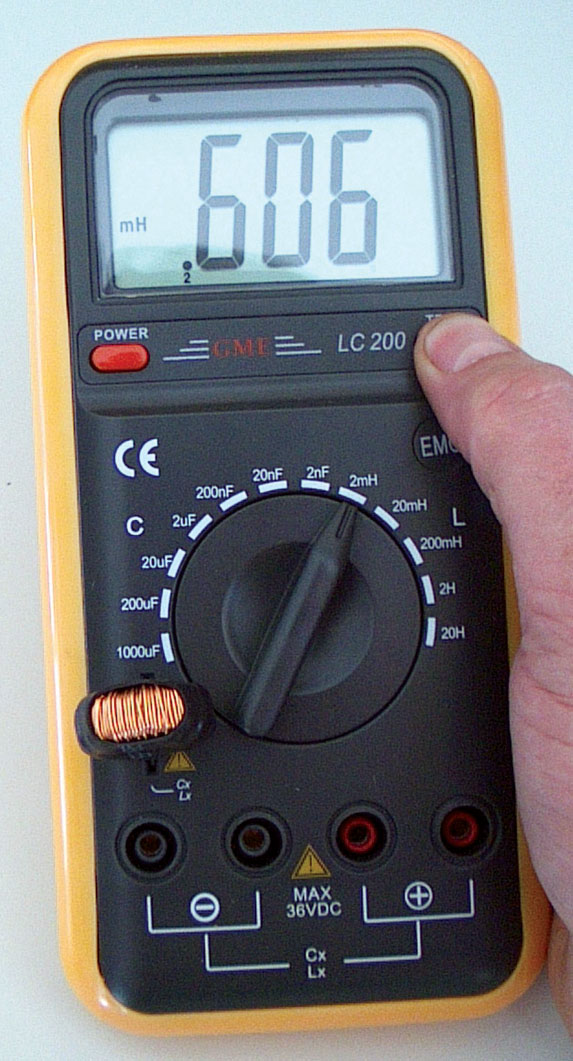
FIGURE 4. Using an inductance-capacitance (LC) meter to measure an inductor.
This meter — which costs about $50 — is useful for identifying the value of poorly marked inductors or capacitors.
Software Development
Using the free, C18 student edition C compiler, I wrote a program for the microprocessor to control switching the MOSFET. This free compiler is/was available (see References) and integrates flawlessly into the MPLAB integrated development environment (see References again.)
The C18 compiler also includes libraries of functions that can be linked directly into your application using the MPLINK linker. These libraries provide simplified control of hardware peripherals such as analog-to-digital converters, pulse width modulation, and timers.
In addition, the libraries provide 32-bit, floating-point math and trig functions, memory and string formatting functions, and character output functions. I made use of these functions to keep the C program short and concise.
My initial plan was to use the floating-point math and output functions in the C18 library, but I found that C18 had no function to format floating-point for output. I also found that by limiting my math to integers, I could reduce the program size by 2,456 bytes in a 9,537 byte program. Thus, to reduce program size, all calculations use integer math.
The optional liquid crystal display (LCD) shown in the Parts List uses the Samsung KS0066 (S6A0069) controller. The C18 library routines were written for the Hitachi HD44780 LCD controller, so I modified them to work with the Samsung controller. These modified routines are included in the C18 source code.
The program consists of two parts. The MAIN program initializes the microprocessor and displays the information on the LCD. The interrupt routine handles the analog-to-digital (A/D) conversion of the desired and actual voltages, does the voltage comparisons, calculates the correction factors, and adjusts the PWM duty cycle. The desired voltage is input from an A/D of a potentiometer on pin RA1. The measured voltage is from the A/D converter on pin RA0.
I used a resistor divider network to scale the output voltage to 0-5 volts. At an output voltage of 100 volts, the voltage across the 8 kΩ resistor combination (R4 and R10) is 2.37 volts, or 484 counts after digital conversion. Full scale on the A/D conversion is 1023/484*100, or 211 volts. I used this information to scale the VDES and VOUT readings to 0-211 volts. The R10 potentiometer can be adjusted so the combined resistance of R10 and R4 will cause the LCD to read VOUT=100.0 when the actual output is 100 volts.
Software Description
Main — The main program calls ADCInit() to initialize the analog-to-digital conversion, EnableInterrupts() to initialize timer and PWM functions, and LCDInit() to initialize the LCD. The program then goes into an infinite loop erasing the LCD, displaying voltages, erasing the LCD, displaying ON time in nanoseconds, erasing the LCD, and displaying the period in nanoseconds. Delays are inserted to allow time for the display to be read.
Key program constants are defined in common program memory: PERIOD=32000 is the period in nanoseconds of the PWM square wave. This value can range from 1-338,640 nanoseconds. MAXVOLTS=211 is the maximum output voltage of the power supply. This is determined by the values of R3, R4, and R10. PERIOD_TIME_UNIT=1332 is the time in nanoseconds, corresponding to one unit in the period (PR2) register and is equal to TOSC (20.8 ns) * TIMER2 prescaler (16) * 4 ~= 1332 ns.
EnableInterrupts() — This routine sets up and enables Timer0 for the timer interrupt. Timer2 is started since it is needed for the PWM function. OpenPWM1() is called to start the PWM function with the proper period.
ONTIME() — This routine calculates the voltage error from VDES-VOUT. The variable On_Time, is increased if the error is positive and decreased if the error is negative. On_Time is kept within a valid range for the PWM input. On_Time is a shared common value.
ADCInit() — This routine calls the OpenADC() library function to set up the A/D conversion on pins RA0 and RA1. This routine also sets up other PORTA pins as digital for use as control lines for LCD display.
ADCGet() — This routine will select RA0 and then RA1 for A/D conversion. It waits until the conversions are complete, then stores the values in variables VDES and VOUT. Values are 0-1,023 counts.
SendLCDCommand() — This will set up control lines and send a one-byte command to the LCD display.
SendLCDData() — This will set up control lines and send one byte of data to the LCD display.
WaitWhileBusy() — This routine will wait until the busy bit, RB7, is cleared by the LCD. The busy bit is checked once every five milliseconds.
LCDErase() — This routine will send the erase command, 0x01, to the LCD. The busy bit is checked before and after the command is sent.
LCD_Display_Rom() — This routine will display a string stored in program (ROM) memory.
LCD_Display_Ram() — This routine will display a string stored in data (RAM) memory.
LCDInit() — The LCDInit() routine initializes the LCD display. Commands are sent to put the display in auto increment mode and turn the cursor on and the blinking off. The LCD is erased by calling the LCDErase() routine. A message “BOOST POWER SUPPLY” stored in program memory is displayed by a call to LCD_Display_Rom. Appropriate delays are used until the LCD busy bit is available.
DisplayVoltages() — The Display Voltages() routine scales the VDES and VOUT counts from the A/D converter to 0.0-211.0 volts DC for display. All calculations use integer arithmetic to decrease the size of the program. Integer volts and tenths of volts are stored in separate variables. The sprintf() function from the C18 library is used to format a string for display, and the LCD_Display_Ram() function is used to output the string to the LCD.
DisplayONTIME() — This routine will display the value of the ON time. On_Time is converted to nanoseconds and displayed on the LCD using the sprintf() and LCD_ LCD_Display_Ram() functions.
DisplayPeriod() — This routine will display the period in nanoseconds on the LCD using the sprintf()and LCD_Display_Ram() functions.
Timer_handler() — Timer_handler() is the interrupt routine that is called every 1,000 microseconds when Timer0 overflows. This routine performs the A/D conversion by calling ADCGET(), calculates a new On_Time by calling subroutine ONTIME(), and modifies the PWM duty cycle by calling the C18 library function SetDCPWM1() with On_Time as the argument. The Timer0 interrupt flag is cleared and the timer is reloaded by a call to the C18 library function WriteTimer0().
Programming the Microprocessor
The C compiler is used to compile and link the C source into the bopo.hex file. The next step in the process is to download the hex file to the PIC18F2455 chip. For this, you will need PIC programmer hardware and PIC programmer software for the PC. The PIC programmer’s connector plugs into the T4 connector in Figure 1.
There are lots of schematics for PIC programmers and free PIC programmer software on the Internet. I like the TAIT programmer hardware. It uses the PC’s parallel port and the PIPVb programming software shown in Figure 5.
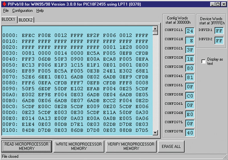
FIGURE 5. PIC programming software.
Just make sure the programming software is tested on the operating system you are using and works for the PIC18F2455 since the programming algorithm was changed by Microchip for this PIC (see References).
Switching Power Supply Pitfalls
There are many factors that need to be considered when designing a boost power supply. One of the most important considerations is the layout of the PCB. The following suggestions are taken from Reference 5:
- Use a low electro-magnetic interference (EMI) inductor with a ferrite type closed core. Examples include toroid and encased E core inductors.
- Run the feedback trace as far from the inductor and noisy power supply traces as possible.
- Locate a low value ceramic input filter capacitor as close to the Vin pin of the IC as possible.
- Make sure all power traces are as short, direct, and thick as possible. Size PCB traces for maximum current to be carried — at least 15 millimeters per amp.
- Keep the inductor, output capacitor, and output diode as close to each other as possible. This will help to reduce EMI radiated by the power trace.
- Arrange components so that the switching current loops curl in the same direction. This will prevent magnetic field reversal caused by the traces between the two half-cycles and reduce radiating EMI.
- Use the copper area on the PCB as a heatsink for components, if possible.
- Use a ground plane for the control circuit. Try to make the connections to the ground plane through vias rather than through PCB traces.
Sample Applications
Now that we have completed our boost power supply, let’s use it to power an application. There are several applications we might use the boost power supply for. We could use it as a 13-volt, DC power supply to supply programming voltage for a USB PIC programmer (see References). Or, we could supply 170 volts DC at 2.5-4 mA to drive a Nixie tube (see References). Nixie tubes are the precursors to the alphanumeric LEDs of today. They are no longer manufactured in the USA, but they can be found on eBay from sources in Russia and the Ukraine. Figure 6 shows additional circuitry necessary to drive a Nixie tube.
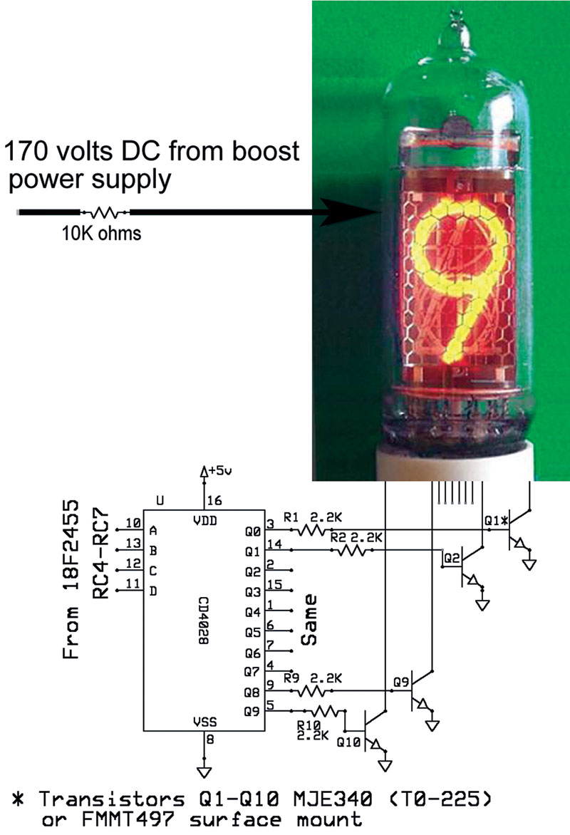
FIGURE 6. Nixie tube driver circuit.
We will do a simple application involving neon lamps. The NE-2 is a cold-cathode neon gas discharge tube meant for use as an indicator light. It has two parallel electrodes sealed in a small glass envelope with neon gas. The discharge will start at about 65 volts, and the more current that flows, the more the orange discharge will cover the negative electrode. It only requires a few tenths of a milliamp to give full glow. For this reason, a current limiting device — like a resistor — is used.
The glow lamp cannot only be used as an indicator, but also as a useful circuit element. Figure 7 shows a simple circuit that can be connected to the boost power supply that will flash two neon bulbs alternately.

FIGURE 7. Neon flasher circuit.
Smaller values of the capacitors and resistors increase the flashing frequency, larger values slow the flasher down. The higher the voltage, the faster the lights will alternately flash. The capacitor should be non-polarized with a voltage rating of more than 100 volts. Figure 8 shows the working neon flasher hooked up to the boost power supply.
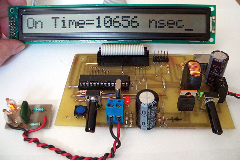
FIGURE 8. Working neon flasher.
With the simple flasher circuit, we have the start of an oscillator. In the past, the tremolo circuit in the classic Fender guitar amplifier used a neon lamp and a CdS photocell.
Conclusion
We have now completed construction of the boost power supply that was designed in Part 1. We developed the C software needed to drive the PIC. We discussed how the software handles the A/D conversion, the LCD display, and the PWM. We programmed the microprocessor with the software. We discussed some of the pitfalls in designing a switching power supply and, finally, used the power supply to power some applications. NV
PARTS LIST FOR BOOST POWER SUPPLY
| Qty |
Part ID |
Description |
Source/Ref Part No. |
| 2 |
T1, T2 |
Two screw terminals |
1 / 164793 |
| 1 |
T3 |
26-pin socket |
1 / 68371 |
| 1 |
T4 |
Programming connector |
1 / 153699 |
| 1 |
T5 |
USB PCB connector |
1 / 230957 |
| 1 |
T6 |
Two pin socket for crystal |
1 / 167003 |
| 1 |
PCB |
Printed circuit board kit |
1 / 70412 |
| 1 |
SW |
Reset switch (momentary contact) |
1 / 122972 |
| 1 |
X1 |
20 MHz crystal |
1 / 14517 |
| 2 |
C1, C2 |
22 pF disk capacitor |
1 / 15405 |
| 1 |
C5 |
470 nF electrolytic capacitor |
1 / 25558 |
| 1 |
C3 |
47 µF electrolytic capacitor, 250 V |
1 / 330616 |
| 1 |
C4 |
2200 µF electrolytic capacitor, 16 V |
1 / 133146 |
| 1 |
C6 |
0.1 µF |
1 / 25523 |
| 2 |
R1, R9 |
10K potentiometer |
1 / 241453 |
| 5 |
R2, R6, R7, R11, R12 |
10K resistor |
1 / 29911 |
| 1 |
R3 |
330K ohm resistor |
1 / 30883 |
| 1 |
R4 |
5.6K ohm resistor |
1 / 31270 |
| 4 |
R5, R8, R15, R16 |
560 Ω resistor |
1 / 31376 |
| 1 |
R10 |
5K potentiometer |
1 / 43078 |
| 2 |
R13, R14 |
27 Ω resistor [1]* |
1 / 30584 |
| 1 |
D1, D3 |
LED |
1 / 206498 |
| 1 |
LCD1 |
Optional 20-character LCD |
2 / 8087 |
| 1 |
D2 |
MBRS3201T3 |
3 |
| 1 |
IC1 |
Blank PIC18F2455, microprocessor, Preprogrammed chip |
5, 8 |
| 1 |
Q1 |
IRF730 MOSFET |
1 / 210551 |
| 1 |
L1 |
220 µH, 3.6 A inductor |
1 / 371418 |
| *[1] All resistors 1/4 watt |
Downloads
High Voltage PIC 2006-10 (PCB Layout showing the jumper wires)