The first two parts in this series explained modern TTL and CMOS logic gate basics and gave practical descriptions of some of the most popular digital buffer, inverter, and AND gate logic ICs that are available. This time, we’ll expand on this basic theme and talk about a variety of popular NAND gate and OR gate ICs that are available from either your local supplier or from specialist dealers.
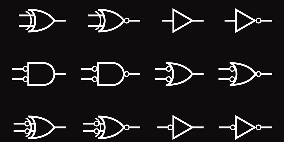
Practical NAND-Gate Digital IC Circuits
The output of a digital NAND gate goes low when all of its inputs (A and B, etc.) are high. Figure 1 lists basic details of 13 popular NAND-gate ICs.
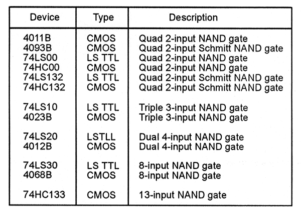
FIGURE 1. Thirteen popular NAND gate ICs.
Of these, the 74LS00, 74HC00, and 4011B (see Figures 2 and 3) are standard quad two-input types.
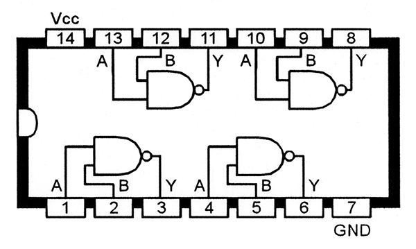
FIGURE 2. Functional diagram of the 74LS00 or 74HC00 quad two-input NAND gate IC.
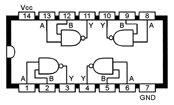
FIGURE 3. Functional diagram of the 4011B quad two-input NAND gate IC.
The 4093B, 74LS132, and 74HC132 (see Figures 4 and 5) are Schmitt quad two-input types.
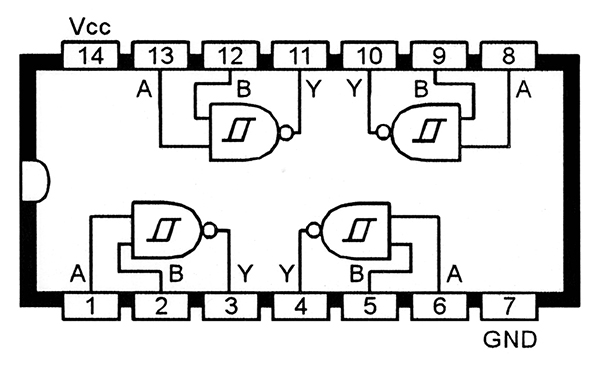
FIGURE 4. Functional diagram of the 4093B quad two-input Schmitt NAND gate IC.
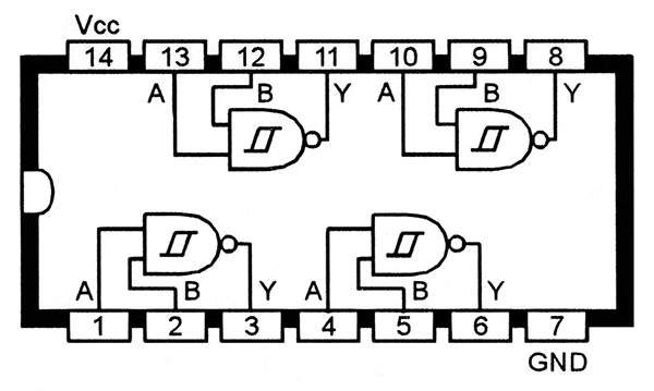
FIGURE 5. Functional diagram of the 74LS132 or 74HC132 quad two-input Schmitt NAND gate ICs.
The 74LS10 and 4023B (see Figures 6 and 7) are triple three-input standard types.
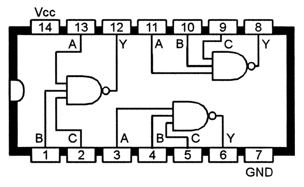
FIGURE 6. Functional diagram of the 74LS10 triple three-input NAND gate IC.
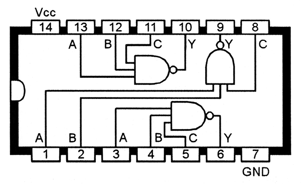
FIGURE 7. Functional diagram of the 4023B triple three-input NAND gate IC.
The 74LS20 and 4012B (see Figures 8 and 9) are dual four-input standard types.
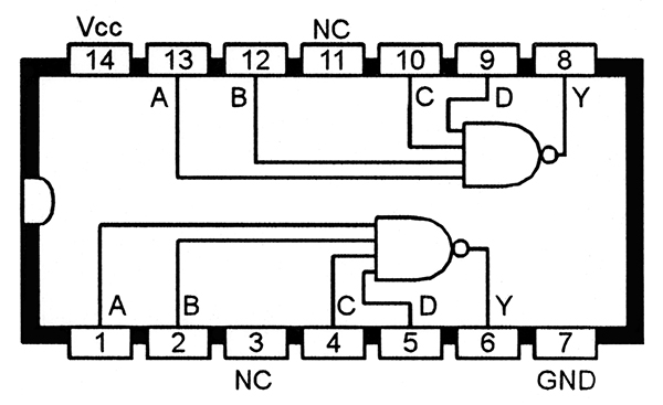
FIGURE 8. Functional diagram of the 74LS20 dual four-input NAND gate IC.
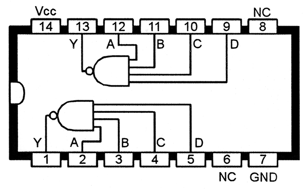
FIGURE 9. Functional diagram of the 4012B dual four-input NAND gate IC.
The 74LS30 and 4068B (see Figures 10 and 11) are eight-input standard types; and the 74HC133 is a 13-input standard type.
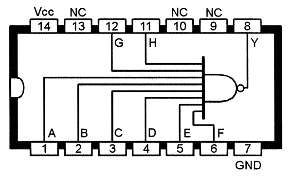
FIGURE 10. Functional diagram of the 74LS30 eight-input NAND gate IC.
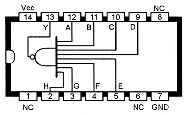
FIGURE 11. Functional diagram of the 4068B eight-input NAND gate IC.
When using NAND gate ICs, each unwanted gate should be disabled by shorting all inputs together and tying them to one of the IC’s supply lines. In CMOS ICs, the shorted inputs can be wired directly to either supply line, but in TTL ICs the inputs must (to give minimum quiescent current consumption with good stability) be tied directly to the 0V rail, as shown in Figure 12.
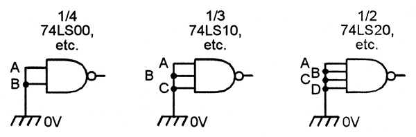
FIGURE 12. Methods of disabling unwanted TTL NAND gates.
Sometimes, when using NAND gate ICs, you may not want to use all of a gate’s input terminals. In this case, the unwanted inputs can be disabled by either tying them high (directly in CMOS gates, or via a 1K resistor in TTL types) or by simply shorting them directly to a used input. Figure 13 shows examples of a three-input TTL NAND gate wired for use as a two-input type.
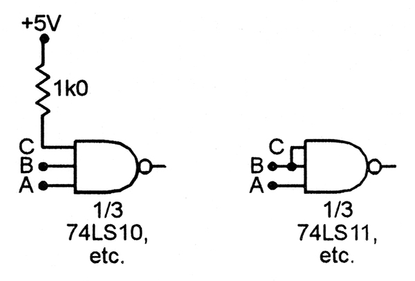
FIGURE 13. Basic method of disabling unwanted TTL NAND gate inputs.
Note that the fan-in of a TTL NAND gate is an almost constant ‘1,’ irrespective of the number of inputs used. Thus, CMOS or TTL NAND gates can be converted into simple inverters by simply shorting all of their inputs together. Figure 14 shows examples of TTL NAND gates used as inverters.
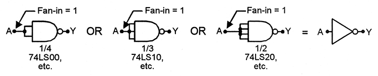
FIGURE 14. Methods of using TTL NAND gates as simple inverters.
Also note that NAND gates are fairly versatile elements, as demonstrated in Figure 15, which shows ways of using two-input elements to make a two-input or three-input AND gate or a three-input NAND gate.

FIGURE 15. Ways of using two-input NAND gates to make various AND and NAND gates.
Practical OR Gate IC Circuits
The output of an OR gate goes high when any of its inputs (A or B, etc.) go high. The simplest way to make an OR gate is via a number of diodes and a single resistor, as shown (for example) in the three-input OR gate of Figure 16.

FIGURE 16. Simple three input diode OR gate.
The diode OR gate is reasonably fast, very cost-effective, and can readily be expanded to accept any number of inputs by simply adding one more diode to the circuit for each new input.
Relatively few dedicated OR gate ICs are available. Figure 17 lists basic details of the six most popular OR gate ICs.
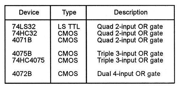
FIGURE 17. Six popular OR gate ICs.
The 74LS32, 74HC32, and 4071B (see Figures 18 and 19) are quad two-input types.
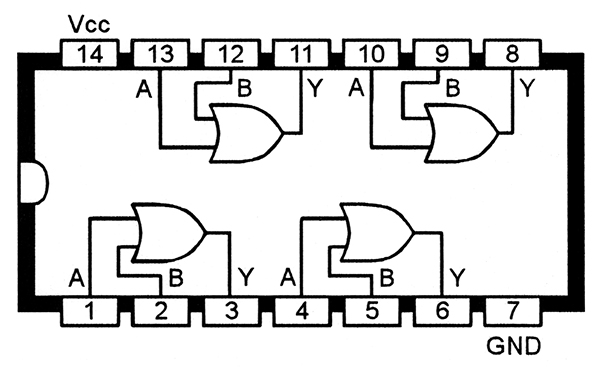
FIGURE 18. Functional diagram of the 74LS32 or 74HC32 quad two-input OR gate IC.
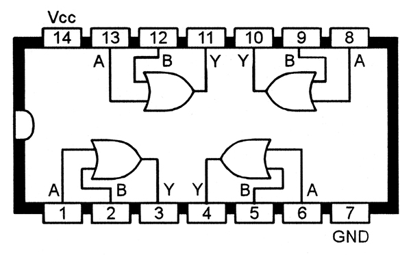
FIGURE 19. Functional diagram of the 4071B quad two-input OR gate IC.
The 4075B and 74HC4075 (see Figure 20) are triple three-input types.
FIGURE 20. Functional diagram of the 4075B or 74HC4075 triple three-input OR gate IC.
The 4072B (see Figure 21) is a dual four-input type.
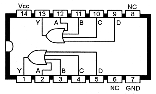
FIGURE 21. Functional diagram of the 4072B dual four-input OR gate IC.
When using OR gate ICs, each unwanted gate should be disabled by shorting all of its inputs together and tying them to one of the IC’s supply lines. In CMOS ICs, the shorted inputs can be wired directly to either supply line, but in TTL ICs the inputs must (to give minimum quiescent current consumption with good stablity) be tied high via a 1K resistor, as shown in Figure 22.
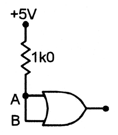
FIGURE 22. Method of disabling a TTL OR gate.
Note that the fan-in of a TTL NOR gate is directly proportional to the number of inputs used — at a fan-in rate of one per input — and that a TTL two-input OR gate can be made to act as a simple non-inverting buffer by either tying one input to ground or by tying both inputs together, as shown in Figure 23.
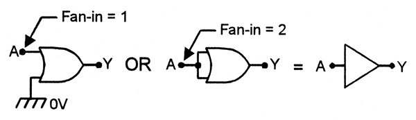
FIGURE 23. Ways of using a TTL OR gate as a simple buffer.
Just make sure the buffer has a fan-in of one in the former case, and a fan-in of two in the latter. Also note that OR gates can be directly cascaded to make a compound OR gate with any desired number of inputs. Figure 24, for example, shows ways of cascading two-input elements to make OR gates with three, four, or five inputs.

FIGURE 24. Ways of cascading two-input OR gates to get up to five inputs.
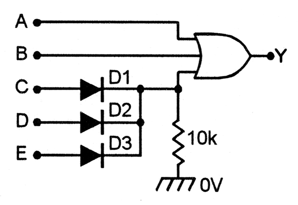
FIGURE 25. Example of a compound five-input OR gate circuit.
Figure 25 shows a three-input OR element and a three-input diode OR gate cascaded to make a compound five-input OR gate. NV