The first three installments of this five-part series explained modern TTL and CMOS logic gate basics and gave practical descriptions of some of the most popular digital buffer, inverter, AND gate, NAND gate, and OR gate digital ICs that are available. This time, we expand on this theme and describe a variety of popular NOR gate, EX-OR gate, and EX-NOR gate ICs that are available from either your local supplier or from specialist dealers.
Practical NOR-Gate Digital IC Circuits
The output of a digital NOR gate goes low when any of its inputs (A or B, etc.) go high. One easy way to make a NOR gate is to combine a basic diode OR gate with a transistor or IC inverter stage, as shown in the three-input NOR gate circuits of Figures 1(a) and 1(b)

FIGURE 1. A simple NOR gate can be made by feeding the output of a diode OR gate through a transistor or IC inverter stage.
NOR gates of this type are reasonably fast and cost-effective and can easily be expanded to accept any desired number of inputs by simply adding one new diode for each new input. Figure 2 lists basic details of the 10 most popular NOR gate ICs.
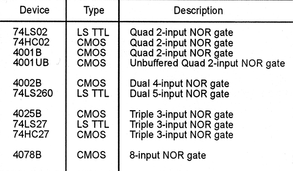
FIGURE 2. Ten popular NOR gate ICs.
Of these, the 74LS02, 74HC02, 4001B, and the unbuffered 4011B (see Figures 3 and 4) are all Quad two-input types.
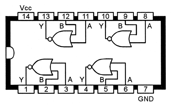
FIGURE 3. Functional diagram of the 74LS02 or 74HC02 Quad two-input NOR gate IC.
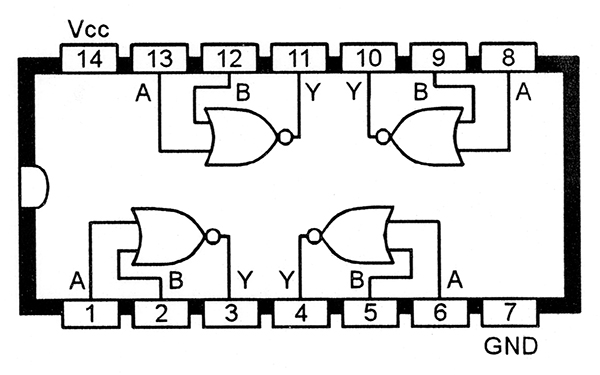
FIGURE 4. Functional diagram of the 4001B or 4001UB Quad two-input NOR gate IC.
The 4025B and the 74LS27 and 74HC27 (see Figures 5 and 6) are Triple three-input types.
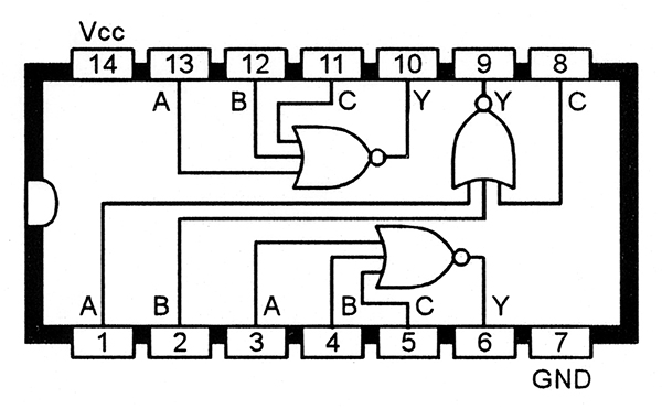
FIGURE 5. Functional diagram of the 4025B Triple three-input NOR gate IC.
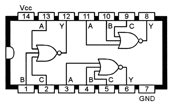
FIGURE 6. Functional diagram of the 74LS27 or 74HC27 Triple three-input NOR gate IC.
The 4002B and 74LS260 (see Figures 7 and 8) are Dual four-input and five-input types, respectively.
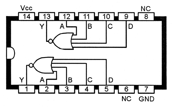
FIGURE 7. Functional diagram of the 4002B Dual four-input NOR gate IC.
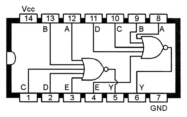
FIGURE 8. Functional diagram of the 74LS260 Dual five-input NOR gate IC.
The 4078B (Figure 9) is an eight-input NOR gate IC.
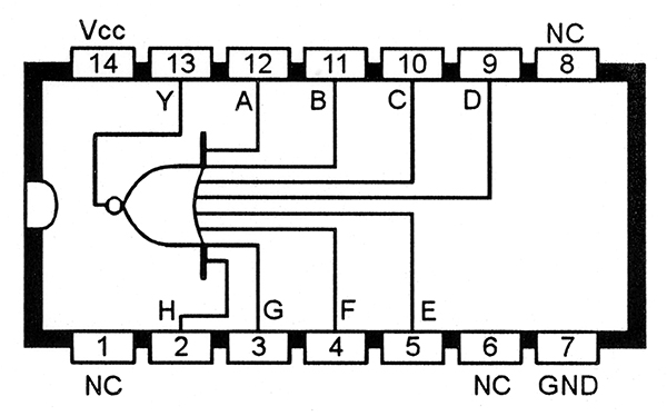
FIGURE 9. Functional diagram of the 4078B Dual eight-input NOR gate IC.
When using NOR gate ICs, each unwanted gate should be disabled by shorting all of its inputs together and tying them to one of the IC’s supply lines. In CMOS ICs, the shorted inputs can be wired directly to either supply line, but in TTL ICs the inputs must (to give minimum quiescent current consumption with good stability) be tied directly to the ground rail, as shown in Figure 10.

FIGURE 10. Ways of disabling TTL NOR gates.
Sometimes when using NOR gate ICs, you may not want to use all of a gate’s input terminals. In this case, the unwanted inputs are best disabled by shorting them directly to ground, as shown in the examples of Figure 11.
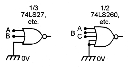
FIGURE 11. Basic ways of disabling unwanted TTL NOR gate inputs.
A NOR gate can be made to act as a simple inverter by either shorting all of its inputs together or by grounding all but one of its inputs; note, however, that the fan-in of a TTL NOR gate is directly proportional to the number of inputs used, so the first method is thus (theoretically) the best, since it offers the lowest fan-in value, as shown in Figure 12.
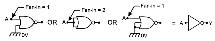
FIGURE 12. Ways of using a TTL NOR gate as a simple inverter.
NOR gates are fairly versatile devices. The effective number of inputs of a NOR gate can be increased by applying the extra inputs via a diode or IC OR gate, as shown in Figure 13.
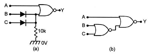
FIGURE 13. Ways of increasing the effective number of inputs of a NOR gate.
Figure 14 shows various ways of using two-input elements to make two-input or three-input OR gates or a three-input NOR gate.
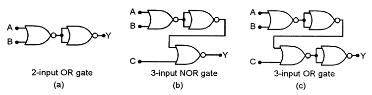
FIGURE 14. Ways of using two-input NOR gates to make various OR and NOR gates.
Note that a NOR gate can be converted into an AND gate by simply inverting all of its inputs. Figure 15 shows how three two-input NOR gates can be used to make a single AND gate.

FIGURE 15. NOR gates used to make a two-input AND gate.
Practical EX-OR and EX-NOR IC Circuits
The output of an EX-OR gate goes high only when its two inputs are at different logic levels. The most widely used EX-OR gate ICs are the 74LS86 TTL and the 74HC86 and 4070B CMOS Quad types (see Figures 16 and 17).
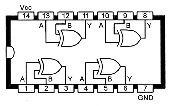
FIGURE 16. Functional diagram of the 74LS86 or 74HC86 Quad EX-OR gate IC.
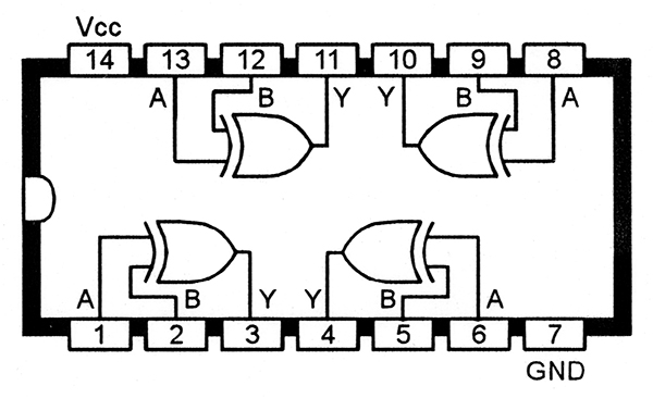
FIGURE 17. Functional diagram of the 4070B Quad EX-OR gate IC.
If one or more of a CMOS EX-ORIC’s gates are unwanted, it can be disabled by simply grounding both inputs. In the case of a TTL EX-OR IC, unwanted gates are best disabled by grounding one input terminal and tying the other high via a 1K resistor, as shown in Figure 18, as this results in minimum quiescent current consumption.
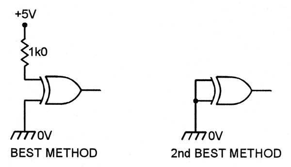
FIGURE 18. Two ways of disabling unwanted TTL EX-OR gates (see text).
Alternatively, if current drain is not important, both inputs can simply be tied to ground as shown.
EX-OR gates are quite versatile. An EX-OR gate can be made to act as a non-inverting buffer by simply grounding its unused input, as shown in Figure 19(a), or as an inverting buffer by tying the unused input high (via na 1K resistor in TTL types), as shown in Figure 19(b).
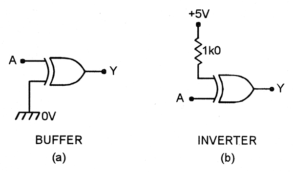
FIGURE 19. Ways of using TTL EX-OR gates as (a) buffers or (b) inverters.
Thus, two EX-OR gates can be used to make a single EX-NOR gate by connecting them as shown in Figure 20, where the right-hand gate is used to invert the output of the left-hand gate.
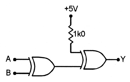
FIGURE 20. An EX-NOR gate made from two TTL EX-OR gates.
Note that Quad EX-NOR CMOS ICs are also available in dedicated IC forms as the 4077B and the 74HC266 (see Figures 21 and 22), but that the latter IC’s gates have open-drain outputs.
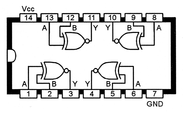
FIGURE 21. Functional diagram of the 4077B Quad EX-NOR gate IC.
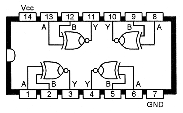
FIGURE 22. Functional diagram of the 74HC266 Quad EX-NOR gate IC with open-drain (o.d.) outputs.
Figures 23 and 24 show two other useful EX-OR gate applications. In Figure 23, four EX-OR gates are fed with a common control signal that enables a four-bit ‘ABCD’ input code to be presented in the form of eithera true (direct) or complemented (inverted) ABCD output, thus making the four-bit True/Complement outputs available via five (rather than eight) terminals.
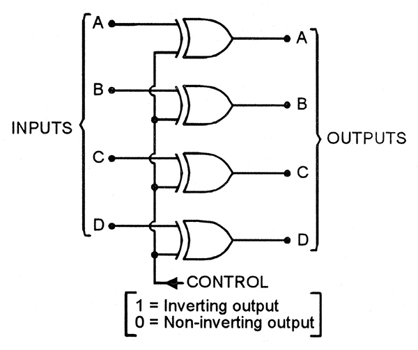
FIGURE 23. Four-bit True/Complement generator.
The circuit in Figure 24 simply compares the logic states of the two four-bit words and gives a logic 0 output if the two words are identical, and a logic 1 output if they differ.
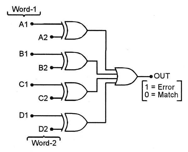
FIGURE 24. Four-bit logic state comparator.
One of the most important applications of the EX-OR gate is as a binary adder. Figure 25 lists the basic rules of binary addition.
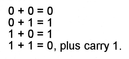
FIGURE 25. Basic rules of binary addition.
Figure 26 shows how an EX-OR and an AND gate can be used to make a practical half-adder circuit that can add two binary inputs together and generate SUM and CARRY outputs.
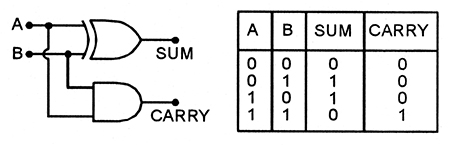
FIGURE 26. Binary half-adder circuit.
The circuit is called a half-adder because it can perform only a very primitive form of addition that does not enable it to accept a carry input from a previous addition stage. A full-adder is a far more useful circuit that can accept a carry input, perform two-bit binary addition, and generate a carry output; such circuits are fully cascadable, enabling groups of circuits to perform binary addition on digital numbers of any desired bit width.
Figure 27 shows one way of building a two-bit full-adder circuit, using three EX-OR gates, two AND gates, and an OR gate.
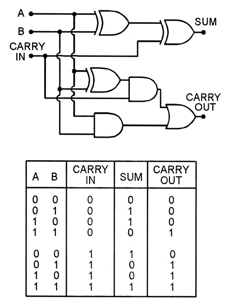
FIGURE 27. Full-adder circuit and truth table.
In practice, four-bit full-adders are readily available in the forms of the 74LS283 and 4008B ICs. NV