The first four parts of this series explained modern TTL and CMOS logic gate basics and gave practical descriptions of some of the most popular digital buffer, inverter, AND gate, NAND gate, OR gate, NOR gate, EX-OR gate, and EX-NOR gate digital ICs that are available. Now, in this final part of the series, we'll expand on this theme and describe a variety of popular digital mixed gate and special-purpose logic gate ICs such as programmable logic, majority logic, and digital transmission gate types that are available from either your local supplier or from specialist dealers.
Practical Mixed-Gate Digital ICs
The 74 and 4000B ranges of digital ICs include a number of mixed gate types that contain gates of more than one type, wired together for use in special applications. The best known of these are AND-OR-INVERT (AOI) gates, and examples of two of these are shown in Figures 1 and 2. It is unlikely that you will ever need to use an AOI gate, but you may find it useful to learn some of the jargon that is associated with them.
Looking first at the 7454 IC of Figure 1, note that it has input connections to four two-input AND gates, and this accounts for the four-wide two-input AND- part of the IC’s title; also note that the outputs of these four AND gates are wired to the input of a NOR gate and hence made externally available via pin 8.
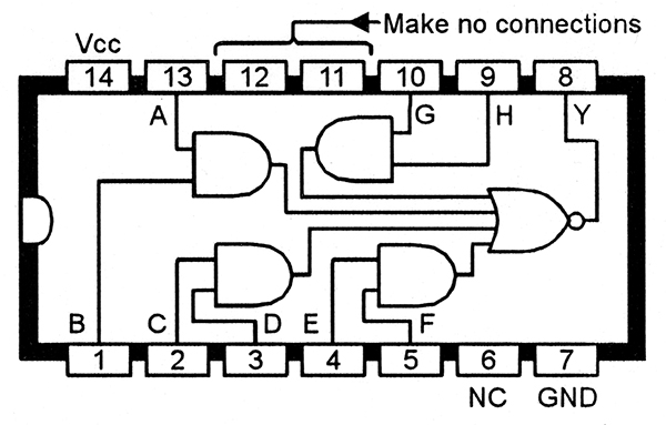
FIGURE 1. Functional diagram of the 7454 four-wide two-input AND-OR-INVERT (AOI) gate IC.
Now, a NOR gate is simply an OR gate with an inverted output, and this fact accounts for the OR-INVERT part of the IC’s title. Thus, an AND-OR-INVERT gate is simply an AND-NOR gate with a rather flowery title. The action of the 7454 IC is such that its output is normally high, and goes low only when both inputs to one or more AND gates are high.
Turning next to the 74LS55 IC of Figure 2, note that this has input connections to two four-input AND gates, and this accounts for the IC’s two-wide four-input AND-OR-INVERT title; the IC’s action is such that its output is normally high, and goes low only when all inputs to at least one AND gate are high.
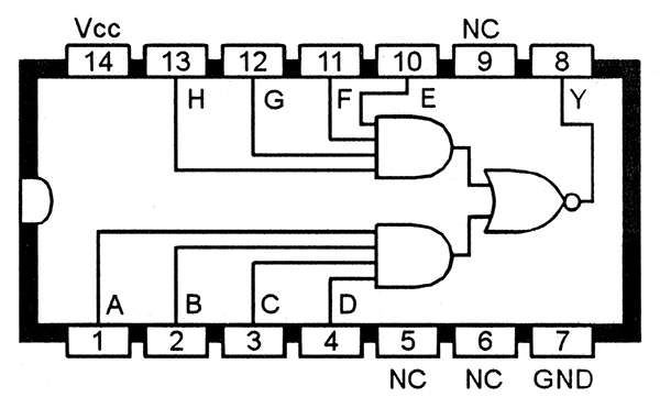
FIGURE 2. Functional diagram of the 74LS55 two-wide four-input AND-OR-INVERT gate IC.
Returning briefly to the 7454 IC, note that this is a standard TTL device, and its data sheet carries a very sinister warning that NO EXTERNAL CONNECTIONS must be made to pins 11 and 12. Also note that ‘LS’ versions of this device (the 74LS54) have two of its four AND gates configured as two-input types and two configured as three-input types, and is sometimes known as a four-wide, 2-3-3-2-input AND-OR-INVERT gate. It has pin connections that differ from those shown in Figure 1.
A Programmable Logic IC
Most logic ICs are dedicated devices that contain a number of fixed gates. One very useful exception is the CMOS IC known as the 4048B programmable eight-input multifunction gate (see Figure 3).
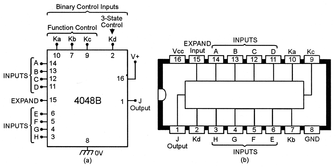
FIGURE 3. Functional diagram (a) and outline (b) of the 4048B multifunction expandable eight-input gate IC.
This modestly priced (but hard to find) 16-pin IC has two groups of four input terminals, plus an expansion input terminal, and is provided with four control (K) pins which let the user select the mode of logic operation, plus a J output terminal that enables 4048B ICs to be cascaded, so that two of them make a 16-input gate, or four make a 32-input gate, and so on.
Control input pin Kd (pin 2) enables the user to select either normal or high-impedance three-state output operation. The remaining three binary control inputs (Ka, Kb, and Kc) enable any one of eight different logic functions to be selected, as shown in the table of Figure 4, which also shows how to connect unwanted inputs in each mode of operation.
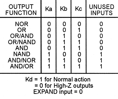
FIGURE 4. Function control diagram of the 4048B eight-input gate IC.
Thus, to make the 4048B act as a normal six-input OR gate, connect the two unwanted inputs to ground (logic 0), connect Ka and Kb to ground, and Kc and Kd to the positive supply rail. The EXPAND input (pin 15) is normally tied to ground.
Eight different logic functions are available from the 4048B, as shown in Figure 5.

FIGURE 5. The eight basic logic functions of the 4048B IC.
Operation in the AND, OR, NAND, and NOR modes is quite conventional, but operation in the remaining four modes (OR/AND, OR/NAND, AND/OR, and AND/NOR) is less self-evident. In the latter cases, the inputs are split into two groups of four, each of which provides the first part of the logic function, but the pair of groups provide the second part of the logic function. Thus, in the OR/AND mode, the IC gives a high output only if at least one input is present in the A-to-D group at the same time as at least one input is present in the E-to-H group, etc.
The EXPAND input terminal of the 4048B enables ICs to be cascaded; thus, two ICs can (for example) be made to act as a 16-input gate by feeding the output of one IC into the EXPAND terminal of the other. Note when using expanded logic that the input logic feeding the expand terminal is not necessarily the same as the overall logic that is required. Thus, an OR expand input is needed for expanded NOR or OR operation, a NAND expand for AND and NAND operation, a NOR expand for OR/AND or OR/NAND operation, and an AND expand for AND/OR and AND/NOR operations.
Majority Logic Circuits
One little known but useful type of logic system is majority logic, in which the logic device has an odd (3, 5, 7, etc.) number of inputs and gives an active output only when the majority of these inputs are high, irrespective of which inputs are high. This type of logic is useful in pseudo-intelligent alarms and robotic devices, etc., and may (for example) sound an alarm bell only if at least two of three detectors indicate a fault condition, or enable a robot to move only if there is more stimulus to move than there is to stand still, etc.
The best known CMOS majority logic IC is the 4530B dual five-input unit (Figure 6), each half of which contains a five-input majority logic element with its output feeding to one input of an EX-NOR gate that has its other input (W) externally available, enabling it to be wired as either an inverting or non-inverting stage.
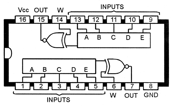
FIGURE 6. Functional diagram of the 4530B dual five-input majority logic gate IC.
Thus, when W is tied to logic 1, the EX-NOR stage gives non-inverting action and the element’s output goes high only when the majority of inputs are high. However, when W is tied to logic 0, the EX-NOR stage gives an inverting action and the element’s output goes high when the majority of inputs are low. Note that the effective number of inputs of a 4530B element can be reduced by wiring half of the unwanted inputs to logic 1 and the other half to logic 0, as in Figure 7(a). Alternatively, the effective number of inputs can be increased by cascading elements, with the output of one element feeding one input of the cascading element, as in Figure 7(b).
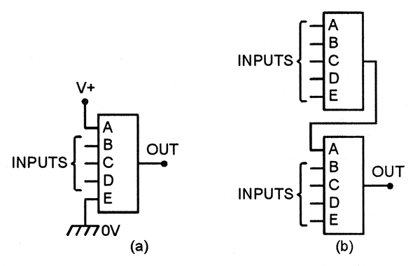
FIGURE 7. The number of effective inputs of a majority logic circuit can be (a) decreased or (b) increased easily.
In practice, the 4530B IC is often hard to find. In this case, a majority logic circuit can easily be built by wiring a 3140 CMOS op-amp in the basic configuration of Figure 8, which shows a five-input circuit.
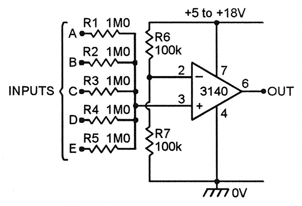
FIGURE 8. Simple five-input op-amp majority logic gate.
Here, the op-amp functions as a voltage comparator in which R6-R7 applies half of the supply voltage to pin 2 of the op-amp, and the five input resistors (which must each be connected to either ground or the positive supply rail) form a potential divider that applies a fraction of the supply voltage to pin 3.
This pin 3 voltage is lower than that of pin 2 if the majority of inputs are low, but greater than that of pin 2 if the majority of inputs are high. Under this latter condition, the op-amp output switches high, and this gives majority logic action.
Note that if 5% resistors are used, the Figure 8 circuit can be given any odd number of inputs up to a maximum of 11 by simply adding one more 1 meg resistor for each new input. The output of this circuit switches almost fully to zero volts when the output is low, but only rises to within a couple of volts of the positive rail when the output is high. In most applications this defect is of little importance; it does mean, however, that elements cannot be cascaded to increase the total number of inputs. This defect can be overcome by using the alternative configuration of Figure 9, in which the output is inverted and level-shifted by Q1, and the inputs to the op-amp are transposed.
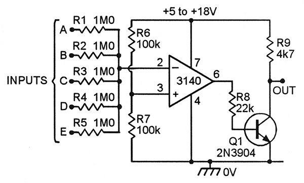
FIGURE 9. Compound five-input op-amp majority logic gate.
The output of this circuit switches to within 50 mV of either supply rail, enabling units to be cascaded without limit.
Assertion-Level Logic Notation
The reader is already familiar with the fact that an AND or OR gate has an active-high output (i.e., the output of an OR gate goes high when any input is high, etc.), and with the MIL/ANSI convention that the addition of a little circuit to an OR gate output (etc.) implies that the gate has an active low output, as shown in Figure 10.

FIGURE 10. Basic principles of assertion-level logic notation.
Technically, the presence or absence of this little circle is known as assertion-level logic notation, and can be legitimately applied both to the input or the output of a logic symbol.
Thus, the crude gated pulse generator symbol of Figure 11(a) implies that the pulse generator is gated on by a high input signal, but the modified symbol of (b) — in which a little circle is added to the generator’s input — implies that this generator is gated on by a low input signal, etc.
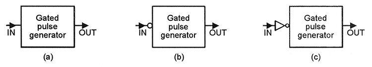
FIGURE 11. Pulse generators that can be gated-on by (a) logic 1 and (b,c) logic 0 inputs.
Note that in practice the (a) generator can be made to give the same action as that of (b) by simply inserting an inverter stage between the IN terminal and the input of the generator, as shown in (c), so that a low input forces the generator’s input high and gates it on. This system of assertion-level logic notation is, in fact, widely used in electronic logic symbology; some examples of its use are shown in Figure 12, which deals with mixed logic equivalents.
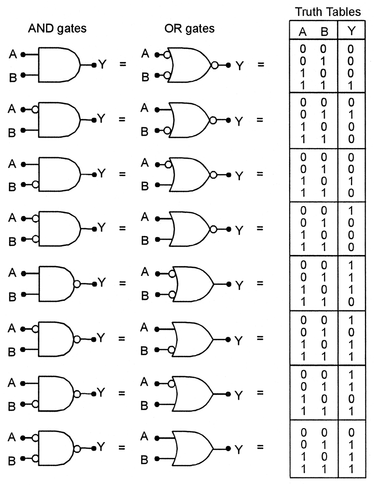
FIGURE 12. Mixed logic equivalents.
Mixed Logic Equivalents
When assertion-level logic notation is applied to a simple two-input AND or OR gate, it can be quickly seen that the gate has four possible input assertion-level sets, i.e., both inputs active-high, or both active-low, or one active-high and one active-low, or vice versa. Similarly, the gate’s output has two possible assertion-levels (active-high or active-low). Thus, a two-input AND or OR gate has a total of eight possible input/output assertion levels.
If Truth Tables are drawn up for all 16 possible AND and OR gate variations, it becomes apparent that each AND gate variation has a mixed-logic OR gate equivalent, and vice versa, as shown in Figure 12. Note in particular that a normal AND gate can be simulated by a NOR gate with both inputs inverted, and that a normal OR gate can be simulated by a NAND gate with both inputs inverted, etc.
Digital Transmission Gates
Most logic gate circuits presented in this five-part series show the gates used as simple logic state detectors. Two-input AND, NAND, OR, and NOR gates can, however, also be used as digital transmission gates which pass a digital input signal only when they are opened by an appropriate control signal or logic level.
Transmission gates are available in four basic types, and the logic symbols of these are shown, together with their logic gate equivalents, in Figure 13.
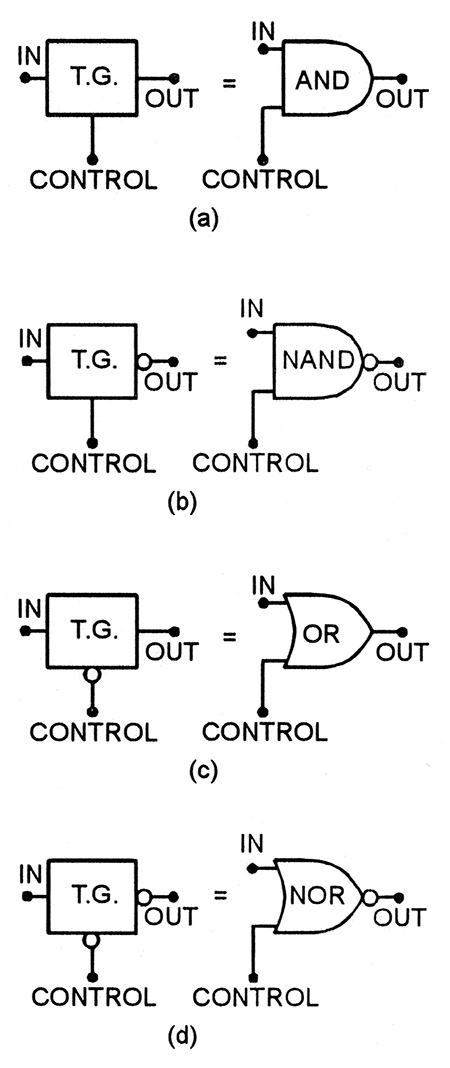
FIGURE 13. Four basic types of digital transmission gate, with their two-input logic equivalents.
The basic transmission gate (a) gives a non-inverted output, can be opened by a logic 1 control signal, and can be simulated by a two-input AND gate. This transmission gate can be made to give an inverted output, as in (b), by using a NAND gate instead of an AND gate. Another variation of the basic transmission gate is shown in Figure 13 (c); it gives a non-inverted output but is opened by a logic 0 control signal, and can be simulated by a two-input OR gate. This gate can be made to give an inverted output, as in (d), by using a NOR gate instead of an OR gate.
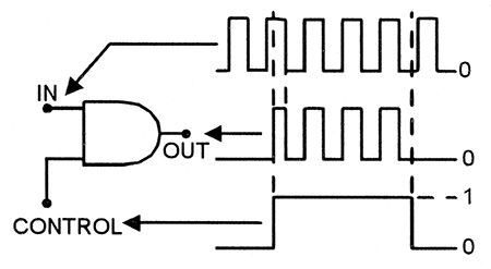
FIGURE 14. AND-type transmission gate is opened by logic 1 control and gives normally-low, non-inverted output.
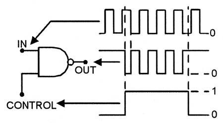
FIGURE 15. NAND-type transmission gate is opened by logic 1 control and gives normally-low, high-inverted output.
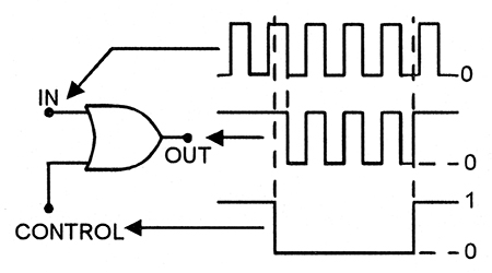
FIGURE 16. OR-type transmission gate is opened by logic 0 control and gives normally-high, non-inverted output.
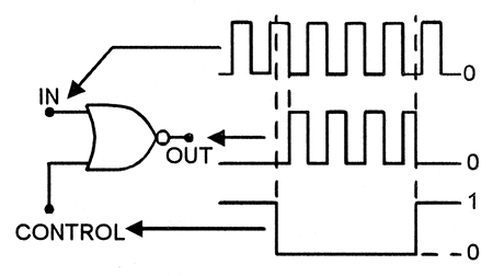
FIGURE 17. NOR-type transmission gate is opened by logic 0 control and gives normally-low, inverted output.
Finally, to conclude this final part, Figures 14 to 17 show the precise relationships between the input, output, and control signals of each of these four types of digital transmission gate. NV