Modern digital electronics are dominated by two major logic IC families: the low-speed ‘4000-series’ of CMOS ICs and the ‘74-series’ of fast TTL and CMOS ICs. The 74 family was originally based entirely on TTL technology, which first hit the electronics scene in a big way around 1972, when the 74-series suddenly arrived in the form of an entire range of versatile and cleverly conceived TTL digital logic ICs that were each designed to operate from a single-ended five-volt supply and to directly and easily interconnect with each other without hassle (each output could directly drive several inputs). This made it relatively easy for any moderately competent engineer to design and develop fairly complex digital logic systems. The series was an instant and brilliant international success, and almost immediately became the world’s leading IC logic system. Its ICs were produced in both commercial and military grades, and carried prefixes of 74 and 54, respectively; the commercial product range rapidly became known simply as the 74-series of ICs.
A major feature of the 74-series is that all devices within the range function as black boxes that operate at similar input and output threshold levels; the user does not need to understand their internal circuitry in order to use them, but simply needs to know their basic usage rules. Also, the input sensitivity or ‘fan-in’ of each device conforms to a fixed standard, and its output drive capability or ‘fan-out’ has a guaranteed minimum value that indicates the number of external 74-series inputs that it can safely directly drive, making it very easy to interconnect various devices. The output of a 74 gate with a fan-out of 10 can directly drive as many as 10 parallel-connected standard inputs on other 74-series ICs.
The type of TTL technology used in the initial (1972) 74-series ICs resulted in a range of devices that were moderately fast but consumed fairly heavy currents. Within a year or so, sub-families of the original TTL were introduced, offering a trade-off between speed and power, i.e., twice the speed but at twice the current consumption (in the H or high speed sub-family), or one-tenth of the current consumption but only one-third of the normal speed (in the L or low power sub-family), etc.
This trend of seeking a good or ever-better trade-off between speed and power consumption has continued until present day, and so far, a total of eight commercially successful sub-families of TTL (and five sub-families of CMOS) have appeared in the 74-series of digital ICs. Many of these sub-families have subsequently become obsolete or obsolescent, but the practical design/maintainance engineer or technician still needs a basic knowledge of all of them, since they are often found in old equipment that needs repairing or upgrading.
Note that each sub-family of the 74-series of ICs is almost directly compatible with all other sub-families in the series. Thus, if you open up an old piece of equipment and find (for example) that an old 74L90 decade counter IC needs replacing but is no longer available, you will probably find that a modern 74LS90 decade counter IC can be used as a direct plug-in replacement, or that any other 74XX90 ICs can be used as a replacement either directly or with slight circuit modification (depending on the basic characteristics of the two sub-families). In either case, the first thing that you will need to do is identify the device of interest from its printed code number. Figure 1 explains the basic scheme that is used in formating the 74-series code numbers.
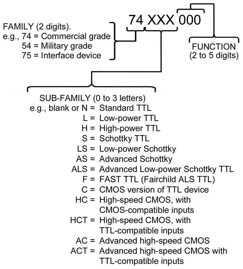
FIGURE 1. Basic coding system used on the 74-series ICs.
All ICs in the 74 family are identified by an alpha-numeric code which — in its simplest form — consists of three sub-codes strung together as shown in Figure 1. The first (left hand) sub-code consists of two digits that read either 74, 54, or 75. The 74 identifies the IC as a commercial-grade member of the family. These devices are usually encapsulated in a plastic 14-pin, 16-pin, or 24-pin dual-in-line package (DIP), can be used with supplies within the limit +4.75 V to +5.25 V, and can be operated over the temperature range 0° C to +70° C. The 54 identifies the IC as a high-quality military-grade member of the family. These devices are encapsulated in exotic packages, can use supplies within the limit +4.5 V to +5.5 V, and can operate over the temperature range -55° C to +125° C. The 75 identifies the IC as a commercial-grade interface device that is designed to support the 74 range of devices.
The second (central) sub-code consists of up to three letters, and identifies the precise technology or sub-family used in the construction of the device, as shown in the diagram. Note that standard TTL devices carry either no central code at all, or an N. Each of the other seven major TTL sub-family devices carry a central identifying code, and the five major CMOS 74 sub-families carry a central code that includes the letter C.
The last (right hand) sub-code usually consists of two to five digits (but occasionally includes a letter A or a star), and identifies the precise function of the IC (e.g., quad two-input NAND gate, decade counter, four-bit shift register, etc.). The precise relationship between this sub-code and the device function can be ascertained from the manufacturer’s lists.
Thus, a 74 type of IC may carry a code that, in its simplest form, reads something like 7400, 74N00, or 7414, etc., if it is a standard TTL device, or 74L14, 74LS38, or 74HC03, etc., if it is some other sub-member of the 74 family. Note that in practice 74-series ICs often carry an elaborated form of the basic code that includes a two-letter pre-fix that identifies the manufacturer, plus a lettered manufacturer’s suffix that indicates the packaging style, etc., as shown in Figure 2.
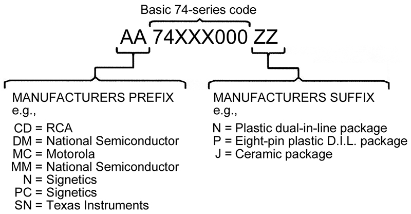
FIGURE 2. The basic 74-series code is often elaborated with a manufacturer’s prefix and/or suffix.
Hence, a device marked SN74LS90N is a normal 74LS90 IC, manufactured by Texas Instruments and housed in a plastic DIP.
TTL Sub-Families
Eight major sub-families of TTL have been used in the 74-series throughout its lifetime, as follows:
Standard TTL — Standard TTL is similar to the basic type already described, except that each of its inputs are provided with a protection diode that helps suppress transients and speeds up its switching action. Figure 3 shows the actual circuit of a 7400 two-input NAND gate. Its power consumption is 10 mW, and its propagation delay is 9 nS when driving a 15pF/400Ω load.
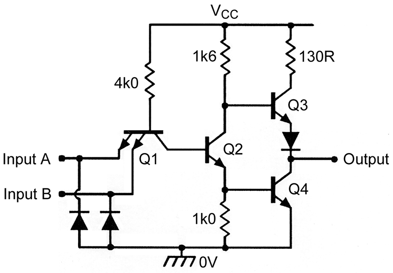
FIGURE 3. Circuit of a Standard TTL 7400 two-input NAND gate.
Low-Power (L) TTL (now obsolete) — Low-power TTL is a modified version of the standard type, with its resistance values greatly increased to give a dramatic reduction in power consumption at the expense of reduced speed. Figure 4 shows the circuit of a 74L00 two-input NAND gate. Its power consumption is 1 mW, and its propagation delay is typically 33 nS.
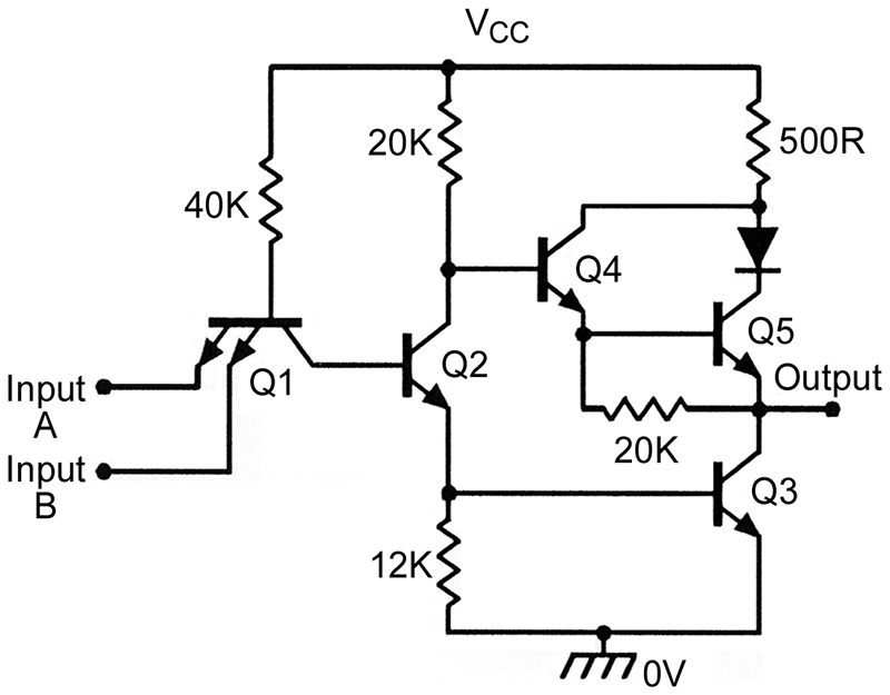
FIGURE 4. Circuit of a low-power (L) TTL 74L00 two-input NAND gate.
High-Speed (H) TTL (now obsolete) — High-speed TTL is a modified version of the standard type, with its resistance values reduced to give an increase in speed at the expense of increased power consumption. Figure 5 shows the circuit of a 74H00 two-input NAND gate. Its power consumption is 22 mW, and its propagation delay is typically 6 nS.
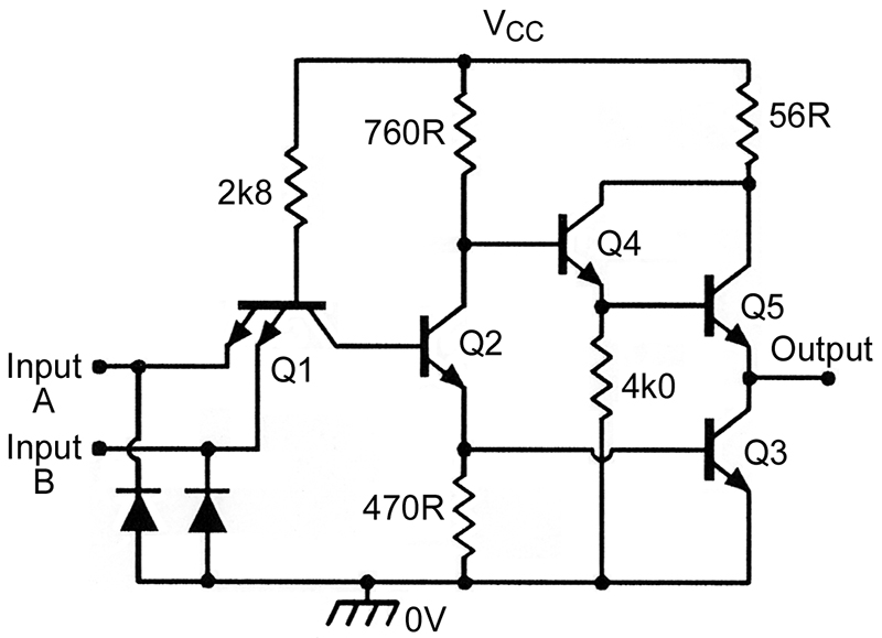
FIGURE 5. Circuit of a high-speed (H) TTL 74H00 two-input NAND gate.
Schottky (S) TTL (now obsolete) — A transistor switch can be designed to give either a saturated or an unsaturated switching action. Saturated switching — in which the transistor’s collector voltage falls far below that of the base under the on condition — is very easy to implement, but produces propagation delays that are about 2.5 times longer than those available from unsaturated circuits.
Standard TTL operates its transistors in a heavily-saturated switching mode in which the collector falls some 400 mV below the base under the on condition, and is thus intrinsically slow. Schottky TTL, on the other hand, operates its transistors in a lightly-saturated switching mode in which the collector only falls some 180 mV below the base voltage under the on condition, and is almost as fast as an unsaturated circuit (such as an ECL design).
Basically, this action is achieved by connecting a Schottky diode (which is fast-acting and has a typical forward volt drop of only 180 mV) between the transistor’s collector and base as shown in Figure 6(a), in which Rs represents the input pulse’s source impedance. Thus, if the collector goes more than 180 mV negative to the base, the Schottky diode becomes forward-biased and starts to shunt base current directly into the transistor’s collector, thus automatically preventing deeper saturation. In reality, the Schottky diode can easily be incorporated in the transistor’s structure, and a ‘Schottky-clamped transistor’ of this type uses the symbol shown in (b).
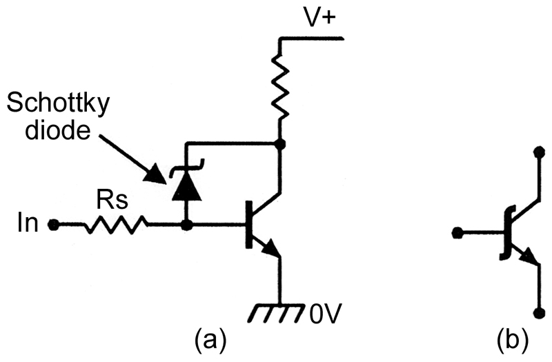
FIGURE 6. (a) A Schottky diode used to limit the saturation depth of an NPN transistor; (b) Symbol of an NPN ‘Schottky’ transistor, with a built-in clamping diode between its collector and base.
In a practical Schottky TTL IC, Schottky-clamped transistors are widely used, and most resistance values are reduced, thus giving a good increase in speed at the expense of power consumption. The totem-pole output stage uses a Darlington transistor pair to give active pull-up, plus a modified active pull-down network that gives an improved waveform-squaring action. Figure 7 shows the circuit of a 74S00 two-input NAND gate. Its power consumption is 20 mW and its propagation delay is 3 nS when driving a 15pF/280Ω load.
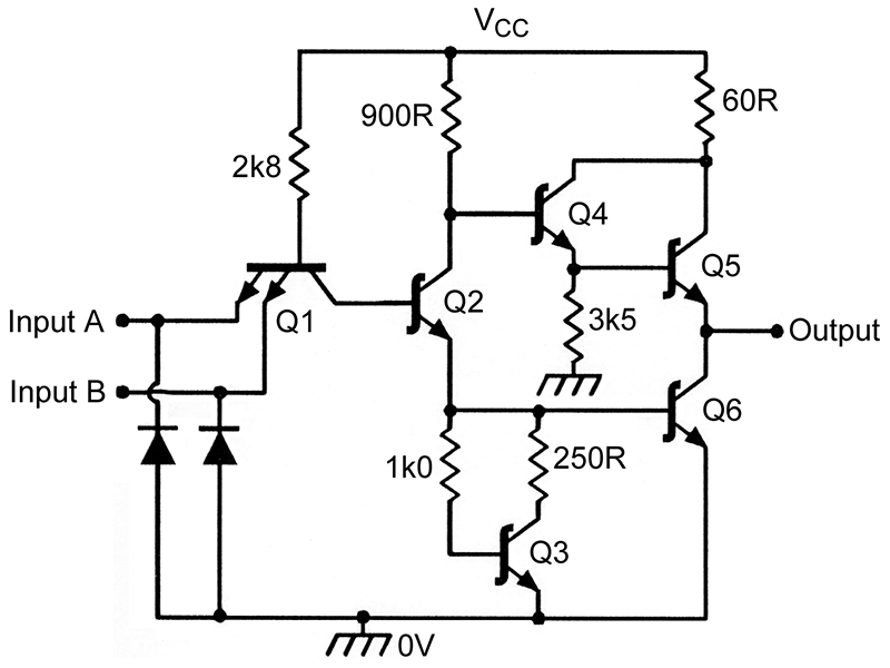
FIGURE 7. Circuit of a Schottky (S) TTL 74S00 two-input NAND gate.
Low-Power Schottky (LS) TTL — Low-power Schottky uses a modified form of Schottky technology, using improved manufacturing techniques, combined with a diode-transistor (rather than multi-emitter) form of input network that has a high impedance and gives fast switching. Figure 8 shows the circuit of a 74LS00 two-input NAND gate. Its power consumption is 2 mW and its propagation delay is 8 nS when driving a 12pF/2K load.
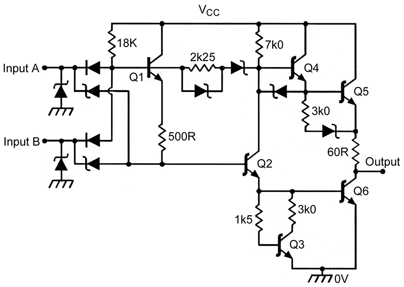
FIGURE 8. Circuit of a low-power Schottky (LS) TTL 74LS00 two-input NAND gate.
Advanced Low-Power Schottky (ALS) TTL — This sub-family is similar to LS but uses an advanced fabrication process which, combined with minor design modifications, yields active devices that are faster and have higher gains than LS types. Figure 9 shows the circuit of a 74ALS00 two-input NAND gate. Its power consumption is 1 mW and its propagation delay is 4 nS when driving a 50pF/2K load.
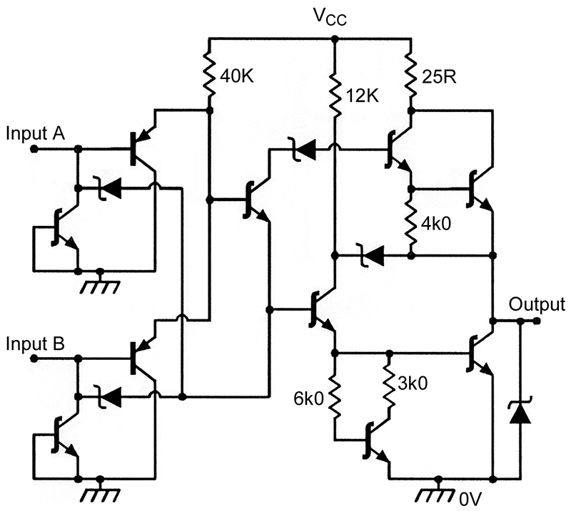
FIGURE 9. Circuit of an advanced low-power Schottky (ALS) 74ALS00 two-input NAND gate.
Advanced Schottky (AS) TTL — This sub-family is similar to ALS, but its design is optimized to give very high speed at the expense of power consumption. Figure 10 shows the circuit of a 74AS00 two-input NAND gate. Its power consumption is 22 mW and its propagation delay is a mere 2 nS when driving a 50pF/2K load.
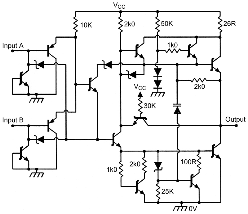
FIGURE 10. Circuit of an advanced Schottky (AS) TTL 74AS00 two-input NAND gate.
FAST (F) TTL — FAST (Fairchild Advanced Schottky TTL) is Fairchild’s version of ‘AS’ TTL. It is manufactured under license by several companies (including Philips and National Semiconductor). Its performance is similar (in terms of speed and power consumption) to that of the AS sub-family.
CMOS 74-Series Sub-Families
When the 74-series of ICs were first released in 1972, all devices in the range were based on bipolar TTL technology, which inherently consumes a fairly large amount of power, irrespective of its operating speed. In about 1975, the rival CMOS digital ICs technology arrived on the scene, and although it was not as fast as TTL, it offered the outstanding advantage of having a power consumption that was directly proportional to operating speed, being virtually zero under quiescent conditions and rising to the same value as TTL at about 10 MHz. In the late 1970s, CMOS was introduced as a sub-family within the 74-series range of devices, carrying the central code C. The graph in Figure 11 compares the frequency/current-consumption curves of a single gate from the standard TTL and the CMOS C versions of the 7400 quad two-input NAND gate IC.
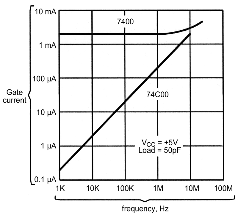
FIGURE 11. Frequency-current graphs of 7400 (TTL) and 74C00 (CMOS) two-input NAND gates (with a squarewave input).
In its early form, the 74-series C sub-family was slow and had a very weak output-drive capability (its fan-out drive was equal to two L type inputs). In subsequent years, however, considerable improvements took place in both the design and production of CMOS-type devices. The salient details of this subject will be covered in greater detail in Part 4, but in the meantime, it is sufficient to know that a total of five CMOS sub-families have been introduced in the 74-series, as follows:
Standard (C) CMOS (now obsolete) — This sub-family was virtually normal CMOS in a 74-series format. Typically, a single 74C00 two-input NAND gate consumed about 15 mW at 10 MHz, and had a propagation delay of 60 nS.
High-Speed (HC) CMOS — In the early 1980s, advances in CMOS fabrication techniques yielded speed performances similar to LS TTL, but with CMOS levels of power consumption. HC 74-series devices using this technology have CMOS-compatible inputs. Typically, a single 74HC00 two-input NAND gate consumes less than 1µA of quiescent current, and has a propagation delay of 8 nS.
High-Speed (HCT) CMOS — These are HC-type devices, but have TTL compatible inputs. Typically, a 74HCT00 two-input NAND gate consumes less than 1µA of quiescent current and has a propagation delay of 18 nS.
Advanced High-Speed (AC) CMOS — In the late 1980s, advances in CMOS design and further advances in CMOS fabrication techniques yielded speed performance similar to those of ALS. AC 74-series devices using this technology have CMOS-compatible inputs. Typically, a 74AC00 two-input NAND gate has a propagation delay of 5 nS.
Advanced High-Speed (ACT) CMOS — These are AC-type devices, but have TTL-compatible inputs. Typically, a 74ACT00 two-input NAND gate has a propagation delay of 7 nS.
Which Logic Family is Best?
Two major general-purpose logic families are currently available: the 4000-series low-speed CMOS family and the high-speed 74-series TTL/CMOS family (a third family, using ECL technology, is very specialized and intended for use in very high-speed applications). The 4000-series (which will be described in Part 4) is of particular value in circuits operating below frequencies of a few MHz in which a minimal figure of quiescent current consumption is desired. Other major advantages of the series are that its ICs can operate from any supply in the 3 to 15 V range, have excellent noise immunity, and have ultra-high input impedances.
The 74-series is of special value in circuits operating at frequencies up to several tens of MHz, in which low quiescent current consumption is not too important and in which the ICs can be powered from a well-regulated DC supply (typically of +5 V). If you decide to use a 74-series IC, you are faced with the problem of deciding “which sub-family is best for my application?”
Which 74-Series Sub-Family is Best?
When designing a new logic circuit, ICs should always be selected on a basis of commercial (rather than purely technical) superiority. It would, for example, be foolish to use a really fast ALS gate in an application in which a slower LS or HC device would be perfectly adequate and was readily available at a fraction of the cost of the ALS device. With this point in mind, note that the five 74-series IC sub-families most widely available at the time of writing are Standard and LS TTL, and HC, HCT and AC CMOS. Of these, Standard TTL is technically and commercially inferior to LS and is not recommended for use in new designs. The AC CMOS cost approximately 2.5 times as much as LS TTL or HC/HCT CMOS and should thus only be used in special applications. HCT is only meant to be used as a replacement for TTL devices in existing designs and should not really be used in new designs. That leaves just LS TTL and HC CMOS.
Of these two 74-series sub-families, LS is slightly faster than HC and is available in a far greater range of functional device types, but generally consumes more supply current/power than HC at frequencies below about 5 MHz. (Figure 12 compares the performances of 74LS00 and 74HC00 gates.)
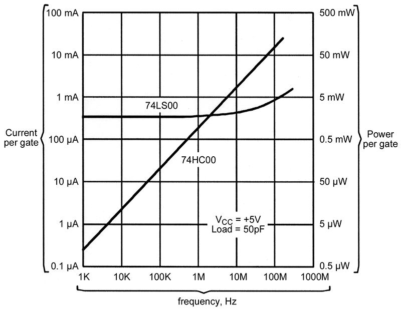
FIGURE 12. Frequency versus current/power graphs of 74LS00 and 74HC00 two-input NAND gates (with a square wave input).
Thus, for most new design applications, the LS TTL and HC CMOS sub-families deserve a joint ‘best’ award, with a slight edge perhaps going to LS.
TTL Logic Levels and Noise Immunity
All digital ICs handle input and output signals that switch between the high (logic-1) or low (logic-0) states. In TTL, each of these logic levels must fall within a defined range of voltage limits. Figure 13 shows the typical input-to-output voltage curve of a Standard TTL inverter that operates from a +5 V supply and has a lightly loaded output.
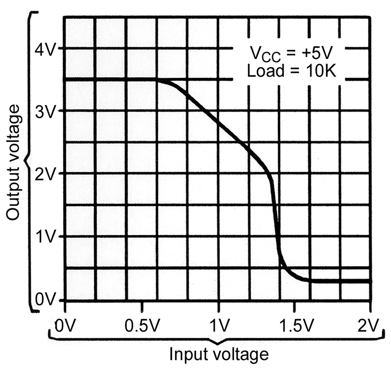
FIGURE 13. Standard-TTL input-to-output voltage graph.
Note that the output is high, at +3.5 V, until the input rises to 0.7 V, and then falls fairly linearly as the input is further increased, and eventually stabilizes at a low value of about 0.25 V when the input rises above 1.5 V.
In practice, all Standard and LS TTL ICs are — when using a +5 V supply — guaranteed to recognize any input voltage of up to 0.8 V as being a logic-0 input, and of 2.0 V or above as being a logic-1 input. Note that the area between these two levels is known as the IC’s indeterminate zone or region, and operation within this zone should be avoided.
In TTL circuitry, different logic levels are used to define input and output signals, since TTL output voltage levels vary considerably with loading conditions. Figure 14 shows how — when an input of 0.4 V is applied to the above TTL inverter — the logic-1 output voltage falls from +3.5 V at near-zero load current, to a mere 2.0 V at a load current of 13 mA, and so on.
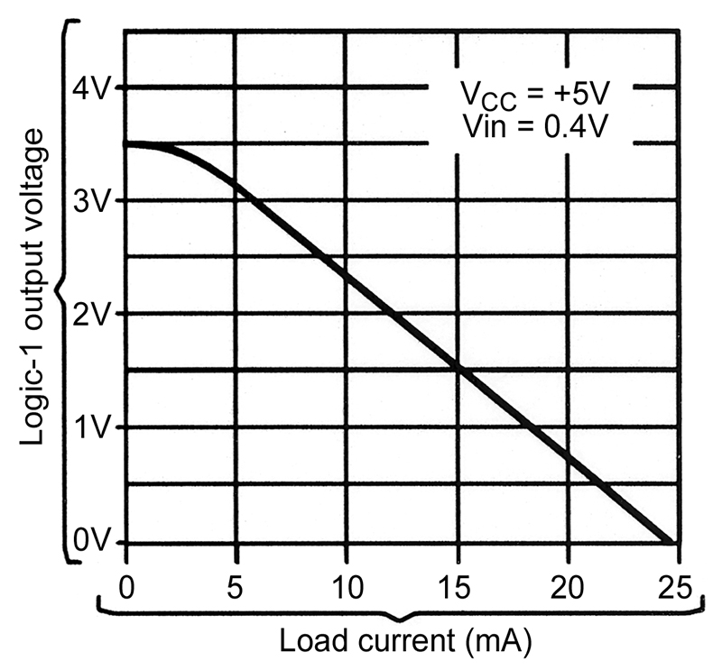
FIGURE 14. Standard-TTL logic-1 output voltage-current graph.
In practice, all Standard TTL ICs are guaranteed (when using a +5 V supply) to recognize any output voltage of up to 0.4 V as being a logic-0 output, and of 2.4 V or above as being a logic-1 output. On LS TTL ICs, these levels are 0.5 V for logic-0, and 2.7 V for logic-1.
When one TTL output is connected directly to a following TTL input, any excessive noise on the output signal may cause incorrect operation of the following input stage. Thus, taking a worst-case situation, a logic-1 Standard TTL output may be as low as 2.4 V, and any superimposed negative-going noise pulse greater than 0.4 V will drive the following input below the 2.0 V ‘logic-0’ defined threshold and may cause it to erroneously recognize its input as being a logic-0 (rather than logic-1) signal.
The maximum worst-case magnitude of noise that a digital IC can ignore under these conditions is known as its noise immunity or noise margin value, and equals the difference between the logic-0 or logic-1 output/input threshold values. With Standard TTL, noise margins for both logic-1 (NM-H) and logic-0 (NM-L) have defined worst-case values of 400 mV. With LS TTL, the noise margins are 700 mV for logic-1, and 300 mV for logic-0. With CMOS, both margins have values of VDD/3. Figure 15 illustrates the values of these three sets of threshold and margin values.
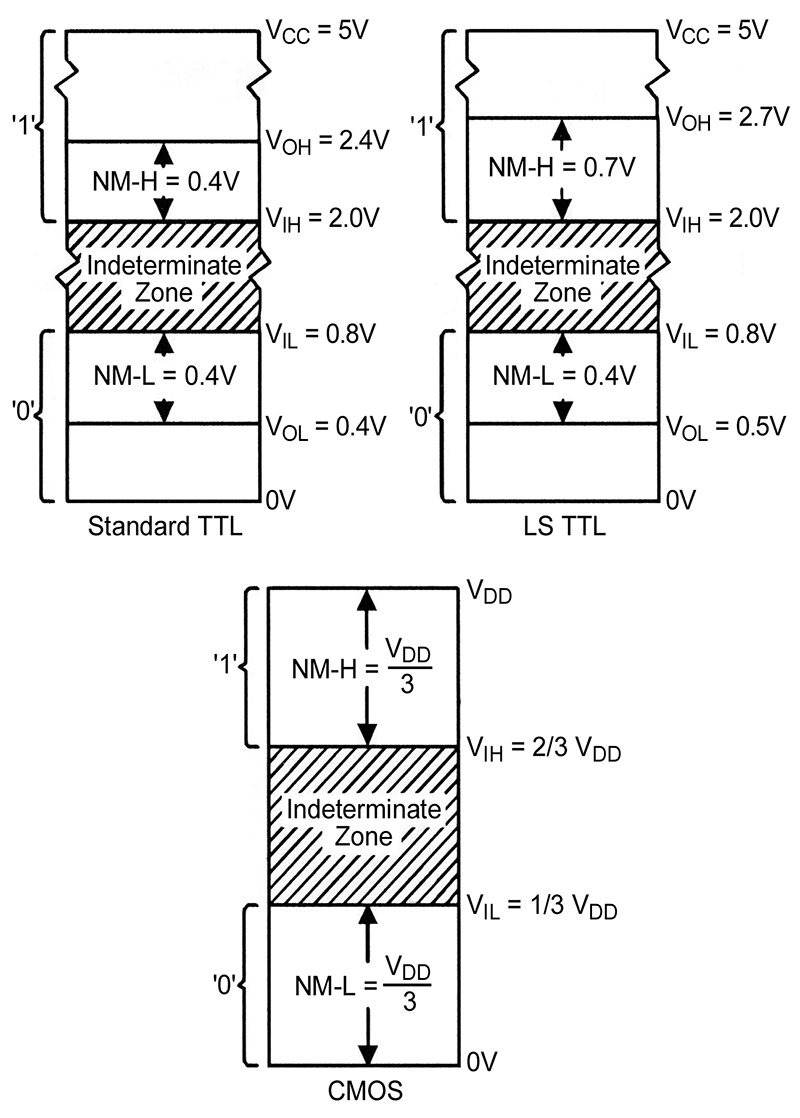
FIGURE 15. Logic level and noise margin values of Standard TTL, LS TTL, and CMOS.
Figure 16 expands the above information and shows actual defined threshold voltage and noise margin values, together with typical propagation and power dissipation values for single 00-type two-input NAND gates, for the seven major sub-families of TTL (FAST TTL is regarded here as simply a minor variation of AS TTL).

FIGURE 16. Typical propagation delay and power dissipation figures for single 00-type NAND gates within the TTL sub-family ranges, together with sub-family voltage threshold and noise-margin values.
Fan-In and Fan-Out
In TTL circuitry, an element’s input drive requirements are known as its fan-in values, and its output driving capability limits are known as its fan-out values. Figure 17 illustrates the meanings and worst-case values of these items when applied to a Standard TTL element.
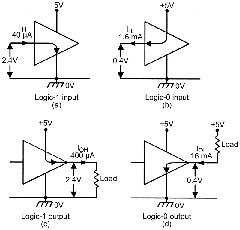
FIGURE 17. Basic input and output parameters of a Standard TTL logic element.
Thus, (a) shows that when the TTL element is driven from a Standard TTL output stage, it draws a worst-case input current (IIH) of 40µA when fed with a 2.4 V logic-1 input, but — as shown in (b) — feeds 1.6 mA (IIL) into the driver when it provides a 0.4 V logic-0 input. Diagram (c) shows that the TTL element’s output can, when in the logic-1 state, provide up to 400µA (IOH) before its output voltage falls below 2.4 V; it is thus capable of feeding up to 10 Standard inputs, and is said to have a logic-1 fan-out (= IOH/IIH) of 10.
Similarly, (d) shows that the output stage can — when in the logic-0 state — absorb up to 16 mA before its output voltage falls below 0.4 V; it is thus capable of driving up to 10 Standard inputs, and is said to have a logic-0 fan-out (= IOL/IIL) of 10. Thus, the element has a worst-case fan-out of 10, and it can be used to directly drive as many as 10 Standard inputs.
Figure 18 presents the above data in tabular form, together with similar data for all other major TTL sub-families.
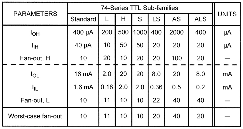
FIGURE 18. Fan-in and fan-out values of the major TTL sub-families.
When working within any one sub-family, note that the most important figure here is the ‘worst case fan-out (F-O)’ value. Thus, if you are (for example) designing a system based entirely on LS ICs, you can confidently connect an ordinary output directly to as many as 20 normal inputs, without risk of a malfunction due to overloading (if you need to drive more than 20 inputs, you can do so via one or more high-fan-out buffers, etc.). Note that, within any given sub-family, all ordinary inputs are said (in TTL jargon) to have a fan-in of unity (1), but that in practice some MSI or LSI ICs (such as counters and registers, etc.) may have special inputs (such as Reset or Preset, etc.) with fan-in values of two or greater.
Sometimes, an engineer may have to mix TTL sub-families, usually so that an obsolete IC can be replaced by a readily-available modern plug-in close-equivalent. In such a case, it is necessary to relate the fan-out data of one sub-family to that of another, to check that the mix can be made without causing an input or output overload. One easy way of doing this is to simply transpose the data of Figure 18 into ‘Standard TTL’ fan-in units, as shown in Figure 19, to gain an approximate idea of the relative fan values of various sub-families. Thus, it can be seen at a glance that LS TTL has only half of the fan-in requirement of Standard TTL, but also has only half of its fan-out capability, etc.
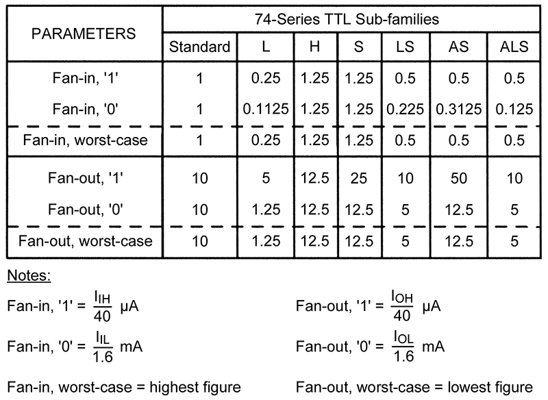
FIGURE 19. TTL fan-in and fan-out in terms of Standard TTL units.
An even more useful way of applying the basic data of Figure 18 is to convert it into an easily-used form that relates the fan-in and fan-out data of each TTL sub-family to all other TTL sub-families, as shown in Figure 20.
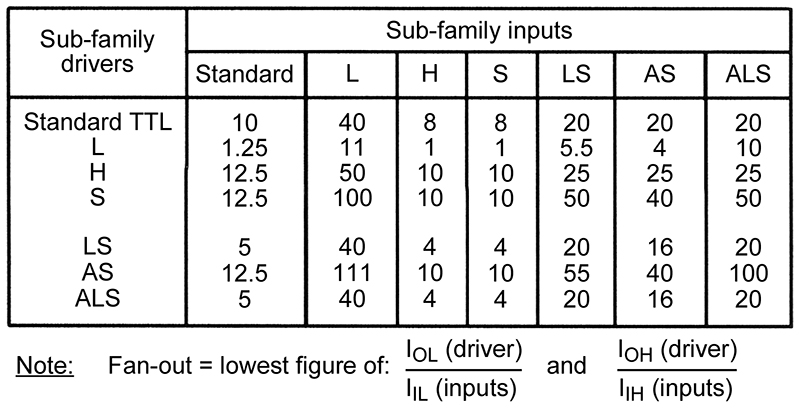
FIGURE 20. Maximum number of TTL inputs that may be driven from any TTL sub-family output.
Here, by reading across the left-hand columns, it can (for example) be seen that a normal LS output can drive up to five Standard TTL inputs, and that a Standard TTL output can safely drive up to 20 LS inputs.
Thus, if an engineer is faced with a problem such as that illustrated in Figure 21 — in which a fault on an old Standard TTL circuit is traced to a defective 74XXX-type IC (IC2) which is used to directly drive four other Standard TTL inputs — it can be quickly seen that a 74LSXXX plug-in equivalent IC can be safely used to directly replace the IC2 Standard TTL device without incurring overload problems.
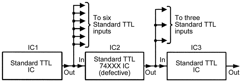
FIGURE 21. IC2 is defective; it is a Standard TTL device. Can it be replaced directly by a 74LSXXX IC? Figure 20 shows that the answer is yes.
TTL Basic Usage Rules
It is usually a fairly easy matter to design logic circuitry using TTL ICs, providing that a set of TTL basic usage rules are observed. Assuming that the matter of fan-in and fan-out has already been taken care of, there are four basic usage themes outstanding, and these will be described in our next installment, under the general headings of Power Supplies, Input Signals, Unused Inputs, and Interfacing. NV