It is usually a fairly simple matter to design logic circuitry using “74-series” TTL ICs, provided that a set of TTL basic usage rules are observed. Assuming that the matter of fan-in and fan-out has already been taken care of (as described in Part 2 of this mini-series), four other basic usage themes remain, and these are described under the headings Power Supplies, Input Signals, Unused Inputs, and Interfacing.
Power Supplies
The 74-series TTL ICs are designed to be used over a very limited supply voltage range (4.75-5.25 V), and — because they generate very fast pulse edges and have relatively low noise-margin values — must be used with supplies with very low output impedance values (typically less than 0.1 Ω). Consequently, practical TTL circuits should always be powered from a low-impedance, well-regulated supply such as one of those shown in Figures 1 to 3, and must be used with a PCB (printed circuit board) that is very carefully designed to give excellent high-frequency supply decoupling to each TTL IC.
In general, the TTL circuit’s PCB’s +5 V and 0 V supply rail tracks must be as wide as possible (ideally, the 0 V track should take the form of a ground plane). Connections and interconnections should be as short and direct as possible. The PCB’s supply rails should be liberally sprinkled with 4.7 µF tantalum electrolytic capacitors (at least one for every 10 ICs) to enhance low-frequency decoupling, and with 10 nF disk ceramics (at least one for every four ICs, fitted as close as possible between an IC’s supply pins) to enhance high-frequency decoupling.
Three power-supply circuits are shown in Figures 1 to 3. These are typical TTL PSU designs, and all work basically the same way. In each case, the AC input voltage is stepped down to a value in the 9-12 V range via transformer T1 (which has a VA power rating at least double that of the final power supply’s DC output). The resulting T1 output is full-wave rectified via bridge rectifier BR1 and converted into a reasonably smooth DC voltage via electrolytic capacitor C1.
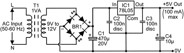
FIGURE 1. A 5 V regulated DC supply (100 mA maximum output).
The DC output of C1 is then converted into a smooth and stable 5 VDC via a 7805-type 5 V voltage regulator IC1 (which requires an input voltage that is at least 3 V greater than the specified output voltage). In Figure 1, IC1 has a 100 mA current rating, as implied by the L in the middle of the IC’s type code. In Figures 2 and 3, IC1 has a 1-A current rating and must be fitted to a suitable heatsink.
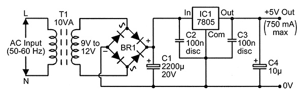
FIGURE 2. A 5 V regulated DC supply (750 mA maximum output).
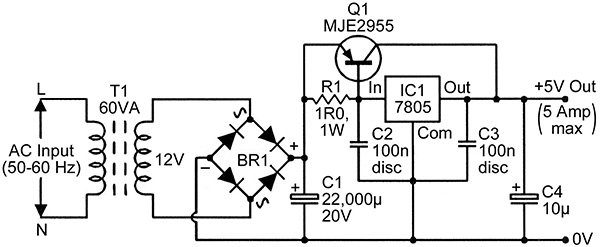
FIGURE 3. A 5 V regulated DC supply (5 A maximum output).
Note that — in Figure 3’s circuit — the available output current is also shunt-boosted to a total of about 5 A via Q1 and current-sensing resistor R1. At low currents, insufficient voltage is developed across R1 to turn on Q1, so all the load current is provided by the IC. At load currents of 600 mA or greater, however, sufficient voltage (600 mV) is developed across R1 to turn on Q1. Q1 thus provides most of the load currents in excess of 600 mA.
Note in the above three circuits that the ripple voltage generated across smoothing capacitor C1 is directly proportional to the regulator’s output load current. As a rough rule of thumb, in a full-wave rectified power supply, operating from a 50-60 Hz power line via a step-down transformer, an output load current of 100 mA will cause a ripple waveform of about 700 mV peak-to-peak to be developed on a 1,000 µF filter capacitor.
The amount of ripple is directly proportional to the load current and inversely proportional to C1’s capacitance value. Thus, the circuit in Figure 1 — which has a C1 value of 470 µF — generates a C1 peak-to-peak ripple voltage of about 1.4 V at its rated output current of 100 mA. The circuit in Figure 2 (C1 = 2,200 µF) generates a C1 peak-to-peak voltage of about 2.4 V at its rated output current of 750 mA, and the circuit in Figure 3 (C1 = 22,000 µF) generates a C1 peak-to-peak voltage of about 1.6 V at its rated output of 5 A. At the output of each circuit, these ripple values are reduced by about 80 dB by the action of IC1.
Input Signals
When using TTL, all IC input signals must — unless the IC is fitted with a Schmitt-type input — have very sharp rising and falling edges (typical rise and fall times should be less than 40 nS on LS TTL, for example). If rise or fall times are too long, they may allow the input terminal to hover in the TTL element’s linear indeterminate zone (see part 2 of this series) long enough for the element to burst into wild oscillations and generate spasmodic output signals that may disrupt associated circuitry (such as counters and registers).
If necessary, slow input signals can be converted into fast ones by feeding them to the IC’s input terminal via an inverting or non-inverting Schmitt element, as shown in Figure 4.
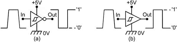
FIGURE 4. Slow input signals can be converted into fast ones via (a) an inverting or (b) non-inverting Schmitt element.
In practice, these simple circuits can be cheaply implemented by using a 74LS14 (or similar) IC that houses six Schmitt inverter elements. Two of these elements can be cascaded to make one non-inverting Schmitt element. All unused elements should be disabled by connecting their inputs directly to the 0 V rail (see the next paragraph for a deeper description).
Unused Input
Unused TTL input terminals should never be allowed to simply float, since this makes them susceptible to noise pick-up, etc. Instead, they should be tied to definite logic levels, by connecting them to VCC via a 1K resistor, by shorting them directly to the ground rail, or by connecting them to a TTL input or output terminal that is already in use.
Figure 5 shows examples of the four options. The simplest option is to tie the unused input to VCC via a 1K resistor, as shown in Figure 5(a). This resistor has to supply only a few microamperes of current (IIH) to each input, and can thus easily drive up to 10 unwanted inputs. Alternatively, the input can be tied directly to ground, as in Figure 5(b), but in that case, an input current of several hundred microamperes (IIL) may flow to the ground rail via the input.
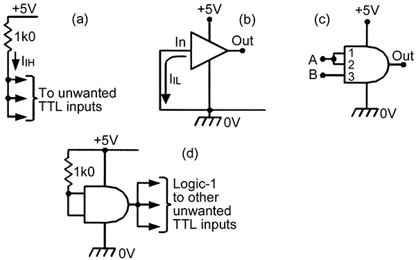
FIGURE 5. Alternative ways of connecting unwanted TTL inputs (see text).
If the unwanted input is on a multi-input gate, it can be disabled by shorting it to one of the gate’s used inputs, as in Figure 5(c), where a three-input AND gate is shown used as a two-input type. If the IC is a multiple-gate type, and an entire gate is unwanted, that gate should be disabled by tying its inputs high if it is a non-inverting (AND or OR) type, or shorting them to ground if it is an inverting (NAND or NOR) type. If desired, the output of this gate can then be used as a fixed logic-1 point that can be used to drive other unwanted inputs, as shown in Figure 5(d).
Interfacing
An interface circuit is one that enables one type of system to be sensibly connected to a different type of system. In a purely TTL system, in which all ICs are designed to connect directly together, interface circuitry is usually needed only at the system’s initial input and final output points, to enable them to merge with the outside world via items such as switches, sensors, relays, and indicators, etc.
Occasionally, however, TTL ICs may be used in conjunction with other logic families (such as CMOS), in which case an interface may be needed between the different families. Thus, as far as TTL is concerned, there are three basic classes of interface circuit. These will now be dealt with under the headings of Input Interfacing, Output Interfacing, and Logic-Family Interfacing.
Input Interfacing
The digital signals arriving at the inputs of any TTL system must be clean ones with TTL-defined logic-0 and logic-1 levels and with very fast rise and fall times (less than 40 nS in LS TTL systems). It is the task of input interfacing circuitry to convert external input signals into this format. Figures 6 to 9 show a few simple examples of such circuitry.
Mechanically derived switching signals are notoriously bouncy (see Figure 1 in Part 1 of this mini-series) and must be cleaned up before being fed to a normal TTL input. Figure 6 shows a practical switch-debouncing input interfacing circuit.
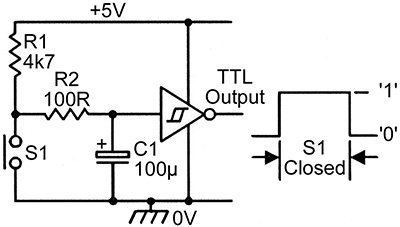
FIGURE 6. Switch-debouncing input interface.
Here, C1 charges — with a time constant of about 10 ms — via R1-R2 when S1 is open and generates a logic-0 output via the TTL Schmitt inverter. When S1 is closed, it rapidly discharges C1 via R2, driving the Schmitt output high. The effects of any switch-generated bounce signals are eliminated by the circuit’s 10 ms time constant, and a clean TTL switching waveform is thus available at the Schmitt’s output.
Figure 7 shows a circuit that can be used to interface almost any clean digital signal to a normal TTL input. Here, when the input signal is below 500 mV (Q1’s minimum turn-on voltage), Q1 is cut off and the inverting Schmitt TTL output is at logic-0. When the input is significantly above 600 mV, Q1 is driven on and the Schmitt output goes to logic-1. Note that the digital input signal can have any maximum voltage value, and R1 is chosen to simply limit Q1’s base current to a safe value.
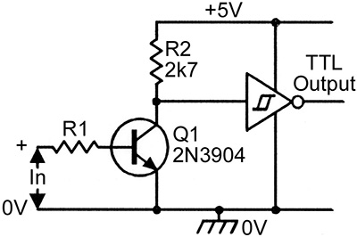
FIGURE 7. Transistor input interface.
Figure 8 is a simple variation of the above circuit, with the transistor built into an optocoupler. The circuit action is such that the Schmitt’s output is at logic-0 when the optocoupler input is zero, and at logic-1 when the input is high. Note that the optocoupler provides total electrical isolation between the input and TTL signals.
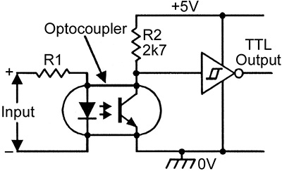
FIGURE 8. Optocoupler input interface.
Finally, Figure 9 is another simple circuit variation, with the basic digital input signal fed to Q1’s base via the R1-C1-R2-C2 low-pass filter network. This filter eliminates high-frequency components and can thus convert very dirty input signals (such as those from vehicle contact-breakers, etc.) into a clean TTL format.
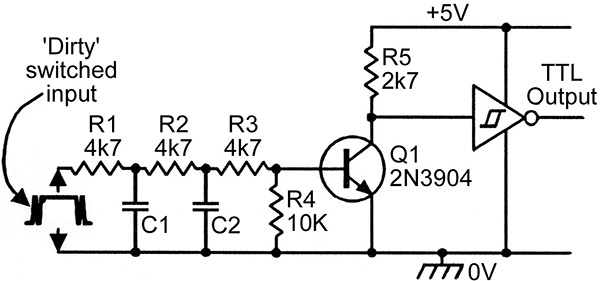
FIGURE 9. “Dirty-switching” input interface.
Output Interfacing
Most TTL ICs have normal totem-pole output stages, but some of them have modified totem-pole outputs with three-state (tri-state) gating. A few TTL ICs have open-collector totem-pole output stages. Note that normal totem-pole outputs should not (except in a few special cases) be connected in parallel. TTL open-collector outputs can be connected in parallel, however, and tri-state ones can be connected in parallel under special conditions. Basic ways of using open-collector and tri-state outputs will be described in a future digital ICs article.
A normal totem-pole output stage can source or sink useful amounts of output current, and can be used in a variety of ways to interface with the outside world. A few simple examples of such circuits are shown in Figures 10 to 17. Figure 10 shows a couple ways of driving LED output indicators via non-inverting TTL elements.
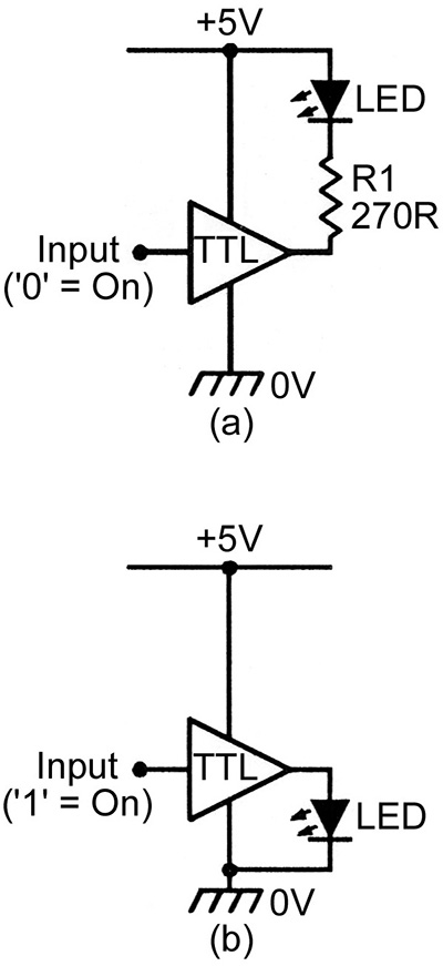
FIGURE 10. LED-driving output interfaces, using non-inverting TTL elements.
Note that a normal TTL output can sink fairly high load currents (typically up to 50 mA in an LS device), but has an internally limited output sourcing ability. Thus, the LED current must be limited to a safe value via R1 if it is connected as in Figure 10(a), but is internally limited in Figure 10(b). Figure 11 shows alternative ways of driving LEDs, using inverting TTL elements.
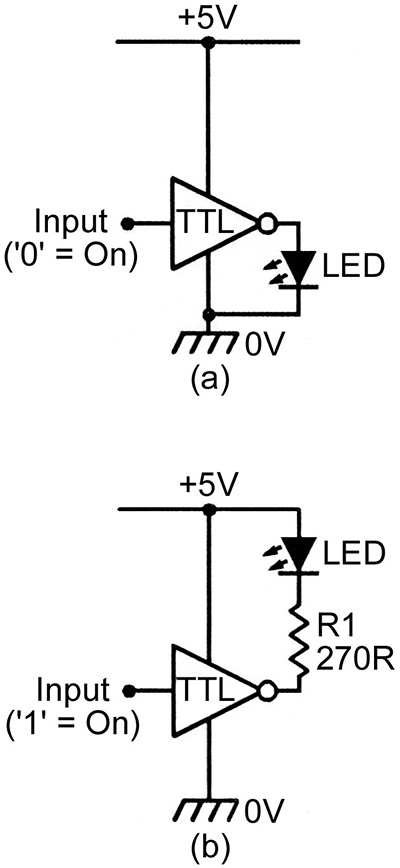
FIGURE 11. LED-driving output interfaces, using inverting TTL elements.
Figure 12 shows two current-boosting load-driving output interface circuits, in which the load uses the same power supply as the TTL circuit.
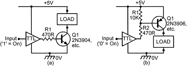
FIGURE 12. Current-boosting, load-driving output interfaces.
In Figure 12(a), NPN transistor Q1 is cut off when the input of the non-inverting TTL element is at logic-0, and is driven on via R1 when the input is at logic-1. The reverse action is obtained in Figure 12(b), where PNP transistor Q1 is pulled on via R2 when the input is at logic-0, and is cut off via pull-up resistor R1 when the input is at logic-1.
Figure 13 shows two output interface circuits that can be used to drive loads that use independent positive supply rails.
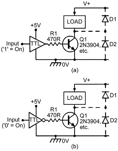
FIGURE 13. Output interface to a load with an independent positive rail.
Q1 is turned on by a logic-1 input in Figure 13(a) and by a logic-0 input in Figure 13(b). If the external load is inductive (such as a relay or motor), the circuits should be fitted with protection diodes, as shown dotted in the diagrams.
Figure 14 shows two optocoupled output-interface circuits that can be used to drive loads that use fully independent DC power supplies. T
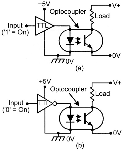
FIGURE 14. Optocoupled output interface.
he load is turned on via a logic-1 input in Figure 14(a) and by a logic-0 input in Figure 14(b). Note that the optocoupler input (the LED) could alternatively be connected between the +5-V rail and the TTL output via a current-limiting resistor, using the same basic connections as in Figure 10(a) or Figure 11(b).
Figure 15 shows an output interface that can be used to control a low-power lamp or similar resistive load that is driven from AC power lines and consumes no more than about 100 mA of current.
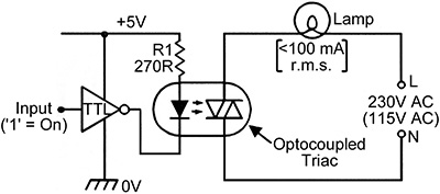
FIGURE 15. Output interface to a low-power AC lamp via an optocoupled triac.
This circuit uses an optocoupled triac. These typically need an LED input current of less than 15 mA and can handle triac load currents of up to about 100 mA mean (500 mA surge) at up to 400 V peak.
Note that optocoupled triacs are best used to activate a high-power slave triac, which can then drive a load of any desired power rating. Figures 16 and 17 show two such circuits.
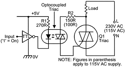
FIGURE 16. Output interface to a high-power non-inductive AC load.
The circuit in Figure 16 is suitable for use with non-inductive loads, such as lamps and heating elements. It can be modified for use with inductive loads, such as motors, by using the connections of Figure 17.
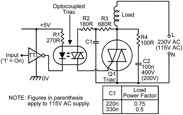
FIGURE 17. Output interface to a high-power inductive load.
In Figure 17, R2-C1-R3 provides a degree of phase shift to the triac gate-drive network, to ensure correct triac triggering action. R4-C2 forms a snubber network, to suppress rate effects.
Logic-Family Interfacing
It is generally bad practice to mix different logic families in any system, but on those occasions where it does occur, the mix is usually made between TTL and CMOS devices that share a common 5 V power supply. In this case, the form or necessity of any interfacing circuitry depends on the direction of the interface and on the precise sub-families that are involved. Figures 18 to 21 show the four most useful types of interface arrangement.
The output of any TTL element can be used to drive any normal CMOS logic IC (including some sub-members of the 74-series) by using the connections shown in Figure 18, in which R1 is used as a TTL pull-up resistor to ensure that the CMOS consumes minimal quiescent current when the TTL output is in the logic-1 state.
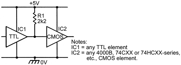
FIGURE 18. TTL-to-CMOS interface.
Standard 4000B-series and 74CXX-series CMOS elements have very low fan-outs, and can only drive a single standard TTL or LS TTL element, as shown in Figures 19 and 20.
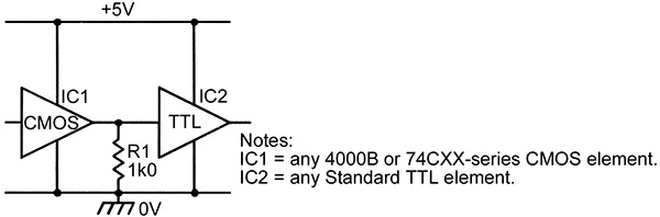
FIGURE 19. CMOS-to-Standard-TTL interface.
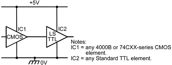
FIGURE 20. CMOS-to-LS-TTL interface.
74HCXX-series (and 74ACXX-series) CMOS elements, on the other hand, have excellent fan-outs, and can directly drive up to two standard TTL inputs, 10 LS TTL inputs, or 20 ALS TTL inputs, as shown in Figure 21.
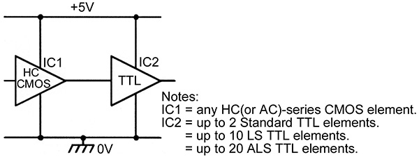
FIGURE 21. HC-CMOS-to-TTL interface.
In cases where the TTL and CMOS ICs use individual positive supply rails (5 V for TTL, 3-18 V for CMOS), an interface can be made between the two systems by using a direct-coupled NPN transistor as a level shifter between them, as shown in Figures 22 and 23. (These simple circuits may need some refining if they are to be used at frequencies above a few hundred kHz.)
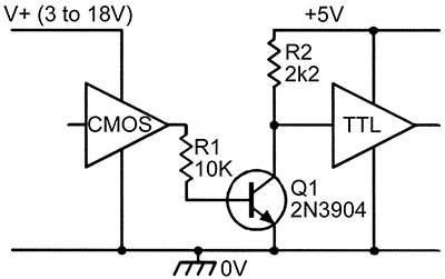
FIGURE 22. CMOS-to-TTL interface, using independent positive supply rails.
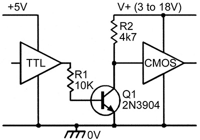
FIGURE 23. TTL-to-CMOS interface, using independent positive supply rails.
Finally, note that if the TTL element has an open-collector, totem-pole output, a direct interface can sometimes be made between the TTL output and the input of an individually-powered CMOS element, etc. The basics of this technique will be described in our next installment of this four-part mini-series. NV