With TJ Byers
IGBT Basics
Question:
Years ago, while attending the University of Illinois, I ran a photo service taking fraternity/sorority dance pictures and portraits to make spending money. After graduating, I gave up photography but held on to my old Grafles Stroboflash equipment. Now with more time on my hands, I decided to take up photography again. My wife bought me a new Nikon for Christmas and I was off ... ’til I discovered that the 225 V batteries for each strobe unit (I have six) cost $200 each! Being the “evil genius” that I fancy myself, I decided to build my own strobes running off AC mains using the old flashtubes.
After researching the new technologies, I decided to go with IGBT transistors instead of SCRs because they allow me the most control, letting me operate them from a PIC or Stamp microcontroller. Here is my problem: The info on IGBTs out there is Greek to a person with a degree in ME not EE. Can you explain them in terms I can understand?
— Albert J Sanowskis
Reddick, FL
Answer:
The IGBT (insulated-gate bipolar transistor) is basically the marriage between a MOSFET (metal-oxide field-effect transistor) and a bipolar transistor. It has the output switching and conduction characteristics of a bipolar transistor, but is voltage-controlled like a MOSFET. Generally, this means it combines the high-current-handling capability of a bipolar part with the ease of control of a MOSFET.
The structure of an IGBT die is similar to an N-channel MOSFET, with one added junction. This added junction effectively becomes the collector of the PNP bipolar transistor, which is driven by the N-channel MOSFET. Besides the PNP transistor, there is an NPN transistor that forms a Darlington pair (Figure 1), thereby giving the IGBT its bipolar output characteristics.
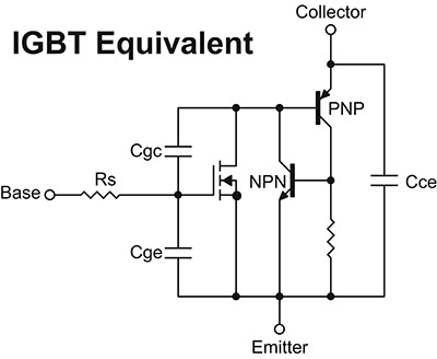
FIGURE 1.
This variation between MOSFET and IGBT is enough to produce some clear distinctions as to which device serves which applications better. Clearly, the IGBT is the choice for breakdown voltages above 1,000 V, while the MOSFET is better for breakdown voltages below 250 V. When the breakdown voltage is from 250-1,000 V, choosing between them is a very application-specific task in which cost, size, and speed must be taken into account.
IGBTs have been the preferred device under the conditions of low duty cycle, low frequency (less than 20 kHz), and high output power in excess of 5 kW. Typical IGBT applications include motor control, UPS power supplies, high-current welding, and low-power lighting with operation frequencies below 100 kHz.
MOSFETs are preferred in applications where high-frequency operation above 200 kHz is required, with wide line or load variations, long duty cycles, low-voltage applications (less than 250 V), and low output power (under 500 W). Typical MOSFET applications include switching power supplies and battery charging. Of course, nothing is as easy as it seems. Tradeoffs and overlaps occur. See Table 1 for a direct comparison of bipolar, MOSFET, and IGBT.
The front end of the IGBT is essentially identical to that of the MOSFET, and should be treated accordingly. That is, you have to respect the Miller charge effect and the plateau that the transistor must go through to become fully saturated (see “MOSFET Basics” above). Figure 2 shows the gate characteristics for a typical IGBT device in the switch-on mode. Notice that the charge is measured in coulombs (QG). Doing the math — C = QG / E — we calculate that Cg is 0.01 µF.
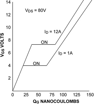
FIGURE 2.
Enter Rs — the gate series resistor. This resistor determines the time it takes for the transistor to go from full OFF to full ON by restricting the flow of current to the input capacitance using the formula t = 5(RC). The smaller Rs is, the faster the transistor will switch on. It also reduces external noise that can falsely trigger the transistor. On the other hand, large inrush currents can stress the gate junction by momentarily causing the gate voltage to exceed VGE thresholds. But as Rs increases, so does the turn-off time. This is great if you want soft turn-off, but not good for flyback applications. As you can see, a proper gate driver and Rs value is critical to the success of your design. Most datasheets show the value of Rs they used to generate the parameters and test results listed. This is a good place to start.
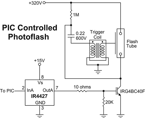
FIGURE 3.
Back to your specific application of building a flashtube controller, I suggest the circuit in Figure 3. For the driver, I chose the IR4427 (Figure 4) because it can sink and source up to 1.5 A — and is ideally suited for
driving MOSFET and IGBT transistors.
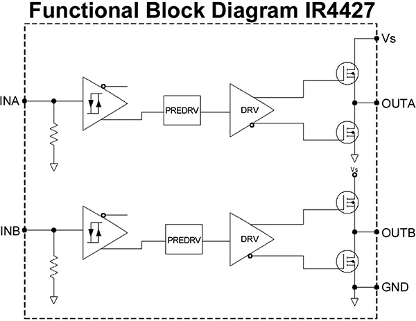
FIGURE 4.
Taking the value of Rg from the IRG4BC40F datasheet, and using conventional IGBT input design, I came up with the 10-Ω series and 20-kΩ parallel resistor input combination. When a positive pulse is applied to the input of the IR4427, it triggers the IGBT — which, in turn, discharges the 0.22 µF cap through the trigger coil and fires the flashtube. Notice that the IR4427 has two drivers in its package, which means it can drive two flashtubes or be paralleled for more drive current. Providing the 320-V charging voltage and programming the PIC is up to you.
Can’t get enough MOSFET stuff? Continue this thread with “You Take The High Road ...”
Comments