Does anyone still make oneoff circuit boards at home? What methods are being used by hobbyists and where do you get supplies?
#03204
Alvaro Collazo
Gulfport, MS
Please log in to post an answer.
Answers
For prototypes I use Press-n-Peel. You laser print the pattern to the PNP then use a clothes iron, or better, a laminating machine to bond it to the copper side of the board. Peel the PNP off the board and etch it. Clean the residue off the board then drill as needed and assemble it.
This from my post on forum.nutsvoltscom Re: Making PCBs at Home Post by Lenp » Wed Sep 02, 2020 3:43 pm
- Photocopy, or laser print the artwork onto overhead projector film unless you already have reverse artwork.
- If you use the the projector film, turn it over as needed to get a reverse image on the blue Press N Peel transfer film.
- You may have to tweak the copier’s toner for a dark image, and it might be a just a bit off scale, if that matters much.
- The circuit board should be bigger than the PCB pattern to help fix any misalignment problems.
- Clean the circuit board with something like a Scotch Brite pad, and wash well with alcohol to get rid of any oils or finger prints.
- Hold the board by it’s edges and align the PNP pattern on the board properly, taping one edge to keep it in place
- If you have a pouch laminator, run the board and film, with the taped edge leading,through using a pouch carrier.
- Without a laminator, you can iron it on with a clothes iron. Put a few sheets of paper on top of the film to keep it from slipping.
- The toner on the film will get sticky when hot, and bond to the board. Allow the board to cool, or rinse in cold water.
- If the board is missing a bit of a trace, choose to do it over, or repair the damage with a Sharpie marker.
- Acetone will remove the pcb pattern from the board so it can be reused if necessary, but clean it again.
- Etch in any available etchant. (I prefer amonium persulfate since it is less mess.)
- After etching, I leave the PNP pattern on until the drilling is done, then clean it with acetone but you can clean it first if desired
Overhead film is available online and maybe the big box office stores still carry it (who uses overhead projection any more?). PNP Blue film comes with an instruction sheet and it is available online, and from several electronic suppliers that also supply the copper board and etchants. Look online, it’s there as well as several videos showing the process.
This PNP process is great for a not too complex board prototype, but not for quantities. You can have a board from artwork to drill in an hour, correct your mistakes and go again without waiting for a board house turnaround and cost.
Good luck!
Len Powell
Finksburg, MD
I quit doing that when I spilled a gallon bottle of Ferric Chloride in the garage. A friend of mine was recently making some, but the materials are getting hard to get. Besides, ordering small quantities from China is way cheaper than buying the board and chemicals.
Richard Cox
Thousand Oaks, CA
The two most common methods I'm aware of are toner transfer and Photosensitive Dry Film. Most people seem to have much better luck with one or the other. I was never able to get toner transfer to work so I use UV film. The supplies for either are available at the usual sources (Mouser, Digikey, Jameco, Amazon, etc). There are a number of articles and videos on the web which describe the process better than I can.
Basically, a UV sensitive film is applied to the PCB, then a transparency is laser printed to overlay it. The areas blocked by the design are those which will be etched away (the print is a negative). The board is dipped in a developer for a couple minutes before it's washed with water. There are a number of echants, but the most common in hobby use is probably ferric chloride. If you use it, please check handling and disposal methods.
You may want to look at PCB prototyping services. Several advertise in Nuts & Volts. For $25-30 you can get 5 boards, 6 mil spacing, drilled, vias, masked, and screened, at your door in a week or so. Honestly, this is probably the way to go, unless you need faster turnaround. Or just wanna (a valid reason in itself!). It is very important to closely check the design rules.
Another possible option is CAD/CAM milling. However, I'm not aware of affordable equipment which has enough precision. I haven't looked in a while, so this may have changed.
Jay C
Louisiana
In the past, I designed and produced many circuit boards using several methods. By far, the best way to produce circuit boards is to just send the files to a company on the web and have them make them because if your time is worth anything, it is cheaper. However, if you insist on doing it yourself, you can etch them or mill out the unwanted copper, leaving the circuits that you want.
Milling works much better because circuit design software can produce files which can be converted to a program that runs on an othermill home router. It’s likely that other home routers can also be used, but the two people that I’ve seen do it used othermills. These machines are very popular at Makerspaces and school shop classes, etc. Adafruit uses this method to produce all of their one of a kind circuit boards for production testing their products.
This process starts with getting and learning KiCad software, which is free. YouTube has many videos on learning KiCad and Lady Ada often shows how she designs products for Adafruit using KiCad on her “Desk of Lady Ada” YouTube series. Watching this series from the beginning is suggested for anyone learning electronics.
After the KiCad design is done, it’s a matter of contacting the owner of a usable milling machine or sending the files to a board maker. The Hackaday guide: Why Etch A PCB when You Can Mill is suggested reading.
If you are dead set on etching your own boards, you can get several kinds of etchant from Amazon as well as some blank boards. However, a search of the web will likely show several other sources.
Forget any Ferric Chloride based etchant as it’s nasty stuff and works much slower than the better product Ammonium Persulfate, which stays clear enough to see how the process is coming along. You’ll also need a way to time the exposure of the boards and the right kind of lamp. I would suggest making the final board pattern on clear film that can then be taped over the copper clad board and exposed.
The other way to do it is to draw the pattern directly onto the circuit board with a “resist pen,” but it’s very hard to do an accurate job that way.
The transparent film can be printed on certain printers if the correct film stock is used, however getting the size of the image correct to produce the correct size printout might be tricky. We always drew everything 4 times bigger on graph paper and then had a photo shop reduce it 4:1 and print it on clear film.
Good Luck
Dale Freye
Grand Haven, MI
With the rise of the cheap board manufactures that can provide you a professional board for just a few dollars, this is something of a lost art. I still make my own boards most of the time. The time I have to bring my ideas to life is pretty limited and when I have a good idea I want execute on it right away.
When it comes to making my boards, I would call myself a jack of all trades and master of none. I use a few different methods depending on the complexity of the board and how polished I want the final product to be.
My go to method is photoresistive film and that produces the best output for me. Autodesk Eagle is my tool of choice for laying out my board, printing that output on laser printer transparencies and using a cheap laminator from the local big box store, a cheap light box and photoresistive film from eBay and I can lay down my artwork in about 30 minutes. There are plenty of Internet resources on how to do this online and it works great.
Etching is where the real issues are with making your own boards. It’s messy and dangerous. after all you are dealing with chemicals strong enough to erode metals. I used ferric chloride for years, and it gets the job done, but it’s slow and extremely messy. If you ever spill any, plan on the brown stain left behind to be there forever.
For the past 5 years or so I’ve been using muriatic acid (Hydrochloric Acid) and peroxide for etching my boards in a 50/50 mix. It is super effective and I can run to the local hardware store to grab a gallon, but it is has quite a few real hazards.
First and foremost it gives off chlorine gas so is has to be done outside and away from others and you must always use eye and breathing protection.
Secondly, anything within reach of the fumes made of ferrous metal will rust almost instantly. Both ferric chloride and muriatic acid like to be warm and agitated to work best. I made a simple servo driven device controlled by an arduino to rock the container back and forth and that speeds up the process greatly.
Drilling is next in line and again I have a few methods I use. My primary is just a simple micro drill press and hours of doing my best to hit the center of the pads. Drilling after etching allows you to use the raised copper pad to guide the drill bit.
Lately I have been working on a good technique for using my cheap 3018 CNC router to do this more effortlessly. By etching some alignment marks on two corners of the board I can pin the board down to the waste board on the CNC and let it do all the hard work. So far it is hit and miss but when it works it does a great job.
inally there is making it look good with some solder mask. While it is mostly for aesthetics for me, it does have a real purpose to keep your copper traces from oxidizing. I nearly always use Dynamask film.
Since I usually do photoresist film on my boards, and Dynamask works just like it, I have the tools out and on the bench anyway. Occasionally I use the liquid mask that you can order on Amazon or eBay, and it works, but it just doesn’t product the quality I get out of Dynamask.
So there it is, when you add all the time up and include cleanup afterwords, for a simple board you have used up the better part of a day. Is it worth it? No it’s not, considering the low cost of ordering professional quality boards now.
Will I keep doing it? Absolutely. While it is a ton of work and mess there is just something about it I really enjoy.
After I do my prototype on my hand made board and work out the details, I will get the real deal from a PCB service but the ability to test out an idea on a board the same day the idea hits you is awesome.
David Carter
Frankfort, KY
My son has recently become a model train enthusiast and asked me how to control multiple trains on the same track. Is it possible and how would one go about building a controller?
#03202
Paul Sills
Grand Rapids, MI
Please log in to post an answer.
Answers
To do what you want you will need to use the system called DCC. To see an explanation of how it works, see Practical Electronics, Jan 2021 where they show (on page28) how the voltage going to the tracks is encoded with digital control information as well as being the power source for all the trains and other equipment controlled by the system.
I suggest reading the magazine at a book sellers place while enjoying a drink because the magazine costs $12. I would not suggest building the circuit when similar factory built units are available, because the blank circuit board is 12 Pounds each plus VAT and shipping from GB.
Amazon lists a DCC controller called NCE PROCAB #5240010 which looks like a large TV remote with a display that can control your whole layout. This equipment is not cheap.
A review of the Bachmann HO scale "ChargerSC-44" diesel locomotive with AmTrack Cascades 1400 paint as shown in Model Railroad News, May 2021 is pretty favorable. It is part #67904 MSRP $469 from Bachmann Trains. 800 356 3910 https://bachmanntrains.com Also check out Walthers 800 487 2467 https://www.walthers.com for some less expensive models.
I hope this will be useful and get you started in the right direction.
Dale Freye
via internet
You and your son are in luck, controlling multiple trains on the same track is a problem already solved with Digital Command Control (DCC). The beauty of using DCC is that the National Model Railroad Association (NMRA) has a series of electrical standards that define the signal between the transmitter (known as the command station) and the receiver (known as the decoder). The NMRA published the first of the DCC standards (see https://www.nmra.org/index-nmra-standards-and-recommended-practice) 20 years ago, so these standards are well established and stable.
There are multiple manufactures of DCC systems. Each system has a command station to create the signal and a booster to amplify the signal that is sent out over the rails. The manufacturers differ in the manner they input the user signal into the command station, via a throttle (also called a cab), since this in not covered by the NMRA standard.
A decoder is placed in each locomotive. There are also multiple manufactures of decoders. Compliance with the NMRA standard allows any manufacturer’s decoder to correctly interpret any manufacturer’s DCC signal. Should you wish to purchase a “starter set”, my advice is to avoid over-researching, since given the time-honored DCC standards, there are no “bad” systems on the market. Rather, find a neighbor, friend, or local model railroad group that is willing to assist, then purchase whatever DCC system they are using.
Being a Nuts and Volts reader, you have other options to explore. Type “DYI DCC” your browser’s search. You will find numerous variations using an Arduino or Raspberry Pi to provide the signal while an old computer running a Java-based cross-platform program, JMRI (see https://www.jmri.org), provides all interface. If your son’s locomotives do not have a manufacture installed decoder, he will be able to learn advanced soldering skills.
In summary – Jump into Digital Command Control and get much more out of the hobby than you and your son originally expected.
Dick Schwanke
Model Train Controller
There is a model train system called DCC where electronics in the train engine are controlled by a wireless remote control. Multiple trains can be controlled for speed, lights, horns, smoke etc. Visit a good hobby shop that has a train section or search online.
Richard Cox
Thousand Oaks, CA
What you're probably looking for is DCC (Digital Command Control) technology. I use the Digitrax system for my layout. There are also a few DIY projects out there: https://dccwiki.com/DCC_Projects.
The simplest explanation for this is each loco has a unique decoder embedded inside. The tracks are always energized and commands are sent along the tracks from the controller, causing the recipient loco to execute that command. Good luck!
Michael Picco
Placerville, CA
How do I calculate the number of turns for both the primary and the secondary windings of a transformer?
#03203
Opeyemi
Ibadan, Oyo
Please log in to post an answer.
Answers
The main problem with transformer design is the determination of the minimum number of turns for the primary. With too few turns, the transformer will overheat. Too many turns is only a problem if the turns will not fit within the “E-I” core windows.
We also need to determine what size of wire to use in the windings. With the aid of information extracted from Reference 1, we can design a power transformer having a 50 degree C temperature rise above ambient.
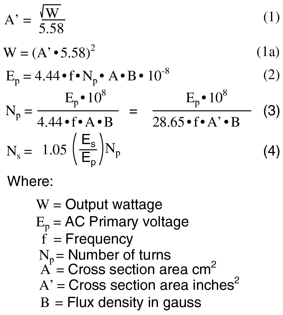
Figure 1
Use Equation 1 Figure 1 to estimate the size of the silicon steel laminated core required, given the wattage of your application. For example, a 12V 2.6A = 31.2W transformer requires a core with a cross section of one square inch (sqrt (31.2))/5.58 = 1.0. If you already have a core, multiply the height and width of the center leg to compute the cross section area as in Figure 2. Use Equation 1a to calculate the wattage rating of your core. The area will be A’ in Equation 3 if you measure in inches; A if measured in cm.
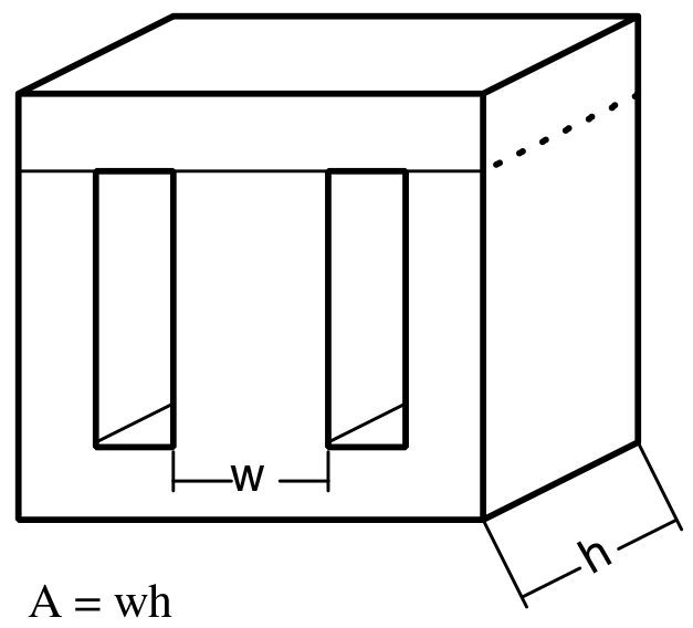
Figure 2
Equation 2 from Reference 1 was solved for Number of turns Np as Equation 3 The right-hand side of Equation 3 has a conversion factor applied to accept A’ in square inches instead of A in square centimeters. For our example as a 120 VAC 60 Hz transformer, set Ep=120, F=60, and A’=1.0. Consult Figure 3 for the recommended flux density B in gauss for the wattage of 31. Set B = 13,000. Equation 3: Np = 120(10e8) / (28.65)(60)(1.0)(13,000) = 537 turns.
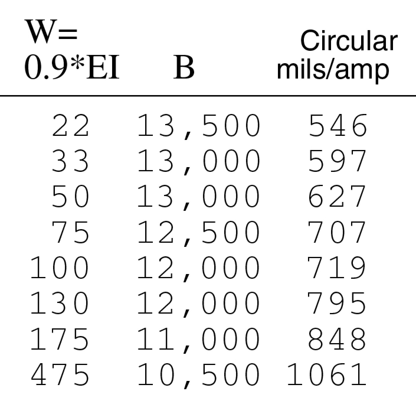
Figure 3
Note that Equation 4 for Ns number of secondary turns has a 1.05 multiplier to account for winding resistance loss.
Continuing with our example, Ns = (1.05)(12/120)(537) = 56 turns.
The next problem is to determine what size wire to use for the primary and secondary windings. The size of wire depends on the wattage of the transformer. Small low-watt transformers dissipate heat more readily; thus, can get by with smaller wire size. Our 12V 2.6A = 31.2W example requires 597 circular mils of wire area per amp of current according to Figure 3. We need 597 * 2.6 = 1552 circular mils for the secondary wire. Looking up Reference 2, we find that 18 AWG wire has 1,624 circular mils of area; thus, 18 AWG for the primary. Since our primary/secondary turns ratio is 10/1, the primary current will be one tenth the secondary current (1/10)*2.6A = 0.26A. As with the secondary, we need 597 circular mils per amp. We need 597 * 0.26 = 155 circular mils for the primary. Consulting Reference 2, we find that AWG 28 has 160 circular mils for our primary winding.
Though I have not encountered any difficulty fitting the windings within the window space, you can estimate how much space will be required by consulting Reference 3 for turns per inch of a layer, and Reference 2 for wire diameter to estimate layer height. Use 90% of the turns per inch, 110% of wire diameter for layer height. Allow for thickness of the form on which the windings reside, allow for ends of the form, and insulation between the primary and secondary. Small diameter wire may require thin paper between each layer.
A complete re-wind of a transformer is only applicable to “E-I” cores that can be disassembled. Welded or epoxied cores cannot be disassembled. However, a few turns of a high-current secondary wire may be threaded through the window. According to YouTube videos, the secondary of a microwave oven transformer may be hacksawed and replaced with a few turns of heavy gauge wire.
Rather than a complete re-wind, consider re-using an existing primary by applying a custom secondary. Count the turns unwound from a known voltage secondary. Calculate turns per volt to aid in determination of the custom secondary turns.
- Reference Data for Radio Engineers, 4th Ed,1956, ITT, pp 275.
- Copper wire gauge table, www.ibiblio.org/kuphaldt/electricCircuits/Ref/REF_3.html#cuwire.tbl.
- AWG gauge vs. turns per inch, www.ibiblio.org/kuphaldt/electricCircuits/Ref/11099.png.
Dennis Crunkilton
Abilene, TX
I sometimes see a diode placed across relay contacts backwards. Can someone explain the purpose of this and when it’s necessary and when it’s not and why?
#06194
Jürgen Abend
Pleasanton, CA
Please log in to post an answer.
Answers
All but one of the answers here didn't answer the OP question, which was about a diode across the CONTACTS, not the coil. As the one answer that addressed the issue indicated, the reason is to suppress arcing across the relay CONTACTS when the coil is de-energized (particularly if the contacts are connected to anotrher inductive load).
Jay Jaeger
Madison, WI
It is used to protect the components of the circuit from burning out from a release of the induced voltage when the relay is turned off. The energy stored in the magnetic field of the relay coil is now released and the voltage can get quite high and case a spark. If high enough, this can cause damage, but even if it’s a low voltage, it can cause RFI and cause a circuit to misbehave. This diode has a number of names, but I like calling it the flyback diode.
Example: I once built a 8080 based microcomputer and programed it to turn lights on and off in the house when we were on vacation. But, it was always glitching, the program would get lost and hang up. Until I realised I was not using any flyback diode on all the relays. Once these were installed the RFI noise was removed, or at least reduced enough, so that the computer would not lose its place in the program and all worked fine from then on.
Aside: A flyback transformer where this flyback voltage is put to good use, see: https://en.wikipedia.org/wiki/Flyback_transformer
I looked this up to find more for you, check out these web pages: This is a good explanation: https://resources.altium.com/p/using-flyback-diodes-relays-prevents-electrical-noise-your-circuits
Here’s a good article on Wiki: https://en.wikipedia.org/wiki/Flyback_diode
Phil Karras KE3FL
The diode is called a flyback diode. The purpose is to dump the energy from the relay coil when it is disconnected from power. The coil acts as an inductor and when the power is disconnected, as when a transistor turns off, the current can not change instantly. This results in the voltage across the coil spiking to try and keep the same current flowing.
The diode lets the current flow thru it when the power is turned off keeping the inductive kick from destroying the transistor. No current flows thru the diode when the coil is energized because it is reverse biased then.
Some relays have the diode built in and do not require an external one. If you replace the relay and there was no diode across it the old one may have had an internal diode. If your replacement does not have a built in diode you should add one externally.
Larry G Nelson Sr
Webster, MA
When a voltage is removed from the relay coil, the magnetic field collapses, inducing an inverse pulse to flow. This inverse pulse can damage transistors and - more easily - ICs. The diode sorts this pulse so that it doesn’t damage any sensitive components.
If you are controlling a relay with any silicon device - e.g. transistor, IC, etc - you probably need to use a diode (called a snubber diode, by the way). If you are controlling the relay directly, say with a switch, then you don’t really need it.
Derek Tombrello
Shelby, AL
When the energizing contacts of a relay (or any inductor) open, the collapsing magnetic field forces the current to keep flowing. If the applied voltage was large and the coil is large enough, a substantial voltage will build up across the ends of the coil. If the voltage is very large, it will cause damage to the circuit. The diode is to short the voltage and prevents damage.
Lance Corey
Santa Ana, CA
Not across the contacts, but across the coil. It is called freewheeling or flyback diode. It provides a path for the high voltage created by the collapsing magnetic field when current is cut off. Otherwise the high voltage can destroy the driving circuit. Also used across solenoids and sometimes DC motors.
Richard Cox
Thousand Oaks, CA
Mr. Abend asks about diodes placed backwards across relay contacts. NOTE that this technique is applicable only in DC circuits.
The diode is called a “snubber” and it serves to protect the relay contacts from overvoltage in inductive circuits. Relay contacts in DC circuits are subject to sparking as they open when they control an inductive load. This opening can occur intentionally, or can occur during contact closure due to contact bounce. Examples of inductive loads include motors, solenoids, or other relay coils.
Current and voltage in an inductive circuit are related by Faraday’s Law, one form of which is V = -L di/dt. It states that the rate-of-change of current (amperes per second) in an inductor is proportional to the voltage applied across the inductor and inversely proportional to its inductance (henries). The minus sign indicates that the inductor resists a change in current by opposing the applied voltage.
Consider a voltage applied across an inductor through a set of relay contacts: At the instant of contact closure, load current is zero. As time advances, and dependent upon the load inductance, the current through the inductor will increase at a constant rate determined by the ratio V/L. At some point, the inductor will saturate — i.e., it cannot be magnetized further — whence the limiting current will then be governed by the winding resistance.
Now consider what happens when the relay contacts open: The magnetic field in the inductor immediately begins to collapse, and as it does so, it will attempt to drive current back into the voltage source. But since the voltage source no longer exists — we have an open circuit — there is nothing (other than the inductor’s winding resistance) to limit the magnitude of the voltage induced, and this kickback voltage will therefore appear across the relay contacts that are in the process of opening — contacts that have, in fact, barely moved from their closed position. The polarity of the kickback voltage is opposite to that of the original voltage that was used to energize the inductor. The kickback voltage creates a spark that degrades the contact surface, and over time, this sparking can cause contact failure.
A backwards diode connected across the relay contacts will switch into conduction when kickback voltage is applied. In this case, the decreasing rate-of-change of inductor current will be governed by the inductor winding resistance (ignoring the forward voltage drop in the diode).
Practical examples: An inductor having an inductance of 1 henry and a winding resistance of 1000 ohms, energized by a 25-volt source. The rate-of-change of increasing current in the inductor will be 25 amperes per second (25 milliamperes per millisecond) and the limiting steady-state current will be 25 milliamperes — which will be attained in about one millisecond.
When the voltage source is removed, as by opening a relay contact protected by a snubber diode, the initial value of the inductor current will be the same as its limiting value earlier — 25 milliamperes. The decrease in inductor current over time (t) is an exponential function of winding resistance (R) and inductance (L) proportional to e (exp -tR/L).
When the switching device is a transistor, the snubber diode serves to protect the transistor from destruction due to the imposition of kickback overvoltage.
Peter A. Goodwin
Rockport, MA
More often the diode is placed across the coil such that it is reverse biased. Its purpose is to absorb the counter EMF when the coil is de-energized . When the relay coil is energized it stores energy in its magnetic field. When the current is turned off that magnetic field reverses and tries to keep current flowing in the circuit. However, since the path is open that energy must dissipate. The energy can produce a rather high-voltage spike. This is how the Kettering ignition system works in early automobiles spark generation.
Since in most small electronics we do not want that high voltage to damage components the diode across the coil shorts out that reverse Electro-Magnetic-Field (EMF) and thus saves delicate components. You may find a diode or other suppressing component across contacts for the same reason. i.e. To prevent a spark which would shorten the contact life or damage other components.
In the automobile ignition system there is usually a capacitor placed across the points in the distributor. The ignition coil produces the spark when the contacts open because the magnetic field collapses sending that energy to the spark plug(s). I hope this helps you understand a little bit more about inductance in coils.
William B Runyon Sr WF4R
Chesapeake, VA
When a relay (or other) coil is de-energised, the stored charge can create a substantial back e.m.f. amounting to several hundred volts. This voltage can damage delicate components (FETs etc.) in the ciruit.
The reverse connected diode will clamp this voltage to 0.6 or 0.7 volts for a silicone diode. This limits any fast going high voltage spike in the circuitry.
Paul Reckless
Aylesford, Kent,
The problem the diode is solving occurs when the current flowing through the relay coil is switched off. This on-to-off transition is relatively fast and the collapsing magnetic field (the field generated to actuate and hold the relay in its switched condition) generates a very high reverse voltage across the relay coil. The relay coil current is usually switched by a switching-transistor.
This reverse voltage can easily exceed the capacity of the switching-transistor’s reverse-breakdown voltage and, thus, destroy the transistor. To solve the problem, the backwards diode provides a forwards path for the collapsing current to cycle back through the relay, and thus the backwards current flow dissipates within the relay.
Greg Gentile
San Francisco, CA
A diode is used on relays to keep back EMF from taking out the device driving the relay when power to said relay is turned off. When power to a coil goes off, the magnetic field collapses. This causes very high voltages and currents on the relay coil. They can go backwards into the drive circuit, damaging the active device. They are used where damage is very likely. Hope this helps.
Robbie J
Green River, WY
The coil of a relay is a fairly large inductor. Inductors store energy in a magnetic field that builds up around the coil when current if flowing through the coil. If the current is turned off suddenly the magnetic field collapses and "induces" voltage in the coil, just like a generator. The stored energy has to go somewhere and the induced voltage tries to keep the current flowing in the same direction.
The voltage will continue to rise with a polarity opposite of what had been applied. That means the end of the coil that had been connected will generate a voltage much higher than, and added to, the supply voltage at the other end of the coil. That voltage can easily rise to a level high enough to damage the circuitry. The diode placed "backward" across the coil provides a path for that current. It effectively shorts out the voltage induced in the coil and allows the stored energy to dissipate in the diode and the wiring without reaching dangerous levels. The diode should be rated somewhat higher than the supply voltage and should be able to handle at least the same amount of current as the relay coil.
When is it necessary? The full answer requires quite a bit of math and physics but the short, simple answer is anytime an inductive device is switched off and on. It applies not only to relay coils, but also to motors, solenoids, and any other type of devices with coils/inductors. In some cases the switching circuit will have protective diodes built in. For instance, the ULN2803 darlington array IC is intended for driving such loads and has the diodes built in. The L293D (D for Diode) stepper motor driver / dual H bridge IC also has protective diodes built in.
William Cooke
Adams, TN
The diode is there to protect any solid state device driving the relay. The current flow through the energized coil creates a magnetic field around the coil. When switched off the collapsing field results in an instantaneous polarity change in voltage across the coil. Without the diode this voltage can become quite large exceeding the voltage rating of the switching device. The changed polarity of the voltage induced into the coil forward biases the diode limiting or clamping the voltage rise to around 0.7 volts.
Sometimes referred to as a snubber diode or snubber circuit. Sometimes an RC circuit is used in this fashion but diodes have become more common. Some 12 V automotive relays include this diode internally, others do not. I would not replace one with a diode with one without. The diode is "backwards" because we do not want it to conduct until the voltage reversal across the coil happens. Automotive relays with the diode need to be connected so the internal diode is reverse biased. Typically shown as a rectangle with no polarity indications.
George W Shaiffer
Colorado Springs, CO
I haven’t done much with PICs recently and I used to use a PICKit1, which is now obsolete.
Now, I want to re-program something I made about 10 years ago, my PICKit1 is no longer usable, and my old development software won’t play nice with Windows10.
I look at the array of products available and I am overwhelmed. So, what do I need to have a modern equivalent of a PICKit1 and what software do I need to program PICs using C?
Also, in addition to a Windows set-up, is there a Linux-compatible option as well? I tried contacting MicroChip but got no help there.
#
Keith Ujvary
Oliver, British Columbia
Please log in to post an answer.
Answers
Consider the Picaxe from Revolution Education, low cost, easy interface and free programmer with simulator, (works with Win10) and they have a very active forum. OK, so it's a PicBasic language version, but...it gets many jobs done quickly, with low cost and overhead. There's a wide range of PicAxe chips with tons of I/O. ADC and much more, driven by the power of PIC Microprocessors. (No financial connection, just a satisfied user!)
Len Powell
Finksburg, MD
I would suggest using a PICKIT 4, part number PG164140 for hobby programming. I would suggest moving to MPLABx for the development environment and the MPLAB XC compiler for a C compiler. Most can get away with the free version. The tools also work with a MAC or Linux. I do suggest using the native version and not running under emulation so the directory structure can be the default. Software is all available on the Microchip web site and the programmer/debugger can be bought direct or from many different distribution options.
You will probably need to make some code changes to align with the changes made over the years to the software but it should not be too much effort. If you are doing more severe development you may want to consider the ICD4 but the cost is higher and may not be needed or justified depending on your use.
Larry G Nelson Sr
Webster, MA
I use picprog under linux which you can find in the repository to program PIC chips using a home built usppicprog programmer. You can either install it through the GUI software manager or via the command line by running "sudo apt install picprog" in terminal.
Derek Tombrello
Shelby, AL
I have a rather complicated TV reception system. I have four antennas all successfully combined into one by using modules to convert the RF signal to VHF siganls. What I am lacking is a constant input for all signals into the combiner.
I would like to take signals from 54-216 MHz with 1-8 dBmV input and put out 18-25 dBmV with as little noise as possible. It would be great if I could clamp all signals to 25 dBmV.
#03201
Howard Epstein
Gilford, NH
Please log in to post an answer.
Answers
The Televes Avant X would be an ideal solution for that situation. The Avant X is pretty much an MATV headend in-a-box. It is a filter > processor > amplifier allowing to individually filter RF multiplexes coming from up to four different antennas, automatically adjusts the levels individually for a balanced response, and even allows to frequency-shift when needed if two same RF frequencies are coming in from two different markets.
On top of that it doubles as a launch amplifier with a programmable output level between 30 and 55dBmV.
Javier Ruano
Denver, CO
I was wondering what would be suggested to properly provide protection of a device with a 5V low power regulator and LED driver against automotive transients, and reverse voltage that is connected to an automotive starting battery.
I presume a TVS diode could be used, but should it be bi-directional or uni-directional? A Schottky diode could be used for low voltage drop, first in line for reverse voltage protection, but it would have to withstand the clamping current of the TVS diode.
Would it be be necessary to include a resettable fuse if the transient lasted too long and exceeds the power rating of the TVS diode?
#02202
Wayne Carpenter
Omak, WA
Please log in to post an answer.
Answers
Using a uni-directional TVS diode and series Schottky diode is an excellent start. This will take care of garden variety transients caused by relay switched inductive loads. Cars are full of those. Some capacitors on the input will help too. In addition, there are a couple of unique automotive transients that require attention.
The first is called double battery jump start and happens when the tow truck guy jump starts your car and has a second battery in series with his truck battery hooked to his jumper cables. This results in about 26 volts and a typical automotive device must withstand this for one minute.
The second transient is called load dump and occurs when the battery becomes disconnected while being charged. The alternator regulator cannot react instantly and will generate a transient that can reach 60 volts peak and then slowly return to normal charge voltage over about 400mS.
I solved these problems by using regulators that would stand the 26 volt jump start. You will need a bit more heat sink but it only lasts one minute. There are some automotive regulators that will stand the 60 volt load dump as well. An example is the LM2931. However, it is low current (100mA).
Another way to deal with load dump is use a resettable fuse (PPTC) in series with the input diode and use a large enough TVS to blow the fuse. In case you have not dealt with automotive 12 volt systems before, the normal run voltage is actually 9-16 volts with nominal about 14 volts.
Jim McGrew
Saline, MI
I need help to improve my neat SALT WATER Voltaic cell. I started with copper as my positive elactrode and aluminum as the negative electrode. The result is 337.5 millivolts. Then, I temporarily used a steel plate and I got 830.0 millivolts. That was better, but its an alloy and not pure iron. So, is there a better metal that can beat both of them? I need to get to 1 volt or better. So what metal will do that in salt water?
#01203
Victor Davis
Horton, AL
Please log in to post an answer.
Answers
Mr. Davis seeks information to construct a voltaic (“galvanic”) cell whose potential would equal or exceed one volt using a salt-water electrolyte. I found a short treatise on that subject at https://cathwell.com/galvanic-series/. A zinc-titanium electrode pair would produce just slightly in excess of one volt in salt water. Other combinations are listed in the referenced article.
Peter A. Goodwin
Rockport, MA
What determines which type of transistor to use in a given circuit? Are they interchangeable with those of a different type that I may already have on hand?
#06193
Donald Bodine
Middleham, UK
Please log in to post an answer.
Answers
This is one of those $1,000,000 questions and one which is difficult for those of us who are only somewhat into electronics, like me.
I think the basic answer is yes, they can be used to do the same job but other things will determine which is best to use. By best, I mean many things, for instance, there may be no electronic reason for using one over the other, then again there could be. It might be easier to use one over the other because of what is being done, see Below. There could also be a cost reason, one way might require more parts than the other to make say a PNP work in the same job as using an NPN, or vice versa.
I looked this up because it’s a question that has always bothered me that I don’t really know, I just think I might know.
Below:
Here’s a site that helps: How to decide between PNP and NPN https://www.controldesign.com/articles/2016/how-to-decide-between-pnp-and-npn/
While you may not understand everything said in the above article, I don’t either, it does hit upon my two reasons, one is easier to use than the other, one uses more parts than the other.
For a home circuit this may not matter but in industry where extra parts means much more overhead cost to make something, it does matter.
Also, as in software, sometimes it’s easier to understand a circuit of one type rather than the other. I had this experience in software development. I had two developers who know some really interesting ways of doing things, but no one else could understand the method as it was written. My feeling was that if that person ever left the company no one else would be able to debug such a section of code, so I kept lobbying for code that was easier to understand by a majority of software developers.
Such is also the case with electronics, while it might be possible to do it that way, the other way, - NPN vs PNP - might be much easier for a majority of electronics engineers to understand, so that’s the one you should use.
I hope that helps, it did help clarify things for me.
Phil Karras KE3FL
Mostly, yes. There are not that many general types of transistors. NPN and PNP bipolar transistors are by far the most common. They are used for small signal amplification and switching.
If high frequencies are involved, you must use a type with useful gain at the frequency of interest. If high power is involved, then that must be considered. Some circuits use higher than common voltages, and high current, and that must be observed.
Darlington types are used where extremely high gain is needed, but the small differences between the thousands of types are simply not that important. I have only a very few that I use for everything.
Then there are MOSFETs which are mostly used for high power control of motors and such. One big consideration here is the maximum voltage and current and how you provide heat sinking. Specialty types such as enhancement mode FETs and Unijunction are not that common, and there are not that many different types available.
Richard Cox
Thousand Oaks, CA
Mr. Bodine raised a question about transistor choice and interchangeability for a given circuit. In short, choice depends upon purpose, circuit polarity, operating characteristics such as signal input voltage or current, power-handling, operating temperature, power supply, etc. etc. Some circuit designs are more amenable to using MosFETs rather than bipolar junction transistors, and vice-versa.
The book that launched me into transistor circuit design is by Albert Malvino, entitled Transistor Circuit Approximations. While it is currently out of print, a number of used copies are available through Amazon beginning at under twelve dollars. See https://www.amazon.com/Transistor-circuit-approximations-Albert-Malvino/dp/007039878X.
Peter A.Goodwin
Rockport, MA
There are generally two types of bi-polar transistors. PNP and NPN. Most small signal (i.e. not hi power) transistors can sometimes be substituted for a like transistor. That is a PNP can be replaced by a PNP but NOT a NPN. Likewise a NPN can be replaced by another NPN but NOT a PNP. There are lots of cross references to look up equivalent replacements. My favorate is https://www.nteinc.com/ I may be mistaken, but I think the most popular type of transistor in use today are of the NPN type.
William B Runyon Sr
Chesapeake
The type of transistor used depends on what your doing.(amp, buffer, volt. regulator, ECT.) Also circuit specs. PNP and NPN can be swapped if the emitter and collector connections are reversed. This is true so long as device/circuit specs are similar. Hope this helps.
Robbie J
Green River, WY
LED Fader
Answered
2019 Issue-6
I need a simple method to slowly fade an LED from bright to dim, then to bright again in about two seconds, then keep repeating. Does anyone have a circuit that does not require an IC?
#06192
Cindi Carrillo
Lexington, KY
Please log in to post an answer.
Answers
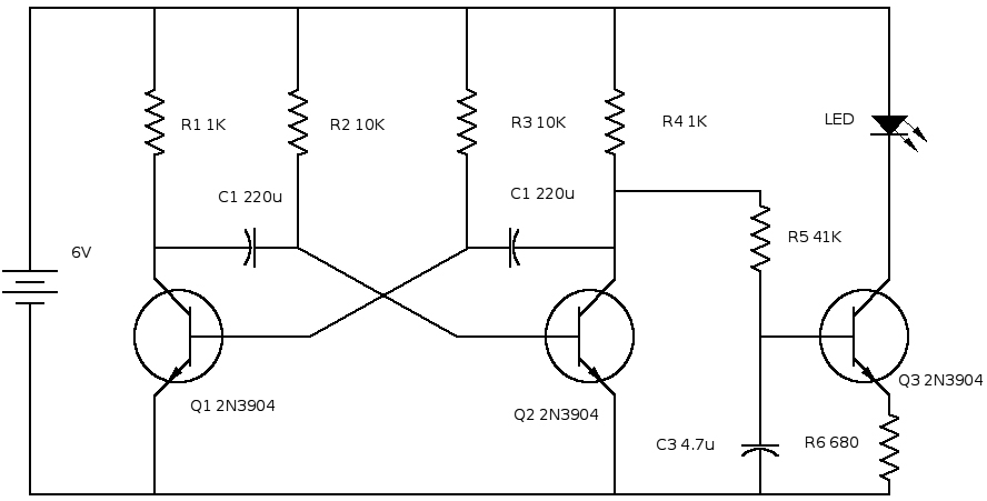
This circuit consists of two main parts. The first part is the oscillator which is a standard circuit consisting of everything on the left hand side up to and including R4 and Q2. On the right hand side Q3 and R6 form a current source that drives the LED. It is controlled by the voltage on the base of Q3. R5 controls how fast C3 charges and discharges, controlling the voltage on the base of Q3. If the oscillator is to slow, decreasing C1, C2 and/or R2, R3 will speed it up. If the fading effect is to slow, decreasing C3 will speed that up.
Christopher Rhames
via email
Ah, this is a difficult thing to do simply. First an LED is not like an old tech incandescent bulb which gets dimmer when the voltage goes down and then brighter as the voltage goes back up to its correct operating voltage.
An LED turns on at a specific voltage and turns off at a lower voltage, it will continue to give light for some voltage range as long as the current is constrained to not exceed too high a current when the LED will burn out.
So,
- An LED turns on or off depending on its driving voltage
- We can not exceed its operating current or we burn out the LED
- LEDs do not have different brightness depending on voltage.
The only way I know of making this happen is with a circuit that is called a pulse width modulator that changes the pulse width that drives the LED ON vs. OFF time. I have used an Arduino and a program sketch to do this, but I’m sure there’s someone out there who may have done this with something like a 555 timer IC which might be a “simpler” circuit. In fact I found this: Generate Pulse Width Modulation (PWM) Signal using 555 Timer IC https://circuitdigest.com/electronic-circuits/555-timer-pwmgenerator-circuit/
Notice here that the author uses a pot, variable resistor, to drive the 555 Timer IC to change it’s pulse width. This means you’ll have to hire someone to continually adjust the resistor up and down and up and down, etc, for two minute cycles to get what you want, definitely NOT realistic.
OK, so what does that resistor do? It probably changes the voltage going into the 555 timer that causes the 555 to increase or decrease the pulse width. This sounds like a sine wave of varying voltage wich could be made with another transistor circuit.
You might want to also watch: https://www.youtube.com/watch?v=QmB1Ev-h3y4 If anyone knows of a simple circuit that does this I’d like to know as well. BUT, I think the best you will be able to do is to find a Pulse Width Modulating IC to do the job and then a driving circuit to produce whatever is needed to tell the PWM IC what pulse width is needed now.This might be the IC needed, I know you said you didn’t want an IC, but even the simplest circuit used a 555 Timer IC: How to use TL494 pulse width modulation control IC 94 https://microcontrollerslab.com/tl494-pulse-width-modulationcontrol- ic/ Good-luck and I hope this helps at least a little.
Phil Karras KE3FL
Ms. Carrillo raised a question about a means of driving an LED from bright to dim, then reverse, and repeat. She further stipulated that it must be a non-IC-based circuit.
Since LED brightness is a nearly-linear function of its forward current, this suggests a triangle-waveform driver circuit. An examination of the information available on the internet for a transistor-based circuit uncovered a suitable circuit1 for which I have modified timing component values and added an output buffer, all of which is shown as Figure 1 below.
Figure 1: Schematic diagram
The circuit operates from a 12-volt source. It is comprised of two current-mirror elements Q1-Q2 and Q3-Q4, and a three-way differential comparator circuit Q5, Q6, and Q7. Current mirror Q3-Q4 functions such that the current drawn by the collector of output transistor Q4 will always be identical to the current supplied to the collector of input transistor Q3; a similar explanation can be made for the operation of current mirror Q1-Q2.
Figure 2: Charge C1
In the initial state, capacitor C1 is fully discharged. Upon application of power, R1 provides about 3.5 mA into current mirror Q3-Q4. Since the voltage at the upper end of C1 [V(C1)] is zero, Q6 is off. Q5, however, is forward-biased by the voltage divider R3-R4, thereby completing the circuit Q1-Q5-Q4, such that 3.5 mA is drawn by Q4 out of Q1. Because Q1-Q2 is also a current mirror, a current of 3.5 mA will be applied to C1 by Q2, whence V(C1) increases from zero. C1’s voltage increase is linear because the charging current is a constant value. See interval t1 in Figure 2 above.
Figure 3: Switch
Transistor Q6 turns on at the point where C1 has risen to be equal to Q5’s base voltage. In its conducting state, Q6 steals current from R3, removing base drive to Q5, turning it off, thereby turning off current mirror Q1-Q2 whence charging current is removed from C1. See interval t2 in Figure 3; “V(n004)” is the base voltage at Q5.
Figure 4: Discharge C1...
C1 discharges into current mirror Q3-Q4 via the base-emitter junction of Q6. This action provides base current to Q6, keeping it turned on until such time as the terminal voltage of C1 [V(C1)] falls below the base voltage at Q7 (set by voltage divider R1, D1 and Q3). At this point, Q7 begins to turn on, rapidly shutting off Q6. See interval t3 in Figure 4 above.
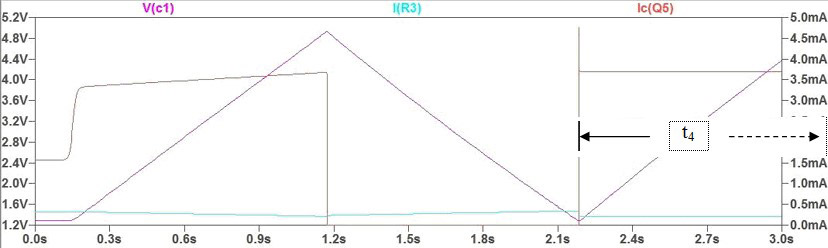
Figure 5: ... and repeat
Once Q6 is turned off, R3 can once again provide base current to Q5, turning it on; the cycle repeats. See interval t4 in Figure 5 above, being the same as interval t1 in Figure 2.
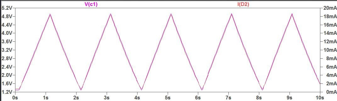
Figure 6: ... and repeat
Figures 2 through 5 show V(C1), the terminal voltage of C1, having a triangular waveform with a period of two seconds. This voltage is impressed upon the gate of MOSFET M1; diode D3 provides a DC voltage shift to better match the MOSFET’s characteristics. M1 drives LED D2 through current-limiting resistors R5 and R6, whose values have been chosen to enhance current linearity.
Figure 6 above shows the excellent match between drive voltage V(C1) and LED current I(D2). A linear drive current will produce a very nearly linear variation in light output; see Figure 7.
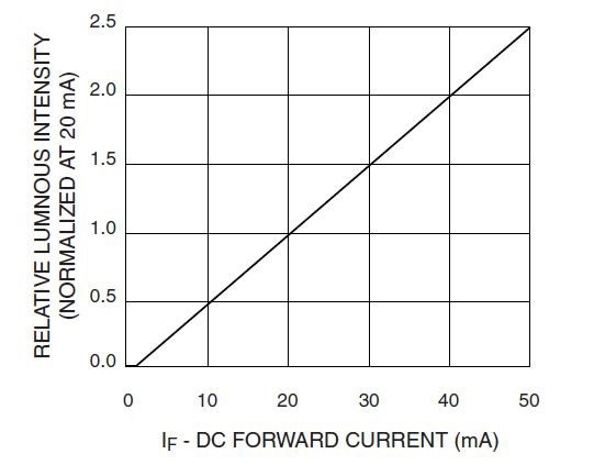
Figure 7: LED Luminosity vs Forward Current
Some words about the components used: M1 is shown as a 2N7002, which is a surface-mounted device, for which leaded part 2N7000 is a functional substitute. BS170 is another leaded version of this part. LED QTLP690C was a random choice from the LTSpice component library; choose your own with particular emphasis on current-vs-luminosity linearity. All resistors are 5% tolerance except R1, which is a 1% value. Given that the tolerance of C1 is probably not better than 10%, it would be wise to replace R1 with a 5K-ohm variable resistance to allow for adjustment if the timing is at all critical.
Current mirrors: Proper operation of a current mirror circuit requires that the silicon bodies of both transistors of the pair be at the same temperature. This is nearly impossible to achieve with discrete components, especially as in the present case when the power dissipated by the two transistors differs significantly, one from the other. Quad-transistor through-hole and surface-mount package equivalents of the 2N3904 and 2N3904 are available from Mouser and others; look for MPQ3904 and MPQ3906, respectively.
Ms. Carrillo did not specify the power of the LED to be driven. I assumed a small indicator, so that the maximum drive current provided by this circuit is just shy of 20 milliamperes. For larger, more-powerful devices, a larger MOSFET would be needed (with attendant modifications of the values of R5 and R6). A preferred approach in this case would be to use the drive current available at the drain of M1 as a means of modulating a multivibrator circuit, driving the large LED with a pulsed current whose pulse width varies according to the linear triangle-wave modulation. While such a circuit is beyond the scope of the present discussion, several, 2.3 have been found in the literature.
1 https://www.electronicspoint.com/forums/threads/7-transistors-triangle-wave-generator-650khz.264497/
2 See US Patent 3445788A, Camenzind, Pulse-Width Modulation Circuits (https://patents.google.com/patent/US3445788A/en)
3 See US Patent 3587002, Brown, Voltage-Controlled Transistor Multivibrator (https://patents.google.com/patent/US3587002)
Peter A. Goodwin
Rockport, MA
There are several simple circuits around that will do it, just google "breathing LED circuit," but there are also LEDs with the circuit built in. The only supplier I know of is Lighthouse LEDs in the US (I forget where, I buy online).
Lance Turner
East Ridgley, Australia