When a PIC can Replace a 555
Engineers Mini-Notebook 555 Circuits by Forrest M. Mimms, III ©1984. Also see www.forrestmims.org.
This third article in a recurring series continues to examine several of the circuits from the popular 555 Timer IC Circuits by Forrest Mims, which are variations on audio oscillators. Some will use the PIC replacement covered in the first article, while others will develop specific programs using a PIC which will emulate a particular implementation of a 555. The remaining oscillator circuits will be discussed in a future installment of this series.
As a quick review, the first article described a general-purpose 555 replacement by using the PIC12F1572. The second article reviewed the circuits and their PIC equivalents, which used the 555 basically as a mono-stable multivibrator.
References to the PIC replacement are to version 1.4 of the program. This version makes three enhancements to the original: all astable modes (modes 4-6) use pin 4 as a gate input; mode 5 replaces the off-time function with period; and mode 6 is a metronome.
FM-2
Circuit 2 (Schematic 1) from Mims’ book shows the 555 connected as an astable multivibrator. It shows some of the internal circuitry of the 555 which will be helpful in discussing the circuits that follow.
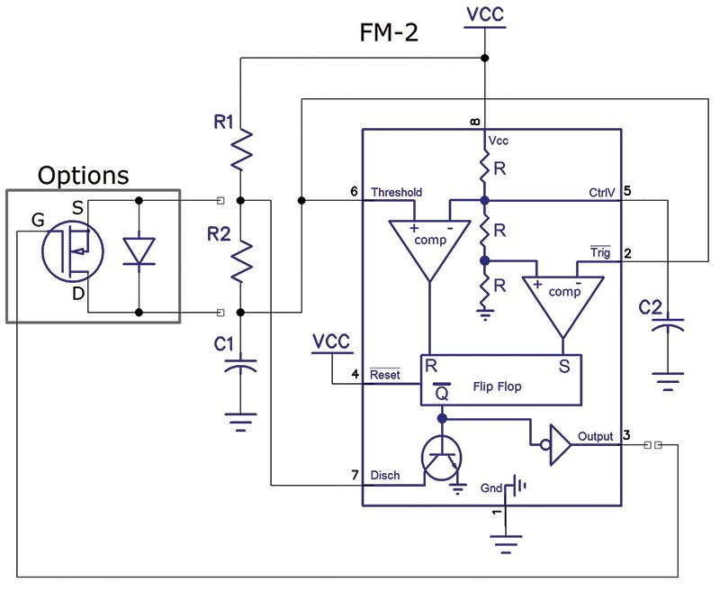
SCHEMATIC 1. Basic 555 astable circuit.
The operation of the circuit can be described briefly as:
1. Initial condition: Power off.
2. Apply power.
A. Initial C1 voltage is 0V which is below the trigger voltage (1/3 Vcc).
B. Flip-flop is set: Output high, discharge circuit off.
3. C1 charges through both R1 and R2.
4. C1 reaches the threshold voltage (2/3 Vcc).
A. Reset the flip-flop.
B. Output goes low.
C. Discharge circuit on.
5. C1 starts discharging through R2.
6. C1 voltage decreases to the trigger voltage (1/3 Vcc).
A. Set the flip-flop.
B. Output goes high.
C. Discharge circuit off.
7. Cycle starts over at step 3.
Figure 1 shows the power-up sequence of a 555 astable multivibrator.
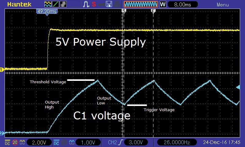
FIGURE 1. 555 astable power-up.
The output is high while C1 is charging. The first pulse is longer because the capacitor has to charge up to the threshold value (2/3 Vcc) from ground, while for the remaining pulses, C1 charges up from the trigger level voltage (1/3 Vcc).
The actual ratio of the first pulse width to the remaining pulse widths is about 1.7:1. You might initially think that the first pulse should be twice that of the remaining pulses, but the voltage rise is exponential — not linear.
All the documentation I have seen for 555 astable operation states that the charge time will always exceed the discharge time since the capacitor is being charged through R1 and R2, but is being discharged only through R2. Therefore, the duty cycle will always be greater than 50%. The higher the R2/R1 ratio, the closer to 50% you get.
If R1 = R2, the duty cycle will be 66%. If R1 gets low enough, the discharge transistor will no longer saturate, and the discharge time will be longer than the calculated value which can lead to duty cycles less than 50%.
Schematic 1 also shows two options for changing the charge time dependency on the value of R2. A diode in parallel with R2 will decrease the charge time once the voltage across R2 reaches the diode threshold value. This is about 0.6V for a typical silicon small signal diode, as low as 0.3V for a Schottky diode, and about 0.2V for germanium.ith a Vcc of 5V, the difference between the threshold voltage and the trigger voltage is about 1.66V. The diode will short R2 during a portion of the charge cycle.
If you want to make the on time totally independent of the off time, you can put an FET like the 2N7000 across R2 and drive the gate from the 555 output. The FET will short out R2 when the output is high, causing C1 to charge only through R1. Using an FET, you can easily get duty cycles much less than 50%. You will want to make sure that R1 is not so small that it could cause so much current through the FET that it is destroyed.
From a totally practical perspective, I would never have less than 100 ohms for either R1 or R2. If you are using a pot for either or both, I strongly recommend a fixed resistor of at least 100 ohms in series with each pot.
The PIC replacement circuit is shown in Schematic 2. R1 and R2 should be selected to force the 555 replacement into Mode 4 — one of its astable modes. R3 and R4 are used to select the range (see the first article for details); R5 and R6 set the off time and on time.
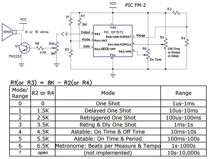
SCHEMATIC 2. PIC 555 replacement, astable circuit.
Keep in mind that for both the mode and range, it’s the ratio of the two resistors that is the determining factor.
I’ve written four sample programs (available at the article link) that demonstrate astable multivibrator operation using the PIC12F1572. Three were derived from the three samples discussed in the second article of this series.
Program 1 (ASMV-1) demonstrates the simplest and fastest astable possible, with a 50% duty cycle using programmed I/O. The pulse generation code is only two statements. The period of the square wave is six instruction cycles which — for the 32 MHz clock — will be 1.33 MHz.
Keep in mind that one instruction cycle is four clock cycles. This can be trimmed down to four instruction cycles (2 MHz) if a 25% (or 75%) duty cycle is acceptable.
Program 2 (ASMV-2) uses delay functions to create the high and low times. There are both millisecond and microsecond functions which can be called from the main loop to generate whatever duty cycle you need — within the resolution of the clock.
Program 3 (ASMV-3) is quite a bit more complex than the previous two. It uses the A/D to read a voltage which controls the period of a square wave by setting the timeout value of Timer 1.
There is no capability to have separate control over the on time and off time. The program uses an interrupt based on Timer 1 to change the state of the pulse. There are definitions in the program which allow the Timer 1 clock to be changed.
Program 4 (ASMV-4) uses the PWM module and A/D inputs to develop a variable period and duty cycle square wave.
The program was developed starting with the PIC 555 equivalent program and then modified to use the PWM module. It is well-documented, so it should be fairly simple to modify.
There are eight overlapping period ranges from about 62.4 ns (16 MHz) to 67 s (.0148 Hz). The range selection method is identical to that of the PIC 555 replacement from the first part of this series.
Schematic 3A shows the debugging connections for all my PIC programs (I’m currently using a PICkit 3), while 3B shows the application connections for ASMV-4. Due to the methods used in ASMV-3 and ASMV-4, the processor doesn’t need to be dedicated to executing the code.
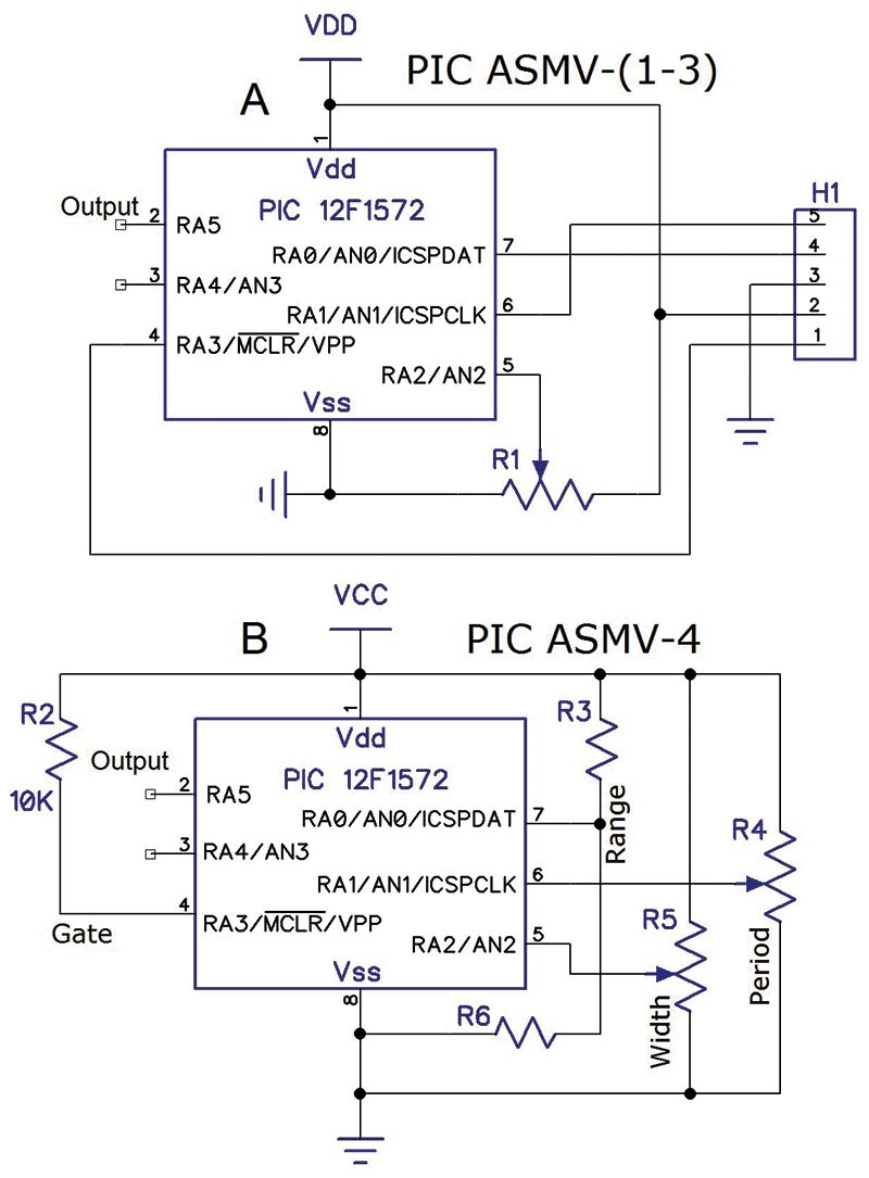
SCHEMATIC 3. PIC voltage controlled oscillator and debug connections.
FM-11
Mims’ Circuit 11 (Schematic 4) shows the 555 connected as a voltage controlled oscillator (VCO), and is basically the same circuit as FM-2.
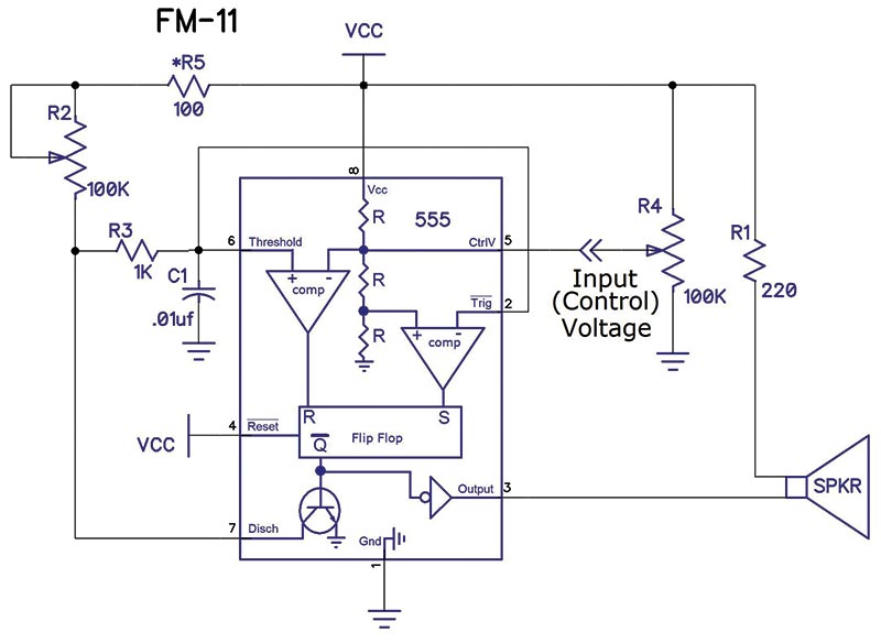
SCHEMATIC 4. 555 voltage controlled oscillator.
The major differences are the speaker and the potentiometer on the control voltage input. Normally, in most 555 applications, this pin has a bypass capacitor on it. For this application, as a VCO, it’s used as a means to vary the frequency by controlling the trip point voltages of the two comparators.
Looking at the schematic, you can see that the control voltage is one input of a comparator which has the threshold voltage as its other input. Varying the control voltage changes the frequency of oscillation because the difference between the trip voltages of the two comparators is changing. Note that the trigger voltage point will always be half of the control voltage.
As shown in the Mims book, as the control voltage decreases from 4.8V, the output frequency increases. However, an interesting characteristic of the circuit is that when the control voltage passes through some low value (about 1.6V when Vcc = 5V), the frequency decreases until the voltage gets close to 0V and the unit stops oscillating.
Take a look at Graph 1 which plots the output frequency vs. the control voltage.
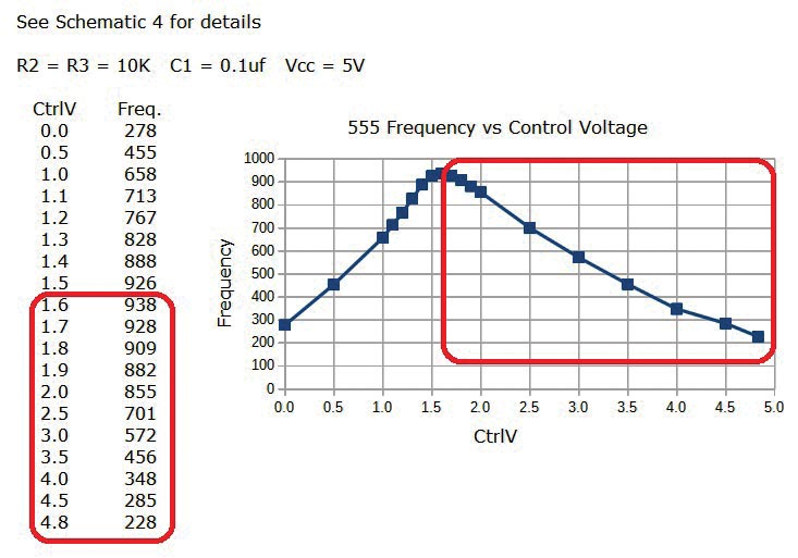
GRAPH 1. 555 VCO frequency vs. control voltage.
The spreadsheet called Graph 1.ods (available at the article link) also plots the same information for a 556, which shows the same characteristic as the 555 but with a slightly lower inflection point of 1.2V.
As part of the investigation for this article, I found that the resistors (labeled R) which form the internal voltage divider shown in the 555 schematic can be different among manufacturers. Out of nine manufacturers I found, only four listed the resistor values. Three of them were 5K and one was 100K. The 100K unit used FETs, while the others show bipolar transistors.
One way to determine the resistor values is to measure the CtrlV and then place a 47K resistor from the CtrlV to ground and measure the voltage again. If the voltage doesn’t change much, then the resistors are low value and probably 5K. All three resistors will be the same whatever their value.
The reason for the discussion above is that the book shows a 100K potentiometer on pin 5. If the voltage divider uses 5K resistors, the 100K pot will have very little effect on the voltage over approximately the center 80% of its range.
I’ve included another spreadsheet (Voltage Divider.ods) in the article downloads which shows this characteristic in a table as well as graphically.
If you want to implement this circuit, I recommend that a potentiometer of at most 5K be used; 1K would be better or — better yet — drive it from an op-amp.
Also notice the presence of R5 which is not in the book. It is inserted to ensure at least some resistance for when the pot is at minimum resistance. Having the internal discharge circuit connected directly to Vcc didn’t seem like a good idea to me. I’ve done the same thing to all of the 555 circuits in this series.
The equivalent circuit using the PIC 555 replacement (PIC FM-11) is shown in Schematic 5. By tying pins 5 and 6 together, the circuit will output a 50% duty cycle.
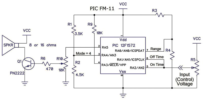
SCHEMATIC 5. PIC 555 replacement voltage controlled oscillator.
For a wide range of audio frequencies, the best range selection for the circuit is Range 1 (R3 = 6.5K, R4 = 1.5K): 10 µs to 10 ms.
This would theoretically yield a square wave frequency range of 50 kHz to 50 Hz. However, with software delays, the shortest period is closer to 60 µs, or about 16 kHz.
The higher frequencies will change more rapidly with voltage than the lower frequencies due to the 10 µs resolution/step size. For example, a 50 kHz signal has a period of 20 µs. The next longer period (lower frequency) available with this program would be 40 µs (except for the delays mentioned above), which is a frequency of 25 kHz.
The step size is 20 µs because both the on time and off time are changing simultaneously by the same amount: 10 µs per step.
I used a different circuit to drive the speaker, which should be safer for the PIC which has less current available on its outputs than a 555. The same circuit can be used for the 555 if desired.
One of the differences between the operation of the 555 and PIC circuits is the overall frequency range. The 555 is usually rated up to a maximum output frequency of 3 MHz. The PIC replacement — without any software changes — will only do up to 500 kHz.
If you want to use the PIC and need a higher frequency, the program can be modified, or you can start with program ASMV-4. However, you may need to program it specifically for your application since programming a more general-purpose device (such as the 555 replacement) will usually cause lower output frequency capability.
The 555 has a fairly linear frequency vs. control voltage characteristic as shown in Graph 1. In contrast, the PIC replacement has a very linear period vs. control voltage response. This will not work well for those applications which may want to use an analog signal to modulate the PIC for use in an FM application.
However, it’s possible to implement a numerically controlled oscillator (such as is used in DDS systems) using software in the PIC. Programs NCO-1 and NCO-2 use software timing loops to create an NCO with a 50% duty cycle. NCO-1 develops a programmable frequency of up to 400 kHz with about 6 Hz resolution. NCO-2 allows the frequency to be modified via an external potentiometer. Its range is adjustable via definitions in the program.
One feature of the PIC’s A/D that I used in one of the timing loops is that the A/D result registers are both loaded simultaneously at the end of the conversion cycle. This means they can be accessed during a conversion for any calculations that may be desired.
The output will have some amount of jitter in it due to the resolution of the timing loop. There is a timing value in one of the loops that determines the full-scale frequency. The calculations are described fully in the program comments.
Program NCO-3 uses the NCO peripheral of the PIC16F18313 to develop a square wave. Graph 2 plots the output frequency vs. control voltage of NCO-3 for Range = 0. Like the 555 replacement, it also uses a potentiometer for frequency control and a voltage divider to select from among six ranges.
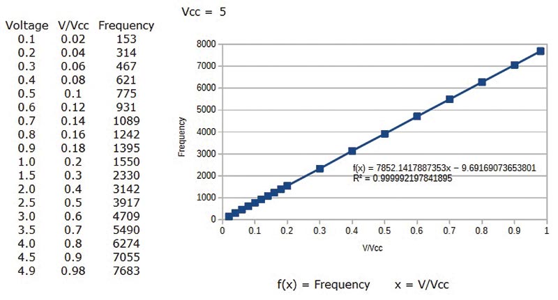
GRAPH 2. PIC NCO frequency vs. control voltage.
Range 0 is probably best for audio applications since its range is from 7.6 Hz to about 7.7 kHz in 7.6 Hz steps. RA4, pin 3, is used to enable the output when it’s low. There’s only one statement in the program which needs to be changed if high-enable is wanted.
Schematic 6 shows the connections for the NCO-3 application. Schematic 3A shows the connections for programming and debugging.
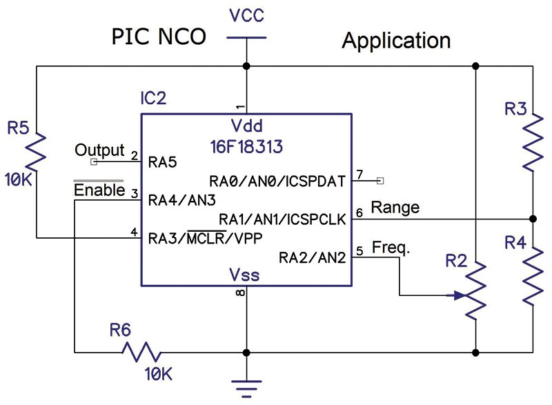
SCHEMATIC 6. PIC numerically controlled oscillator.
Once the devices are programmed for an application, pin 7 may be left floating but pin 4 should be tied high. RA3 can only be a digital input when the unit is not connected to a programmer.
FM-16
Circuit 16 (Schematic 7) is a gated oscillator which uses an FET in series with the timing resistors as the gate.
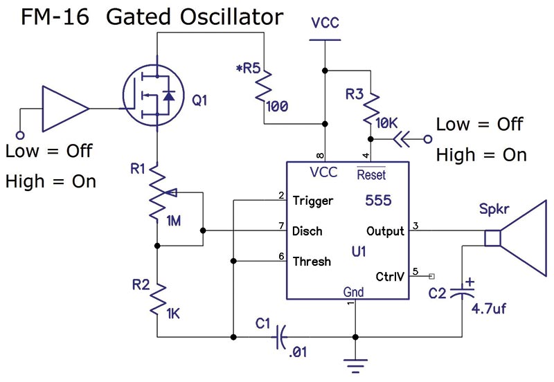
SCHEMATIC 7. 555 gated oscillator.
The FET can be replaced by directly connecting the output of the logic device to the high end of R1 if you use a device from one of the many CMOS families such as 74HC.
Either solution requires that the supply voltage be 5V or lower. If you use a device from one of the original CMOS logic families — such as the 4000 series — you can use a supply of up to 18V.
Another solution for the 555 is shown in the schematic as an option. You can simply use the Reset input to gate the oscillator. You’ll need to remove Q1 and connect R5 directly to R1.
All three astable modes of the PIC replacement for the 555 are gated. For most audio applications, mode 4 is appropriate (Schematic 5) with pins 5 and 6 tied together for a 50% duty cycle. Pin 4 is the gate input; it’s shown tied high for normal astable operation. Grounding it turns off the oscillator.
FM-20
Circuit 20 (Schematic 8) shows a 555 wired as a tone burst generator. It uses an RC network (R3, R4, C2) on the Reset input in order to enable and disable the output.
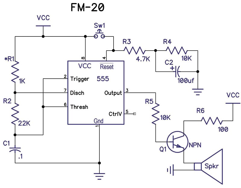
SCHEMATIC 8. 555 tone burst generator.
When the switch is closed, the output is enabled and C2 charges up to above the threshold voltage of the Reset input. When the switch is opened, C2 will discharge through R4 until it’s below the Reset threshold, which then turns off the output.
The time interval that the output remains on after the switch is opened is dependent on the R4*C2 time constant. The circuit will respond more quickly to the switch if the value of R3 is reduced; 100 ohms will work nicely.
I modified the original PIC replacement program so that it now has gated astable multivibrator modes using pin 4 as the gate input. The same circuit used by the 555 in Schematic 8 can be used on the gate input of the PIC. It will operate identically to the way in which the 555 operates, except the 555 has a 0.7V threshold whereas the PIC inputs are set up for Schmitt trigger levels with a somewhat higher threshold.
You can also use the same speaker circuit on the PIC as is used by the 555. However, I prefer the speaker circuit shown in Schematics 2 and 5.
All of the sample programs, schematics, diagrams, and pictures for this series can be found on my website (www.qsl.net/k3pto), as well as in the downloads below.
Happy PICings until next time! NV
Resources
All schematics are drawn using DipTrace
www.diptrace.com
All parts purchased are from Digi-Key
www.digikey.com
My website
www.qsl.net/k3pto
Downloads
What’s in the zip?
Source Code
Graphs