World’s Smallest Transistor — Sort of
By Jeff Eckert
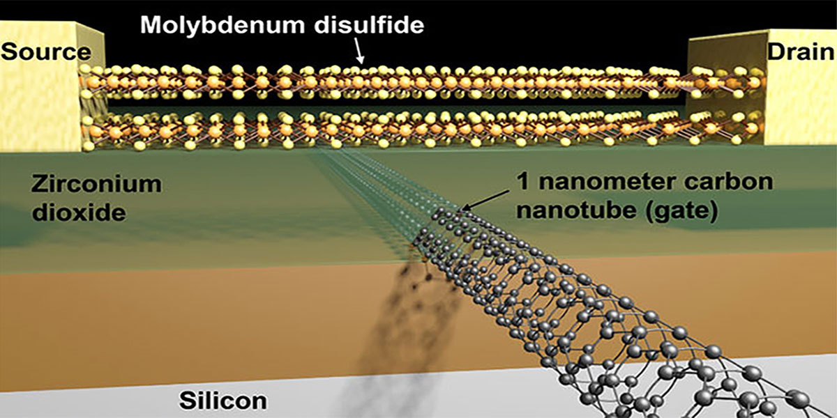
According to the laws of physics, an operational transistor gate can be no smaller than 5 nm, which is about a fourth the size of today’s commercially available 20 nm gate transistors. This is because below 5 nm, a phenomenon called “tunneling” takes place in which the gate barrier can no longer keep the electrons from zipping straight from the source to the drain terminals, and the transistors can’t be turned off. However, lawbreakers at Berkeley Lab (www.lbl.gov) observed that this is true when we’re talking about silicon, but not necessarily other semiconductor materials. By using molybdenum disulfide (MoS2) as the semiconductor material, they managed to create a gate only 1 nm in length. (One nice thing is that MoS2 is not a particularly exotic or expensive material and, in fact, is sold in auto parts stores as a lubricant.)
Part of the explanation as to why the device works is that “electrons flowing through MoS2 are heavier,” so their flow can be controlled with smaller gate lengths. This is something of a head-scratcher, given that yours truly has always been led to believe that all electrons have exactly the same mass. (In fact, Prof. John Wheeler — no slouch in the physics field — went so far as to claim that all electrons are the same because, in fact, there is only one in the entire universe, and we are just looking at it on different slices of space time. But let’s not go there.)
Another factor is that MoS2 can be produced in thinner sheets (≈ 0.65 nm) which also helps to control the current flow.
As with most early developments, it’s a long way from commercial implementation. As observed by Berkeley scientist, Ali Javey, “We have not yet packed these transistors onto a chip, and we haven’t done this billions of times over. We also have not developed self-aligned fabrication schemes for reducing parasitic resistances in the device. But this work is important to show that we are no longer limited to a 5 nm gate for our transistors.”▲
Comments