The creation of the integrated circuit (IC) stands as one of the most important inventions of mankind. Today, nearly all modern products use this chip technology.
These ubiquitous microchips led directly to groundbreaking advances in computing, communications, medicine, and practically every technically related field. Without them, developments such as the personal computer, cell phones, the GPS system, and the Internet would not exist.
Microchip development started in the decade after the invention of the transistor at Bell Labs in 1948. Thus, while transistors were remaking radios, television sets, computers, and other products from the tube era, another technology even more revolutionary was taking shape. It had become apparent that transistorized products would not expand the electronics market unless they were greatly miniaturized.
Clearly, there wasn’t much progress to be made by hand soldering separate components into circuits. For this reason, a number of people began thinking about better ways of miniaturizing circuits. This work eventually culminated in a huge integrated circuit industry generating hundreds of billions of dollars a year in sales worldwide. That’s several million square meters of silicon wafers!
In this article, we’ll look back on this period that launched the serious development of integrated circuits. This story is one of individual genius, forgotten contributors, amazing new technology, and brutal patent fights. We’ll examine the contributions of the personalities and organizations involved, as well as the impetus that led to this landmark technology.
Introduction
At the Institute of Radio Engineers’ (IRE) annual trade show in New York on March 6, 1959 Texas Instruments proudly introduced a new device that would change the world as profoundly as any invention of the 20th century: the integrated circuit. Unfortunately, hardly anyone noticed!
This is understandable since it was an era of marvelous advances: jet planes, rockets, computers, and medical breakthroughs. Besides, who could tell if some little gizmo — one of many being developed — would be transformative or just fizzle? Even the New York Times only took two paragraphs out of their main story to mention it. The main story was about Westinghouse’s new radar system that would let motorists drive the highways with their hands off the steering wheel.
They proposed lining the nation’s highways with foil strips coded in dots and dashes. Radars on the car’s bumper would control the steering wheel to keep the car on course. This seemed more futuristic and appealing than a tiny device that didn’t have a clear role in the future of electronics.
Work on this tiny device had begun early in October and was to consist of a germanium based flip-flop. Although it wasn’t the first IC ever built, it was the first IC to be built from scratch using two diffused base transistors, two capacitors, and eight resistors. The unit was less than 1/4 inch long, 1/8 inch wide, and 1/32 inch thick — quite small compared to the equivalent printed circuit device.
Although very small, it performed as well as circuits that were many tens of times bigger. The first working units were completed in early 1959 and later used for the first public announcement of the “Solid Circuit” (integrated circuit) concept at the IRE show (Figure 1).
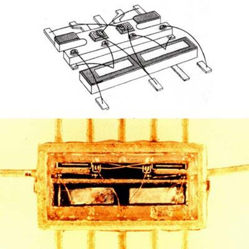
Figure 1. The Type 502 Bistable Multivibrator Solid Circuit (1960). It’s based on the concept announced at the IRE show in March 1959.
Even though the public could not see the importance of this advancement, TI’s President Patrick Haggerty understood its significance. He predicted the circuits first would be applied to the further miniaturization of electronic computers, missiles, and space vehicles, and said that any application to consumer goods such as radio and television receivers would be several years away.
So, with this inauspicious beginning, the integrated circuit was introduced to the world. At the time, who could know that this was the debut of a technology that would usher in a wide array of circuits with integrated functions — logic gates, shift registers, flip-flops, amplifiers, microprocessors, and countless others that would be built by many companies amid furious industrial competition.
There seems to be no consensus on who invented the IC. In the 1960s, four people were thought to be responsible for it: Jack Kilby, Kurt Lehovec, Robert Noyce, and Jean Hoerni. In the ’70s, this list was shortened to Kilby and Noyce and then to Kilby. However, in the 2000s, historians and others reinstated the idea of multiple IC inventors.
In what follows, we’ll have more to say about the inventors and how they accomplished their goals. It’s a captivating story about the invention of integrated circuits and the people and companies involved in this pursuit. To get started, let’s look at what prompted this epic quest.
The Road to Reliable Circuits and Miniaturization
Early electronic equipment was composed of only a few dozen components and could be easily assembled by hand soldering methods. For reliability, each part (resistor, tube, capacitor, etc.) was manufactured separately using a process optimized for the component. As the equipment became more complex, shortcomings in this procedure began to appear. Circuit costs started to increase more rapidly than the component count, with circuit reliability suffering a corresponding decrease.
Because of their inherent complexity, military systems were the most vulnerable to this phenomenon, often called the “the tyranny of numbers.” It was observed that some electronics equipment reached a level of complexity such that losses from failures and downtime exceeded the expected benefits.
This was first noticed during World War II when each Boeing B-29 (one of the most complex systems of the time) carried many hundreds of vacuum tubes and thousands of passive components. Similarly, in 1946, the ENIAC computer used more than 17,000 vacuum tubes and many thousands of other parts; each component reducing the reliability and increasing repair time.
These designs were limited by the ubiquitous vacuum tube which was large and expensive in comparison to most passive components. Their life was limited, making frequent replacements necessary. They also dissipated large amounts of power, requiring extensive cooling. It seemed that using traditional electronics was reaching a deadlock and it was necessary to look at further development aimed at reducing the number of components. However, these factors changed dramatically in 1948 with the invention of the transistor. Figure 2 illustrates the progression from tubes to transistors.
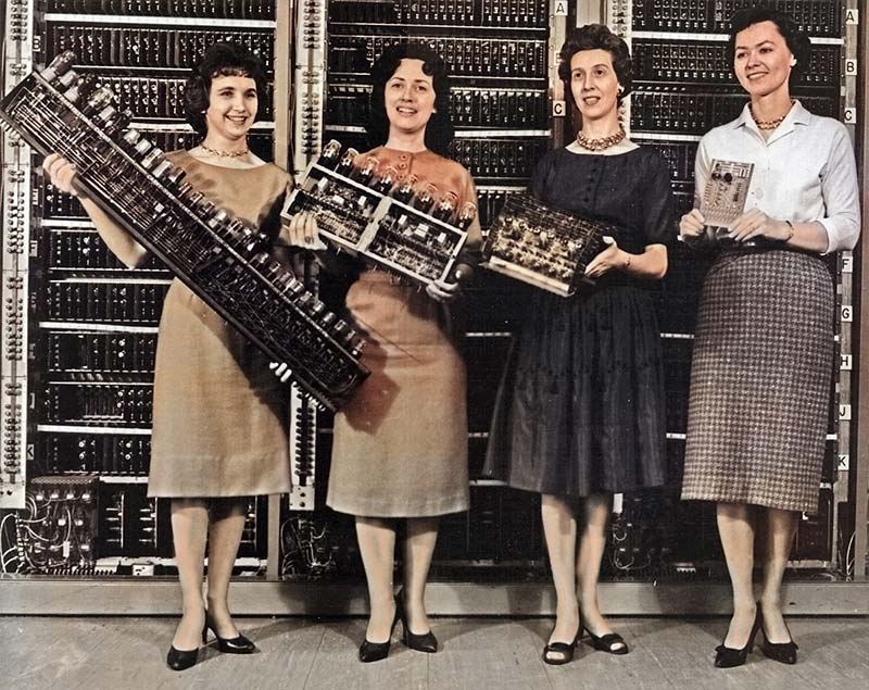
Figure 2. In 1962, four women programmers hold parts of the first four Army computers. From left is the ENIAC board, EDVAC board, ORDVAC board, and the BRLESC-I board. Image courtesy of the US Army.
Transistors led to the expectation of a new technological revolution. Scientists and fiction writers proclaimed the imminent appearance of spectacular computers, intelligent machines, and robots to aid us in all aspects of our life. While transistors had the potential to reduce size and power consumption, they could not solve the problem of reliability of complex electronic devices. In fact, dense packing of parts in some transistorized products often hindered their repair.
As components in these ever more complex systems increased into the thousands, the number of interconnections was exploding. Each transistor had three leads that needed to be attached as well as all the diodes, resistors, capacitors, and other elements that needed to be connected. This tedious task of soldering was done by hand, usually by assembly lines of women who possessed greater dexterity than men. Given thousands of solder joints in a circuit, chances were high that a few of them would be faulty ruining its operation.
So, while the transistor solved some problems, its success allowed another problem to emerge. Thus, in the 1950s, it seemed that reliability was at its theoretical limit with no improvement in the interconnections between components in sight.
First Ideas for Integration
Early attempts to integrate circuits go back to 1949 when a German engineer, Werner Jacobi conceived of a semiconductor amplifier having five transistors on a common substrate in a three-stage amplifier circuit. In his patent, Jacobi disclosed small hearing aids as a typical application of his device. However, no commercial use of this invention was ever reported.
In the 1950s, designers were obsessed with the problem of reliability combined with the bigger concern of miniaturization. Military designers needed to cram their electronics into the smallest, lightest packages possible. Navy funding for project Tinkertoy was followed by the Army Signal Corps Micr-module program. These programs sought to make connections in a uniform, reliable, mass-produced fashion akin to the printed circuit boards that were becoming commonplace. This led some engineers to begin looking for ways to fashion electronic circuits from a single block of material.
An expert in electronic reliability, Geoffrey Dummer (Figure 3) with Britain’s Royal Radar Establishment (RRE) was also considering this problem.
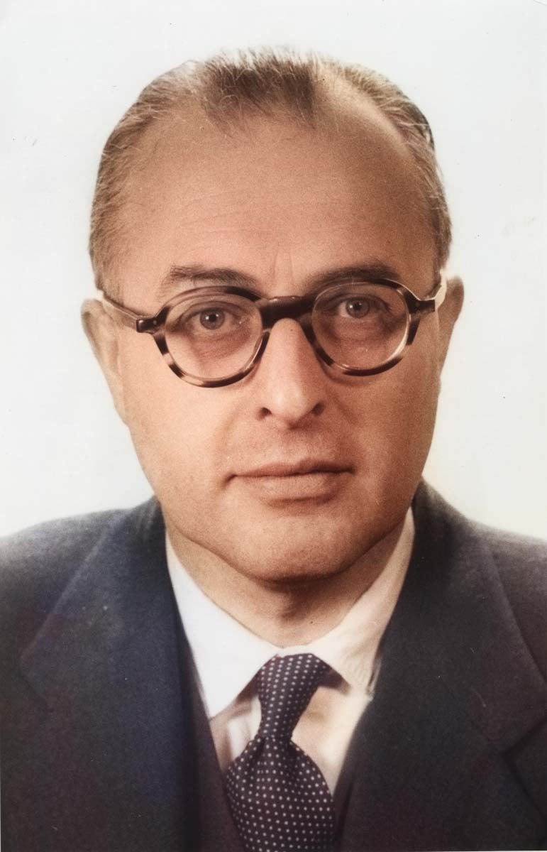
Figure 3. Geoffrey Dummer was an English electronics engineer and consultant who, in 1952, is credited as being the first person to conceive of an integrated circuit. He later worked with Plessey Research Labs in 1957 to demonstrate how a circuit might be fabricated from silicon.
It seemed to him that miniaturization and reliability were intertwined; the fewer the parts and interconnections, the higher the reliability. To him, this was the key to the problem.
In an invited paper presented at a components reliability symposium in Washington, D.C. on May 7, 1952, Dummer presented his ideas for integrating circuits. He predicted that “with the advent of the transistor, it now seems to be possible to envisage electronic equipment in a solid block with no connecting wires. The block may consist of layers of insulating, conducting, rectifying, and amplifying materials, the electrical functions being connected by cutting out areas of the various layers.”
Considering modern IC technology, his vision was amazingly close to the mark. Unfortunately, the technical problems were huge and no one knew how to solve them.
It’s hard to know the exact effect of Dummer’s prediction on subsequent research in the US, but his idea was not forgotten in Britain. In April 1957, the RRE placed a contract with Plessey Research Labs to develop a “semiconductor integrated circuit.” On September 1957 at another symposium — this time in England — Dummer and Plessey displayed a fabricated model to demonstrate how a “flip-flop” might be fashioned from silicon crystals. It received some attention from visiting Americans, but the RRE was unconvinced of its potential and the contract was not renewed.
Dummer’s self-proclaimed “peep into the future” was realized only one year after the symposium when the first crude integrated circuit was actually built — but it wasn’t in England! The event occurred in the United States at Texas Instruments where inventor Jack Kilby (Figure 4) was blissfully working, unaware of Dummer’s prediction.
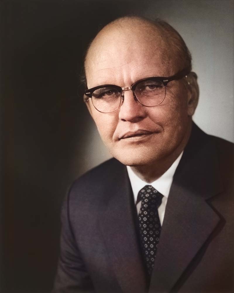
Figure 4. Jack Sinclair Kilby was an American electrical engineer credited with inventing the integrated circuit in 1959. For this achievement, he was awarded the Nobel Prize in Physics on December 10, 2000. Kilby is also the co-inventor of the handheld calculator and the thermal printer, as well as seven other inventions.
Kilby Enters the Picture
A husky, raw boned Kansas boy who stood six foot six, Kilby grew up with grease on his pants and electricity in his veins. Born in 1923, he spent most of his boyhood in Great Bend, KS, smack in the middle of the dust bowl in the Great Depression. He grew up not as a farm boy but as the son of the president of a power company that had survived the infamous Insull trust. His father was an electrical engineer, and they frequently rode together in the family Buick on visits to the utility’s widely separated plants — often getting dirty diagnosing problems with the big generators and transformers.
When Roosevelt’s new Federal Communications Commission (FCC) began issuing ham licenses, Jack studied hard, passed the test, and was granted the call letters W9GTY for his own radio station. Later on, missing the MIT entrance exam by a few points in 1941, he headed for the University of Illinois.
His studies were interrupted by Pearl Harbor and a stint with the OSS in Burma and China working on radio communications for guerrilla units operating behind Japanese lines. After the war, he finished his degree and in the fall of 1947, headed to Milwaukee for his first job at Centralab.
Kilby, now 30, started at Centralab as a junior engineer working on silkscreening techniques for depositing resistors and conductors. This procedure was pioneered by Centralab during the war, and they were now extending it to hearing aids and radio parts. In 1952, Kilby and his boss, Robert Wolff attended the Bell Labs transistor course and obtained a license for the technology. Back at Centralab, they set up a small facility to make transistors for hearing aids. Wolff recalls that “a lot of Jack’s ideas went into those transistors, and he was responsible for our first really small transistorized hearing aid.”
After attending a transistor symposium at Bell in January 1956, Kilby learned about the new diffusion technologies and how to use them for germanium and silicon. He saw, like many others working at the frontiers of electronics, that the future of transistors was in silicon. Retooling Centralab’s lines for silicon would require a half million dollars — something that the small company did not have. Kilby said later “that he felt changes in this field were coming so rapidly that it would be impossible for very small groups with limited funding to be competitive.” So, he decided to leave.
In early 1958, Kilby wrote to about a dozen leading electronics companies describing his work and ideas for miniaturization. After several interviews, he decided on the company that pioneered the silicon transistor.
Kilby’s Integrated Circuit
When Kilby arrived at Texas Instruments, they were looking for ways to become involved in the Army’s Micromodule program. This approach used components and printed circuits on tiny wafers of the same size and shape which were then tied together like a stack of rectangular poker chips.
Kilby was hired by Willis Adcock who was starting a small research group on semiconductors and said that Kilby “fit right into our plans.” When Kilby joined the group in May 1958, he recalled his duties were not precisely defined — “just something in the general area of miniaturization.”
Since radio was a big part of the electronics business, he proposed making an IF strip in tubular form that would be preferable to the wafers in the Micromodule. After spending a few months on this project, building a couple of models, and looking at the costs, it seemed like a losing proposition. This task was completed just a few days before the plant shut down for a mass vacation.
As a new employee, Kilby had no vacation time coming and was left alone in a deserted plant to ponder the lessons of the IF strip. According to Kilby, “It became clear that there were some things semiconductor houses could do very well and that they had some potent techniques that this IF strip did not make very good use of.” Then, there was a surge of inspiration.
He wrote in his notebook, “Extreme miniaturization of many electrical circuits could be achieved by making resistors, capacitors, transistors, and diodes on a single slice of silicon.” Continuing on for five pages, he showed how to realize these components in practice as well as how an entire circuit could be assembled on a single silicon wafer.
These writings in Kilby’s notebook describe a double diffusion process by which a bi-stable multivibrator (flip-flop) could be fabricated with “conductive material evaporated to connect the transistor emitter and base to the circuit, or small wires might be attached by thermal bonding.”
When everybody returned from vacation, Kilby had ironed out his ideas and presented them to Adcock, who suggested first making the flip-flop from discrete silicon parts connected in the usual manner with wires and solder. Kilby quickly built up the circuit using grown junction transistors and resistors formed by cutting small bars and etching to value. Capacitors were cut from silicon power transistor wafers, metalized on both sides. It was assembled and demonstrated to Adcock on August 28, 1958.
Although this test showed that circuits could be built with all semiconductor elements, it was not integrated! So, Kilby set out to build an oscillator circuit on a single piece of silicon (Figure 5).
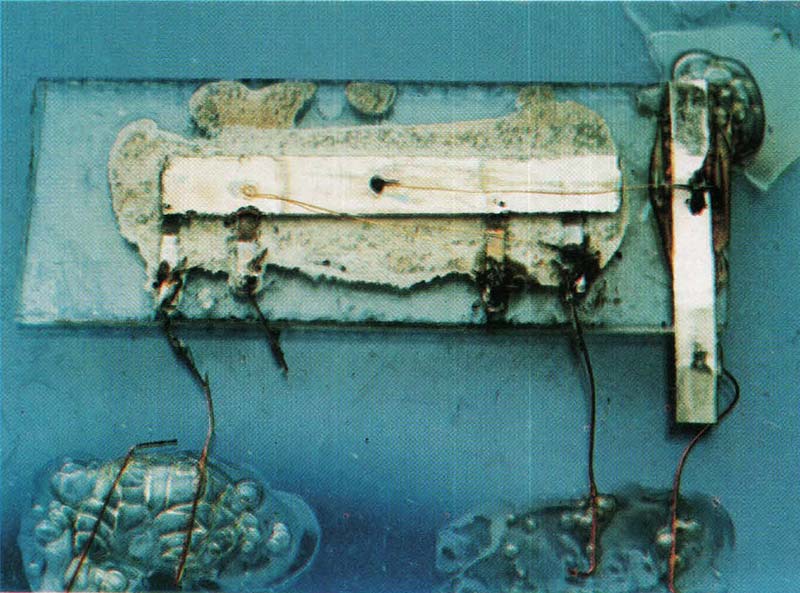
Figure 5. Shown here is Kilby’s first IC, a phase shift oscillator. It’s made out of germanium (large rectangle) and contains a single junction transistor (under the aluminum bar in the center). The short perpendicular tabs are input and output terminals. The large vertical bar on the right is ground. Wires are made of gold and the entire device is held together with wax. It’s 0.062 inches long and 0.04 inches wide.
Because of production problems, no silicon wafers were available to him. However, he did get hold of some germanium wafers in which the transistors had been diffused and the contacts evaporated.
From these, he made a phase shift oscillator by having a young woman apply wax by hand to mask mesas for the transistor and the distributed RC network. Kilby said it was done this way to provide the quickest demonstration he could get. “It looked crude and it was crude,” Kilby confessed — but it worked!
On September 12, with Adcock and some others looking on, Kilby applied 10 volts to the circuit and it sprang into action. A wavy line on the oscilloscope indicated that it was oscillating close to 1 MHz. Thus, the era of monolithic electronics was born!
Later that month, he demonstrated a two-transistor flip-flop using the same crude method, again made of germanium. Soon afterward with the arrival of photolithography expert Jay W. Lathrop, photomasks and other parts were fabricated. By the end of December, Kilby had built diffused layer resistors and capacitors using oxide layers on silicon and he had indicated how these parts might be evaporated on top of an oxide layer. On February 6, 1959, Kilby applied for a patent on “Miniaturized Electronic Circuits,” which was issued on June 23, 1964. His patent shows the phase shift oscillator and multivibrator with thermally bonded wires.
However, the patent text says that “electrically conducting material such as gold may be laid down on the insulating material to make the necessary electrical connections.”
Although the military was informed of this progress, they were not enthusiastic. Nevertheless, they awarded TI a contract for further investigation in the spring. In March at the IRE show, TI went public calling it the most significant development since the silicon transistor.
Noyce and Fairchild
In 1959, rumors of TI’s looming IRE show announcement had spread to the little Fairchild Semiconductor Co. in Mountain View, CA and it spurred activity. Fairchild had been formed only two years earlier as a spin-off by eight young scientists who had left William Shockley’s transistor company, started in Palo Alto in 1955.
Fairchild was headed by 31 year old Robert Noyce (Figure 6).

Figure 6. Robert Noyce was an American physicist who co-founded Fairchild Semiconductor in 1957 and Intel Corporation in 1968. He is credited with co-inventing the first integrated circuit along with Jack Kilby in 1959. His realization of the microchip fueled the computer revolution and gave Silicon Valley its name.
He was yet another product of the Midwest, growing up in several small Iowa towns where his father was a congressional preacher. Noyce recalls that “like so many boys of that time and place, he got exposed to a lot of mechanical gadgets, and one of the things you did was tear the Model T apart and put it back together.” Two of his three brothers also went on to technical careers.
Noyce attended school in the small agricultural town of Grinnell just east of Des Moines. He took physics courses in high school “because I mowed the lawn of the local physics professor, who was a very sympathetic character.” That professor was Grant Gale, who was a classmate of John Bardeen, one of the discoverers of the point contact transistor. Gale obtained one of their first transistors which influenced Noyce greatly, who was by then a junior in Gale’s physics class at Grinnell College.
Graduating from Grinnell in 1949, he went on to MIT for a PhD in physical electronics and then in 1953 joined Philco which was starting a big program on transistors. Three years later, he joined Shockley Semiconductor, staying only 18 months until frustrations caused him to join seven of his associates in forming Fairchild.
Fairchild had started out to make high speed, double diffused mesa silicon transistors. The mesa technique involves etching a tiny plateau — called a mesa — on the silicon wafer. After diffusing a layer or two of dopants into this surface, workers applied an inert patch (such as wax) to it and treated the surface with acid, dissolving the semiconductor away everywhere except under the patch. Fine wires were then attached to the layers forming a mesa transistor. Just about everyone in the business — Fairchild, Motorola, Texas Instruments, and others — used this approach to make diffused base transistors.
The mesa process had problems. Dust and other impurities could easily foul the P-N junction in the mesa, spoiling the transistor. This was a serious flaw that plagued engineers. However, one of the founders of Fairchild made a major discovery which propelled it to the top of the transistor industry.
Seeking a solution to these reliability issues, the Swiss born Jean Hoerni in 1958 (Figure 7) conceived the idea of a new planar manufacturing process.

Figure 7. Jean Hoerni was a Swiss-American engineer who pioneered the silicon transistor. He was one of the eight founders of Fairchild. He is credited with developing the planar process — an important technology for integrated circuits.
He suggested that instead of etching away silicon to form the exposed P-N junctions, why not embed them in the protective coating of silicon dioxide. Noyce observed that, “When this was accomplished, we had a silicon surface covered with one of the best insulators known to man. So, you could etch holes through to make contact with the underlying silicon.” This allowed impurities such as gallium to diffuse right through the layer.
Planar devices proved to have better electrical characteristics — specifically, far lower leakage currents — which is critical in logic design. And, as was seen later, they permitted fabrication of all the components of an integrated circuit from one side of a wafer.
About this time, Noyce began thinking about the same problem as Dummer and Kilby had pondered — how to make a monolithic circuit. On January 23, 1959, he said, “All the bits and pieces came together.” He outlined in his notebook a method for making “multiple devices on a single piece of silicon in order to make interconnections between devices as part of the manufacturing process …” His notes mentioned how devices could be isolated from one another with P-N junctions, how resistors would be included, and how connections could be made by evaporating metal through the holes in the oxide to interconnect the diodes for a particular circuit.
In his later interviews, Noyce stressed that it was simply a matter of using techniques that already existed. He was motivated by the fact that diffusion technology allowed the making of hundreds of transistors on a slice of silicon. He noted that, “then people cut these beautifully arranged things into little pieces and had girls hunt for them with tweezers in order to put leads on and wire them all back together again; then we would sell them to our customers, who would plug all these separate packages into a single printed circuit board.”
At this time, the Air Force was placing its hopes on molecular engineering concepts — building up a structure atom by atom that would provide a useable electronic function. Noyce believed that the molecular concept was wrong for the time “because the real strength of the electronics industry has been to synthesize something out of very simple elements rather than trying to invent a complex element. The real key to progress was to see if you couldn’t devise the various elements you would need to build a circuit and then put these together.” This idea coincided with industry chitchat to the effect that it would be nice to be able to make the whole thing in one piece instead of having to fabricate it out of a lot of different pieces.
Hoerni’s Planar Transistor Is the Key
Noyce said that for him the real key to the integrated circuit, after batch processing, was Hoerni’s planar transistor (Figure 8).
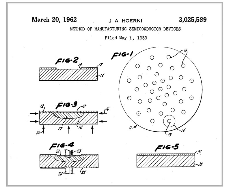
Figure 8. Jean Hoerni’s planar process as described in his patent. This process is used to build individual components of a transistor and connect them together.
“When this was accomplished, we had a silicon surface covered with one of the best insulators known to man, so you could etch holes through to make contact with the underlying silicon. Obviously, then, you had a whole bunch of transistors embedded in an insulating surface, and the next thing was that instead of cutting them apart physically, you cut them apart electrically, add the other components you needed for circuits, and finally the interconnection wiring.”
Noyce noted that there were several techniques involved but “the main one was, basically, to build back-to-back diodes into the silicon between any two transistors so that no current could flow between the two in either direction.” A resistor was the other element needed. It consisted of a diode-isolated piece of silicon that acts as a resistor. You now had resistors and transistors, and could start building logic circuits, which you could interconnect by evaporating metal on top of the insulating layer. Thus, it was a progressive buildup of the bits and pieces of the technology to make the entire thing possible.
On January 23, 1959, Noyce noted, “It was a question of having these rather vague concepts of insulators, of isolation, of interconnection, and the photoengraving for the patterns, so that you drew on your bag of tricks to combine these elements to make the integrated circuit. There was no huge light bulb flashing, but it was almost as if you sat down as a semiconductor physicist and asked, ‘How can I do this job?’ There is no doubt in my mind that if the invention hadn’t arisen at Fairchild, it would have arisen elsewhere in the very near future. It was an idea whose time had come, where the technology had developed to the point where it was viable.”
Junction Isolation Invented by Lehovec
Unknown to Noyce, far away in North Adams, MA, the research director of Sprague Electric Co., Kurt Lehovec (Figure 9) was looking for better ways to make alloy junction transistors.
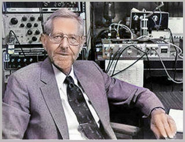
Figure 9. Kurt Lehovec was one of the pioneers of the integrated circuit. He patented the concept of P-N junction isolation used in every circuit element with a guard ring -- a reverse-biased P-N junction surrounding the planar periphery of that element. He also pioneered LEDs and lithium batteries.
Lehovec, a Czech-born physicist, was working on a technique of alloying from a liquid column to a semiconductor wafer, called capillary alloying.
Lehovec, who later became a professor in the Materials Science and Electrical Engineering Department at the University of Southern California, says once he had developed capillary alloying, he then began thinking about how to put several transistors on one wafer in order to get smaller size and save separate encapsulation.
He recalled that, “Everyone knows a P-N junction biased in the reverse direction blocks current, so it didn’t take a great deal of development to show this would work.” He immediately realized the importance of his discovery. In order to save time, he proceeded to write up the patent application and file it himself, bypassing the slower company patent attorney. It was filed on April 22, 1959, and the “Multiple Semiconductor Assembly” patent was issued on April 10, 1962, and assigned to Sprague. Because Lehovec was under salary with Sprague, he was paid only one dollar for this invention.
Development of the Integrated Circuit at Fairchild
Historians are not clear as to the events leading up to the IC at Fairchild. At the time, Fairchild was comprised of the eight founders of a closely aligned group who had worked at Shockley. They knew each other very well and often just bounced ideas around with each other. Neither Noyce nor his associates were able to recall how Noyce’s idea was accepted as a mainstream corporate project. One of the founders, Victor Grinich, said it was “one of those things that just happened — one of those obvious things.” He was surprised to learn Noyce had patented it — but called it “a stroke of genius.”
Another founder, Gordon Moore, recalls when Fairchild heard about the impending TI announcement, Noyce called a meeting to explore how they should apply Fairchild’s know-how to the problem of putting several components together on a silicon chip. It was during that meeting that Noyce first discussed with his associates his ideas about using junction isolation to separate the components and of depositing an adherent metal film over the silicon oxide as in the planar transistor.
Moore says that the project began a few months later. Moore, who was then head of engineering, remembers there were difficulties with lead bonding and with achieving the junction isolation. Nevertheless, in February 1960, Fairchild announced that it was life testing “large numbers” of what it called its micrologic elements. Noyce’s patent for a “Semiconductor Device-and-Lead Structure” was filed July 30, 1959.
Near the end of 1961, both Fairchild and TI were turning out commercial integrated circuits in production quantities. Several other companies were also considering entering the fray. Integrated circuits had arrived — made practical by the advent of planar technology with leads on top of the oxide!
Kilby vs. Noyce
The stage was now set for a battle over the patent rights to the integrated circuit. Both Kilby and Noyce had patents for the integrated circuit that looked very similar. Kilby filed his application in February 1959 and Noyce filed in July of the same year. Immediately after Noyce’s patent was granted in 1962, TI declared interference against the Noyce patent. Realizing the stakes involved, a fierce battle ensued. The lawsuit, Kilby vs. Noyce, was widely known, and it took about 10 years for them to reach the verdict. Let’s take a closer look at the issue involved.
Figure 10 shows the integrated phase shift oscillator circuit invented by Jack Kilby, whose patent application was filed in February 1959.
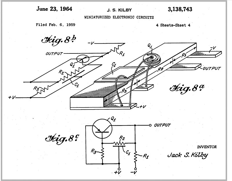
Figure 10. Kilby’s integrated circuit patent showing the phase shift oscillator. Methods for making flip-flops and other devices were also in the patent
It was configured with a mesa transistor, bulk resistor, and diffusion capacitor, connected with gold wire bondings.
Figure 11 shows the Planar IC invented by Robert Noyce.
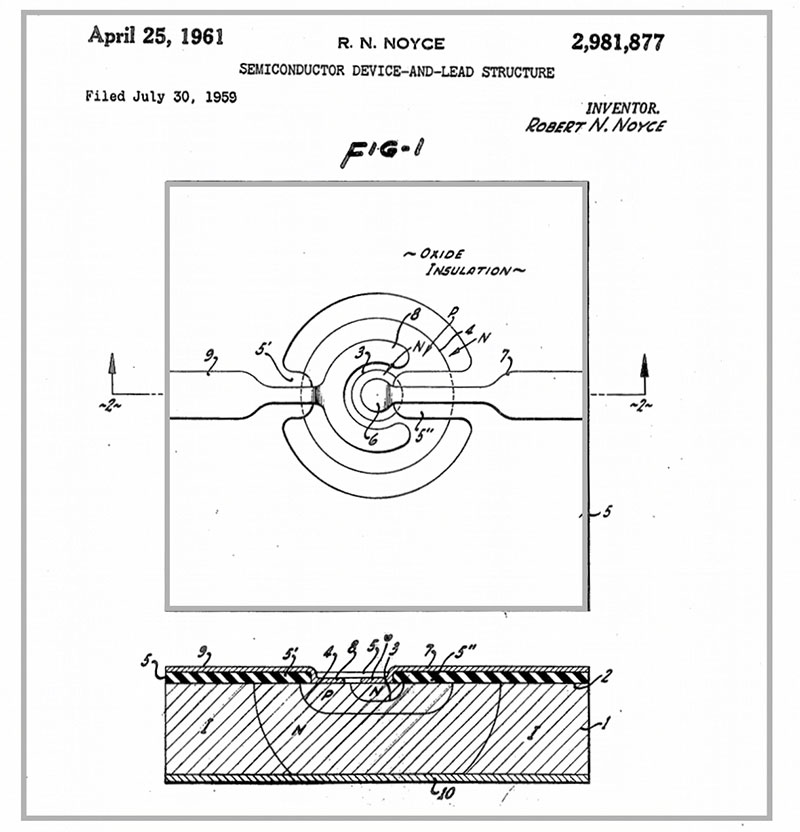
Figure 11. Noyce’s planar integrated circuit patent showing the transistor and lead structure. A C-shaped ring forms the base contact.
It was composed of an oxidized film which acted as an insulator, and interconnects formed by vapor-deposited metal.
The main point of the dispute was the method of interconnecting the components. Kilby’s patent taught that: “For the electrical contacts, instead of using the gold wire, other methods are also possible. For example … to vapor-deposit the silicon oxide film onto the semiconductor circuit wafer … Next, laying down the gold or other material on top of the “oxide” to form the necessary electrical connection.” This is basically a form of the first IC that Kilby created.
Noyce’s patent taught: “Depending on past methods, electrical contacts … the wire must be directly connected to the ‘components.’ … By this invention, the lead wires can be adhered at the same time and with the same method as the components themselves.” This is close to current IC technology.
The court conclusion came down to the terminology of “laid down” and “adhered” used in each of the patents. In 1969, the appellate patent court made the final verdict that “Kilby’s didn’t prove the term ‘laid down’ always meant or later came to mean the same as “adhere” in either electronic or semiconductor technologies.” This was in favor of Noyce, but the Kilby side complained and requested the Supreme Court for reconsideration, only to be rejected.
Happily, the rights of both companies came to be owned and cross-licensed by both parties. This was due to the fact that both companies had previously agreed to settle the trial in this way in the summer of 1966 before the final verdict!
Epilog
Despite having been championed in England as early as 1952, Kilby, Noyce, and others have suggested that the integrated circuit could only have been invented in the US. Clearly, a broad base of semiconductor technology did not exist in England at the time of Dummer’s 1952 prediction but did exist in the US in 1958. Kilby felt that Dummer was probably headed toward a dead end in actually implementing his concept, because “he started too soon when the only technology was grown junction stuff.”
Historians agree that although the integrated circuits that were developed at TI and Fairchild were not the molecular electronics the Air Force was advocating, the military was important in establishing the motivation to miniaturize as well as in ultimately becoming the first customer. It’s clear that the integrated circuit was no accidental invention like penicillin or the Gunn-diode effect.
Kilby and Noyce both received the National Medal of Science and today are celebrated as co-inventors of the integrated circuit (Figure 12).
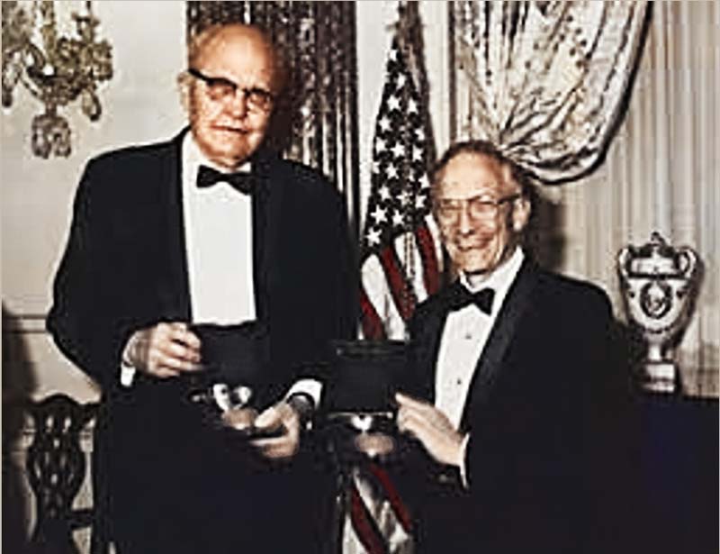
Figure 12. Rare photo of Jack Kilby and Robert Noyce together with their medals.
Noyce died in 1990, so he did not share the Nobel Prize in Physics with Kilby in 2000, but many believe he would have had he lived.
The physical insights of these two very different men were what made the invention of the integrated circuit possible. These inventors could hardly have known the outcome when they made their discoveries in 1958 — that they were going to change the world! NV