In 1970, Signetics engineer Hans Camenzind designed the 555 programmable timer chip. Fifty-four years later, it’s still going strong as the world’s largest selling integrated circuit (IC).
While we don’t use it anymore to produce old school sawtooth oscillators or modulators, it does find a solid place in microcontroller-based projects using the Arduino and Raspberry Pi.
In this article, I’ll explain the inner workings of the 555 and help make you an expert on creating your own 555-based designs.
The Basics
Despite its longevity, the 555 is largely misunderstood. Many designers rely on canned circuits from the Internet to do the job. It’s actually simple in its internals, and I’ll describe each function and how they work together. Figure 1 shows a simplified version of the internal components of the 555.
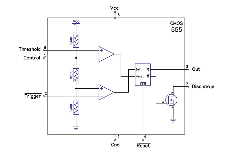
FIGURE 1: The internal components of the 555 IC including resistor ladder, comparators, and flip-flop.
The chip has two analog inputs (Threshold and Trigger), one analog input/output (Control), and two digital outputs (Out and Discharge). There are two analog comparators (see the sidebar “Comparators”) connected to three internal resistors hooked up in series.
Comparators
Comparators share the same schematic symbol as an op-amp, but work very differently:
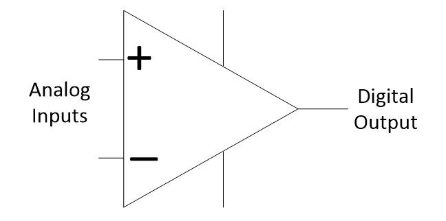
Op-amps are used for analog amplification and AC filtering, with its output being a linear voltage. Comparators have a digital output which can only put out a HIGH or a LOW, very near to the power supply rails.
If the positive (analog) input is greater than the negative (analog) input (even by a few millivolts), the digital output goes HIGH. Likewise, the digital output is LOW when negative input is higher than the positive input. Note that the positive/negative inputs do not indicate a positive or negative voltage, but the difference in voltages on the two inputs.
Inside the 555 there are two comparators. One has its positive input tied to a constant voltage of 1/3 of Vcc. The negative input is tied to the Trigger pin. When the trigger input drops below 1/3 Vcc, the output of the comparator goes HIGH. The other comparator has its negative input fixed at a constant voltage of 2/3 of Vcc. When the Threshold pin goes higher than that, the comparator puts out a HIGH voltage.
The two outputs come from an RS flip-flops’ Q and Ǭ outputs (see the sidebar “Flip-Flops”).
Flip-Flops
A flip-flop is a digital logic device that has complementary outputs controlled by two inputs. The type of flip-flop used in the 555 is called an RS flip-flop:
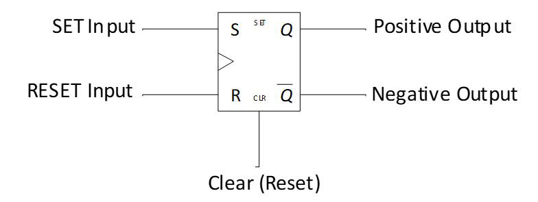
When the SET input goes HIGH, the Q output goes HIGH and the Ǭ output goes LOW. It has a sort of one-bit memory, in that the SET pin can return to a LOW or toggle many times, but the flip-flop “remembers” the last state and the outputs remain unchanged. When the RESET input goes HIGH, the opposite happens. The Q output goes LOW and the Ǭ output goes HIGH. When the CLEAR input goes HIGH, it works the same as using the RESET input.
Having both SET and RESET pins go HIGH at the same time is considered an invalid operation. The internal 555 hookup of the flip-flop prevents this from ever happening.
Note that Out and Discharge are always logically opposite of each other. So, when one is HIGH, the other is LOW, and visa-versa. The three resistors form a voltage divider. For example, with a 15 volt supply, the Control pin would have 10 volts on it (which is 2/3 of 15V) and the voltage between the two bottom resistors would be five volts (which is 1/3 of 15V). The values of these resistors (shown as 100K) don’t matter to any circuit you’re likely to design. The pinouts of the 555 are as follows:
- Gnd – Ground.
- Trigger – Active low signal normally used to start the timing function. When trigger goes LOW, the chip goes into action.
- Out – Digital output (logic HIGH or LOW). Used to output a pulse or a square wave depending upon configuration. This is where your circuit would connect to the 555 output.
- Reset – Active low signal that clears the internal flip-flop. Forces the Out pin to go HIGH and the internal MOSFET output to turn off or float (pin 7). Many designs don’t use this pin. If not used, it should be tied to Vcc.
- Control – A constant voltage output from the resistor ladder that provides a fixed voltage of 2/3 of Vcc. Some designs that override the frequency/duty cycle will input a voltage on this pin. You may also see a .001 to .01 µF capacitor on this pin. Unless your circuit is in a noisy environment, it’s not needed — especially so on the CMOS version of the 555. This pin is generally not used, so you should leave it unconnected.
- Threshold – Used to signal the end of the timing input. You can see in Figure 1 that Threshold is tied internally to the positive input of a comparator. When Threshold is greater than Control (by 2/3 Vcc), the flip-flop is set, the Out pin goes HIGH, and the MOSFET (pin 7, Discharge) turns on.
- Discharge – Open drain output of the internal MOSFET. When the Out pin is HIGH, the MOSFET’s gate input is LOW, so the transistor is turned off essentially making pin 7 float. Discharge is used to discharge the timing capacitor through an external resistor.
- Vcc – Power input. Nominal voltage range is +5V to +15V.
Don’t worry about some of these pin functions right now; we’ll get into more detail with some examples. Note that you can get a 555 IC in both single and dual packages. The dual versions usually have the part number 556 in them. Many manufacturers still make it in 8-pin and 16-pin DIP packages for easy breadboarding.
Limitations
There are a few limitations you need to aware of when using the 555:
- The original bipolar version is still made by a few companies, but they aren’t recommended for any new designs. They’re notorious for producing huge current spikes in excess of 100 mA (which causes jitter and stability problems) and need very strong bypassing to eliminate false triggers and glitches. Remember, the 555 was invented in the 1970s when DTL logic chips were common with so-called “computer grade” electrolytic capacitors with values of .1 to .25 farads. The bipolar version also has a power supply lower limit of 4.5V, so you can’t use it in 3.3V circuits. The CMOS version works fine down to 2V. The bipolar version can sink/source 200 mA, while the CMOS version can sink 150 mA and source 10 mA. This is more than enough to drive most common LEDs or relay coils. However, if you need more current than this, use a BJT or MOSFET transistor tied to the Out pin to boost current.
- You can’t use the 555 with high frequencies. The CMOS version goes up to around 1.5 MHz, while the bipolar version maxes out just below 2.0 MHz.
Free Running Oscillator
The best way to learn about the 555 is to see it in action working as a free running oscillator. This is called astable multivibrator mode. Figure 2 shows a complete oscillator made with two 4.7K resistors and one 0.1 µF capacitor.
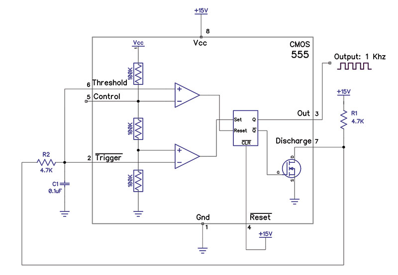
FIGURE 2: The 555 hookup for a free-running oscillator made with only three external components.
With these values, the output produces a 1 kHz square wave. Here’s how it works: When the chip is first powered up, the Discharge MOSFET is turned ON because its gate is driven HIGH by the flip-flop. So, the Discharge pin is at zero volts which travels through R2 and then to the top pin of C1. In essence, the capacitor is now shorted to ground.
The Trigger pin is also at ground, so that puts zero volts on the negative input of the bottom comparator. The comparator’s positive input is fixed at five volts (1/3 of Vcc with a 15V power supply). Therefore, the bottom comparator kicks on and puts a HIGH on the set input of the flip-flop. This causes Ǭ to go LOW, turning off the MOSFET and causing the Discharge pin to float. Q also goes HIGH, putting a logic HIGH on the Out pin.
So, the 0.1 µF capacitor is no longer being held at ground and is free to start charging up to 15 volts. One side of R1 is tied to 15 volts, so the capacitor is being charged up through R1+R2.
Now, let’s see what’s going on with the upper comparator. The Threshold pin (also tied to the capacitor along with Trigger on pin 2) was at ground before but is now seeing a rising voltage as the capacitor is charging up. The negative input of the upper comparator is fixed at 10 volts (2/3 Vcc) by the voltage divider.
Here’s where the fun begins. The capacitor continues to charge up, trying to reach 15 volts. When it reaches 10 volts (2/3 of Vcc), the output of the top comparator turns ON and resets the flip-flop which, in turn, sets the Out pin HIGH and turns off the MOSFET.
So, the whole thing repeats. C1 charges up and down continuously between 5V and 10V (1/3 Vcc and 2/3 Vcc) and does this at a rate of around 1000 Hz.
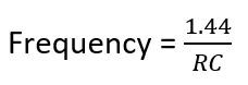
To calculate the component values needed to arrive at a desired frequency, your best bet is to use one of the many 555 online calculators where you can plug in the values of R1 and C1. If you prefer to calculate it yourself, here’s the formula:
Using the two 47K ohm resistors and the 0.1 µF capacitor in Figure 2, we get:
1.44 ÷ (47,000 + (47,000 x 2)) x .00000001 = 1021.28 Hz
The result is pretty close to 1 kHz output.
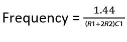
If you look at the output on an oscilloscope, you’ll see that the duty cycle is not 50%. In fact, it’s 66% HIGH and 33% LOW. This is because the capacitor is charged up through R1 and R2 in series but discharges much faster using only R2. You can tweak this a bit by using different values for R1 and R2, but you can never reach a 50% duty cycle. To achieve a true 50% duty cycle, use the circuit in Figure 3.
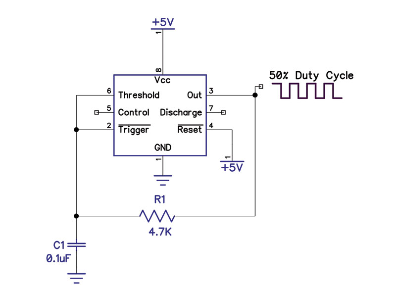
FIGURE 3: The 555 circuit that will produce a 50% duty cycle output.
Here, we charge up and discharge the capacitor through a single resistor tied to the Out pin, so the result is exactly a 50% duty cycle. Be aware though you may need to buffer the Out pin if your circuit will load it down by more than several milliamps. As an alternative, use the Discharge output with a pull-up resistor instead.
Long Time Delay
With higher value resistors and capacitors, you can do longer time delays. You might have a compressor or motor driven by a GPIO pin that can’t be cycled on and off too quickly without damage. Or, perhaps you need to turn on a relay after a long period of time. The Out pin can sink 150 mA, so if your relay needs less than that, you can drive the coil directly. The problem with creating very long time delays is you wind up using electrolytic capacitors. In higher capacitances, these parts have tolerances as bad as +80% to -20%. If you’re just building one unit, you can tweak the resistor based on the actual capacitor in use. More than one runs into a problem — perhaps two to three times difference in delay times. One solution is to use a ripple counter tied to the Out pin of the 555 as shown in Figure 4.
FIGURE 4: Setup for extending the output for longer delays using the CD4020 ripple counter.
Here, we’re using a CD4020B which is a 14-bit ripple counter. It takes 14 clock cycles before its output goes HIGH — basically multiplying any clock input by 14. Figure 4 shows a 555 with a period of 10 seconds, with its output feeding the clock line of the CD4020B producing a HIGH output 8192X slower, or around 22.7 hours.
For time delays longer than 30 seconds or so, with or without a CD4020B, you should choose a tantalum or wet-tantalum capacitor instead of an electrolytic for better tolerances and repeatable accuracy.
Hardware Debounce
While you can do switch debounce in software, there are many advantages to a hardware circuit. Your GPIO input pin will get a clean signal immediately without waiting for the debounce delay to time out. In other words, you don’t need to do dummy delays in your program waiting for the debounce period to expire. You can also use it to drive an edge triggered interrupt pin without false triggers. You can tweak the pulse width (debounce period) as long or short as you like by changing the resistor/capacitor values.
The time it takes for a pushbutton switch to bounce varies with the switch type. Figure 5 shows a tactile micro switch (right) and a chassis mount solder-lug pushbutton switch (left).
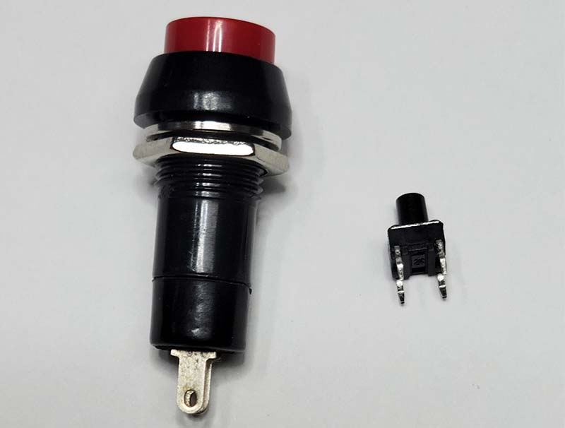
FIGURE 5: A chassis mount pushbutton switch (left) and a tactile micro switch (right). Each has very different debounce periods from 5 ms to 30 ms.
The tactile switch will usually take between 2 and 5 ms to settle down. The larger pushbutton switch will bounce as long as 20-30 ms. Most other switches fall somewhere in between. Setting a debounce period of 50 ms should cover any pushbutton switches you may have in your toolbox.
Figure 6 shows a typical debounce circuit. R1 (10K resistor) provides a pull-up for the switch so that the Trigger input gets a positive voltage when the switch is open.
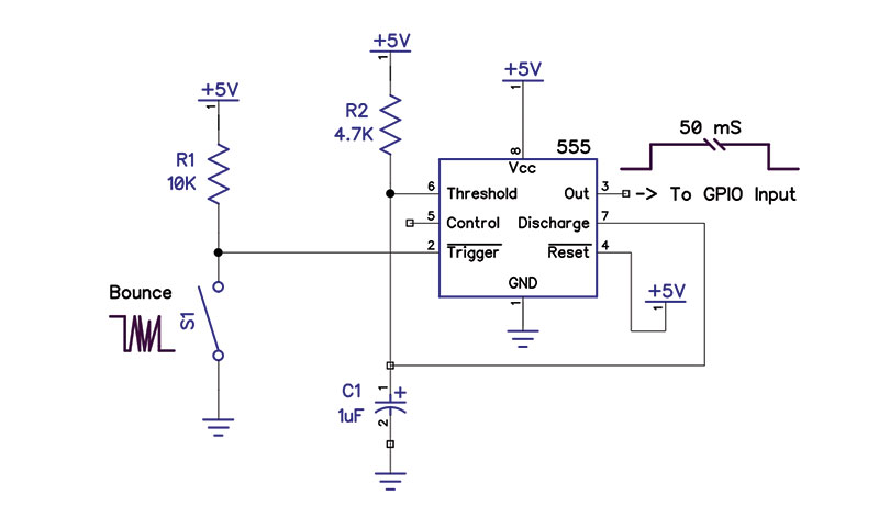
FIGURE 6: Debounce circuit to produce clean edges from noisy mechanical switches.
When the user presses down on the button, the Discharge pin floats and the Out pin goes HIGH. Now, C1 is charging up through R2. When the voltage on the Threshold pin passes through the 2/3 Vcc mark, the Discharge pin is once again floating, and the Out pin goes LOW.
This simple circuit will work as a low-cost hardware debounce for many applications. However, there are some anomalies to deal with. If the user holds the pushbutton down past the debounce period, the Out pin will stay HIGH forever until the user releases the button. If the user gets a little spastic pushing the button very quickly and faster than the debounce period, there will be multiple pulses on the Out pin.
What would work better is a single pulse on the Out pin each time the user pushes the button. It doesn’t matter how long the user holds down the button. You’ll only get one pulse or edge to serve as an interrupt input to your circuit.
Figure 7 does this at the cost of another resistor and a diode.
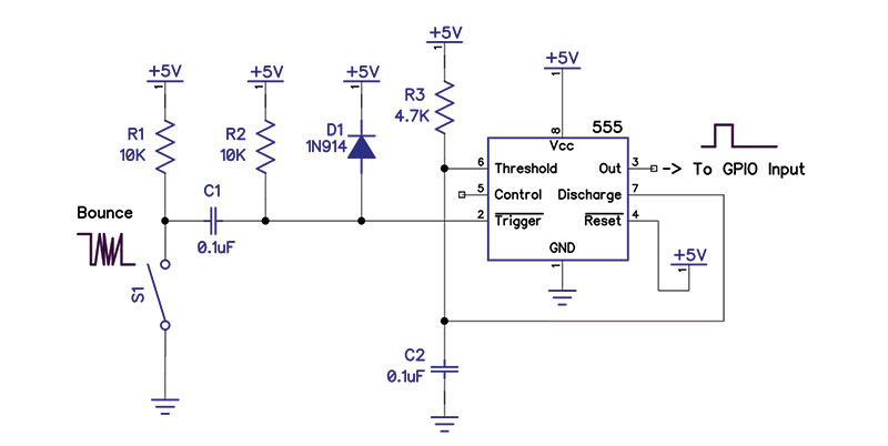
FIGURE 7: Improved debounce circuit. Output pulse width is independent of button hold time.
When the switch is open, capacitor C1 has both legs sitting at +5 volts via R1 and R2. When the user pushes down on the switch, one leg of the capacitor is forced to ground causing the capacitor to drop briefly to zero volts, then quickly charges up. This triggers the Trigger input.
If you look at Figure 8, the top (yellow) trace is the Trigger pin, while the bottom blue trace is the Out pin.
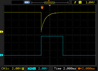
FIGURE 8: Oscilloscope traces showing capacitor charge/discharge (top) and output (bottom).
You can see the negative-going pulse when the switch is pressed, followed by the capacitor quickly charging up and a pulse being generated on the Out pin. The Discharge pin then floats and is taken out of the picture while C2 charges up through R3. At 2/3 Vcc, the pulse terminates. So, with the Discharge pin floating it stops retriggering, no matter how long the button is held down.
Just about any diode will work for D1; an ultra-cheap 1N914 signal diode is shown. The diode clamps the trigger line to Vcc (minus one diode drop), because when C1 discharges it acts like a charge pump and tries to raise the voltage beyond Vcc.
3.3V to 5V Converter
If you’re designing a project with a 3.3V main board (such as the Raspberry Pi or one of the ESP boards), it’s not uncommon to have to add a sensor or device to your project that requires five volts.
It’s easy to convert the I/O pins from 5V to 3.3V and visa-versa, but you still need a five volt supply for the sensor. Usually, you only need a few milliamps, so it’s a major overkill to have to add a second power supply.
Figure 9 shows a 555 running as a voltage doubler.
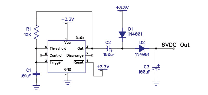
FIGURE 9: Complete 3.3V to 6V power supply using voltage doubler technique.
R1 and C1 form a free running oscillator with a frequency output of around 7.5 kHz. This part is just like the circuit in Figure 2. This drives what is called a charge pump or a Delon circuit.
The way it works is this: When the 555 Out pin is LOW, D1 is now forward-biased and puts a positive voltage on the plus side of C2, so it gets charged up. When the 555 Out pin goes HIGH, the voltage stored in C2 gets dumped through D2 (D1 is now reverse-biased) into capacitor C3. When the Out pin goes LOW again, the capacitor is charged up again.
When Out goes HIGH, the voltage is again dumped into C3, doubling its voltage. This keeps repeating, sustaining twice the Vcc voltage in C3.
The forward drop of the two diodes subtracts from the output voltage, so you don’t really get to 6.6V, but something about one volt lower. Also note that this is an unregulated supply. Draw too much current and the voltage will sag. If you only need a few milliamps, it will work fine.
If the voltage is too high, you can always add an LED/resistor to the output, or just add another diode after D2 (with its anode facing the cathode of D2) in series to drop the voltage further. If you require a regulated supply, you could put a small LDO voltage regulator on the output.
In case you’re wondering, most any electronic device/sensor will run fine on an unregulated supply, if the voltage stays within the min and max voltage rating of the device.
PWM Generator
If you need a hardware PWM generator (as in the Raspberry Pi, which only has a software PWM) or you just need an extra one, perhaps at higher frequencies than the Arduino board provides, you can put one together with two ICs, a diode, and a capacitor.
Figure 10 shows how to do it. U1 is an MCP4151 10K ohm digital potentiometer.
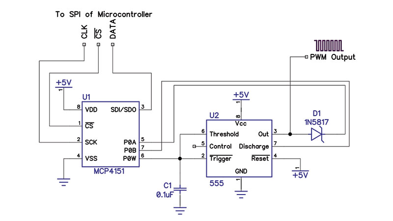
FIGURE 10: Programmable PWM generator controlled by microcontroller’s SPI signals.
It programs via the SPI interface (DATA, Chip Select, and Clock). The output of the 4151 has a programmable resistance with three legs that simulate an analog linear potentiometer. Through the SPI interface, you can set the potentiometer’s “wiper” to one of 256 resistor values. A Schottky diode (anyone will do) is connected to the Out pin. The output frequency can be determined by this simple formula:
You can also add any additional hardware such as high current drivers, or an RC network acting as a low-pass filter to change the output pulses into an analog voltage.
Conclusion
This is just a small sampling of the unique functions that the 555 timer can provide. While I focused on microcontroller applications, many more projects of all kinds are possible. I hope that I have given you enough understanding of how to use the 555 so you can design it into your next project. NV
Corrections
The first formula has a position typo and should be written as:
The text associated with the CD4020B ripple counter shown in Figure 4 should read this way:
Figure 4 shows a 555 with a period of 10 seconds, with its output feeding the clock line of the CD4020B producing a HIGH output 8192X slower, or around 22.7 hours.