David Hunter’s excellent Nuts & Volts article “Build a Pocket-Sized Altair Computer” brought back a bit of nostalgia since I too had built an Altair clone. However, I built mine in 1977. As I read his article, I was impressed by all the wonderful resources that we have today that I didn’t have back in 1977. I would like to share my experience building an Altair clone, describing some of the resources that we had and didn’t have then but we have today, and how the lack of modern resources affected my project.
To begin with, we didn’t have the Internet with all its available information. Today, we can download chip datasheets, design information, software including both source and hex code, etc. Back then, we got this information in monthly computer magazines and books. Most software available like monitor programs and Tiny Basic had source code and hex code but it was printed. If you wanted to load a hex file, it had to be done by hand on those now obsolete front panels.
The next wonder we didn’t have was Windows PCs that we could use to download source and hex files and assemble them on the PC, generate a hex file, and download to the Altair clone. Since there was no Windows PC, there was no Tera Term terminal emulator software to enter data or view results. Even CP/M computers were several years in the future.
Another service we didn’t have was the many printed circuit board (PCB) services available, not to mention the PCB layout and routing software that is common today. That left the then common construction method of wire wrapping using wire wrap sockets and a hand wrapping/unwrapping tool on perf board and plenty of 30 gauge wire.
When I set out to build my Altair clone, the first order of business was to determine the architecture of the system. That started with the definition of a bus system. I could have gone directly to the S-100 bus system in common use in those days, but S-100 prototype boards and their matching receptacles ran about $30 to $50 for a board and receptacle set. I chose to use the commonly available 6.5 x 4.5 prototype boards with interleaved power and ground traces, and a 44-pin plug and receptacle.
My bus architecture with +5, +12, -12 volt, and ground, 16 address bits, and eight data bits, plus all the necessary system controls fit nicely into the 44 available pins. I used a surplus 19 inch rack with lots of surplus 44-pin receptacles and a new 3U rack panel.
Next, I needed a source of power. Wall warts were not available — especially at the power level needed. I estimated that with all the chips I was powering, I needed at least five amps of five volt DC and one amp of ±12 volt DC. That required a large surplus 18 volt center-tapped transformer with plenty of capacitive filtering with a five volt regulator, a pass transistor, and a large heatsink. To be safe, I included a crowbar on the output.
A 24 volt center-tapped transformer and ±12 volt regulators suppled the required ±12 volts DC. Negative five volts DC was only needed for one chip, so a board-mounted five volt zener off the -12 volt pin was sufficient.
Since there was no available monitor programs already programmed into EPROMs, the only way to get code into memory was with a true front panel. My front panel (Figure 1) had 16 address LEDs and switches, eight data LEDs and switches, 10 LEDs to monitor bus indicators, and switches for Run/Stop, Run/Single Step, Single Step momentary switch, Reset, Load Address, Examine Next, Deposit Next, etc. The front panel required 29 chips, pull-up resistors, and all those switches and LEDs.
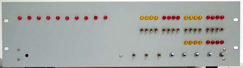
FIGURE 1. Front panel. The top two rows on the right are the 16 address LEDs and switches. The middle row shows the eight LEDs and switches. The bottom row shows the control switches. The upper left LEDs are bus control status indicators.
After the front panel was built, I proceeded to build the first 4K memory board. I built this before the CPU since I could test most of the functioning of both the memory and the front panel without the CPU. Large 256K RAMs were not yet available, so I used the then ubiquitous 2102 1K by one bit memory chip. I was limited to 4K bytes per board because 4K of memory needed 32 chips and that’s all that could fit on one 6.5 x 4.5 inch board. That required wire wrapping 32 16-pin sockets.
Note that to get the 32K bytes that are in a 256K RAM would require eight 4K memory boards or 256 2102s. Along with the 2102s were bank decoding switches and enough 74367 tri-state buffers for each address and data bit plus control bits. If I’d waited two years when the 2114 1K by four-bit memory became available, I could have fit 16K on one 6.5 x 4.5 board.
Once the memory was built and tested, I built the 8080 CPU board consisting of the 8080 CPU, the 8224 clock generator, the 8228 system controller, plus four 74367 hex tri-state buffers for address and control lines. The 8085 was not available until later, so I had to use the 8080 and all the required support ICs.
Testing required entering hand assembled hex code through the switches. All the testing programs for the CPU and memory together used about 100 instructions.
The next challenge was developing a TV and keyboard interface so I could display characters on a TV. I used Don Lancaster’s book, “TV Typewriter Cookbook” as a guide, and designed and built a 32 character per line by 16 line video interface. The available 2513 character generator created 5 x 7 characters. The 64 characters consisted of 26 all caps alpha characters, 10 numbers, and 24 special characters. No lower case was available.
Twenty eight mostly TTL ICs generated all the timing signals that put the right characters in the right place with all the TV synchronization signals, and combined them all to output a TV compatible signal to the Channel 3 TV modulator that interfaced to an old black and white TV.
Since the TV video interface took up every square inch of space on the board, I had to use a separate board for the keyboard interface. In those days, keyboards were not commonly available as they are today, but fortunately a keyboard kit was available for less than $50 that was a clone of the Teletype© ASR 33 keyboard layout. It put out eight-bit ASCII characters to an eight-bit parallel interface. The driver software detected a key press and then read out the eight-bit ASCII character.
By now, I was getting tired of entering code by hand into memory, so I needed some form of mass storage. Floppy discs at the time were quite expensive if you could find them at all. Fortunately, the industry developed the ubiquitous “Kansas City Standard” to record data on an easily available and inexpensive cassette tape recorder.
The cassette interface took eight-bit data off the address bus and fed it to a standard 8251 UART which fed a serial stream of 1200 baud data into an AFSK generator that fed audio data streams to the cassette recorder. Playback took the audio data stream from the cassette recorder and decoded it into a serial data stream which was converted back to eight-bit data bytes by the 8251 UART, and were then read by the CPU and stored in memory. It was slow by today’s standards, but it worked.
The last board to be built was an EPROM board that used the 2716 2K by eight-bit programmable read-only memory. The board had room for eight 2716 EPROMs providing 16K of storage. The 2716 PROMs available then required erasure by UV light. Electrically erasable EEPROMs were years away. Back then, obtaining an EPROM programmer was problematic, so I stayed with the cassette storage for saving and loading programs.
Every board except the CPU board had bank decoding, so each board had a separate 4K bank that it would respond to. This was done by using a four-bit decoder that was set by four DIP switches so when the top four bits of the address bus matched the four bits set by the switches, it enabled the function of that particular board.
In the end, my version of an Altair clone used seven boards (Figure 2) using a total of 143 chips including a front panel, a CPU, a 4K RAM, a 16K ROM, a TV interface, a keyboard interface, and a Kansas City Standard cassette interface — all in a standard 19” rack chassis plus a separate 10 lb power supply. If I wanted to extend to today’s 32K RAM and 32K ROM with the then available components, it would have required an additional 310 chips.
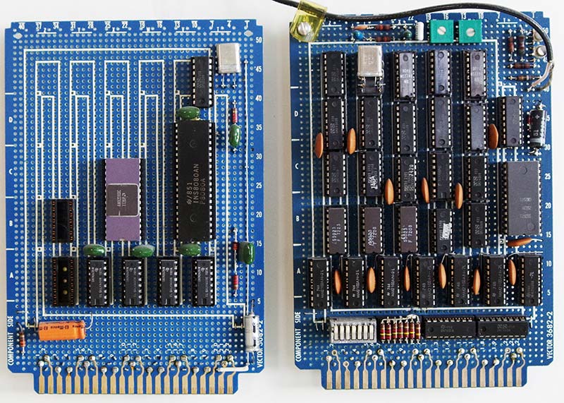
FIGURE 2. Sample cards. The card on the left is the 8080 CPU board. The card on the right is the TV video interface.
In addition to the test software, I needed software drivers that interfaced to the TV video interface, the keyboard, and the cassette recorder, so programs developed would have access to all the devices. All together this consisted of about 300 lines of code. All code was hand assembled and converted to hex format, then loaded through the front panel switches.
I waited until the cassette interface was developed before I got serious about code development because I got tired of entering all the code each time I powered up. As soon as the cassette tape was available, all I had to do was enter the tape boot loader by switches which was only about 20 instructions.
It was a great experience 40+ years ago. I learned so much about microcomputers and particularly logic design with the relatively new TTL ICs. However, I think I’ll order David’s Altair clone kit and have some fun! NV
Don Lancaster’s Cookbooks are available as free ebooks at https://www.tinaja.com.