DC-to-DC (DC-DC) converters are a common part of modern electronics. The need for an “odd” voltage can arise for biasing, backlighting, analog components, communications, or — as in the case of the LP130 discussed in a previous article — programming and verification. If your main circuit is powered from +5V and you have a few chips that need 3.3V, a simple linear regulator will suffice. However, linear regulators can only reduce the supplied voltage.
Most practical DC-DC converters are a type of switching regulator and in this article, DC-DC converter means a switching type of regulator. Switching regulators are ideally comprised of a switch (transistor-switch) and storage elements (inductors and capacitors) in different electrical configurations. Ideal switches, inductors, and capacitors have no resistance, so DC-DC converters can theoretically operate with 100% efficiency. Of course, there are no ideal components, but a DC-DC converter can still operate with higher efficiency than linear regulators (producing less heat). Plus, they can do things that are impossible for linear regulators like increasing or inverting the supply voltage.
The tradeoff for this increased efficiency and flexibility is a more complex circuit and more circuit board area. IC manufacturers have done their best to supply designers with all the active components of a switching regulator on one chip. I’ve used the UA78S40 (or LM78S40) universal switching regulator subsystem shown in Figure 1 for years because it can accommodate all switching regulator configurations.
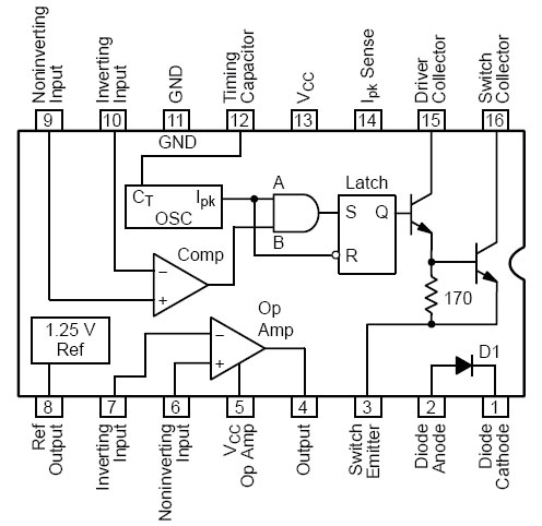
Figure 1. The 78S40 pin-out showing the internal functional blocks of the chip.
The UA78S40 is a switching regulator subsystem, consisting of a temperature compensated voltage reference, controlled duty cycle oscillator with an active current limit circuit, comparator, high current and high voltage output switch capable of 1.5A and 40V, pinned-out power diode, and an uncommitted operational amplifier which can be powered up or down independent of the IC supply.
Switching Regulator Configurations
This article will not go into details on the theory behind all the configurations. There are lots of online resources that already do a great job on switching regulator theory. I will, however, touch on the layout of the three basic configurations and one hybrid, and generally describe the concept of each.
Inverting Converter
Figure 2a (below) shows the ideal configuration for an inverting DC-DC converter.
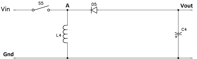
Figure 2. DC-DC converter configurations for: a) inverting converter; b) buck converter; c) boost converter; and d) buck/boost converter.
When switch S5 is closed, current flows through inductor L4 and the voltage at A equals Vin. Current flows through L4 but not to Vout because diode D5 is reverse biased. When S5 opens, the current through L4 begins to decrease, thus the voltage across L4 must reverse polarity and, because the bottom of L4 is grounded, the voltage at A becomes negative. Current flows from Vout through D5 toward A as long as A is more negative than Vout. C4 charges to a negative voltage and filters the negative pulses to produce a constant negative voltage.
Buck Converter
The buck (or step-down) converter produces an output voltage less than the input voltage. Figure 2b shows the ideal buck configuration.
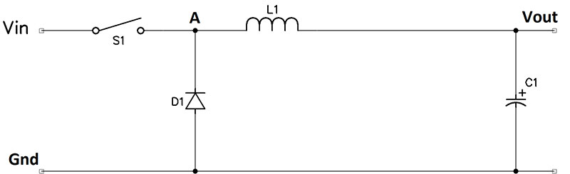
Figure 2b.
Conceptually, it’s easiest to think of the buck converter as an LC filter composed of L1 and C1. S1 provides a variable duty pulse train to the filter which averages the pulses, producing a DC output voltage proportional to the duty cycle of S1.
Boost Converter
The boost (or step-up) converter produces an output voltage greater than the input voltage. Figure 2c shows the ideal boost configuration.
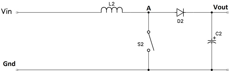
Figure 2c.
When S2 is closed, current flows through L2 storing energy in the magnetic field; D2 is reverse biased and no current flows through it. When S2 opens, the polarity of L2 reverses because the left side of L2 is held at Vin, so the voltage at A becomes greater than Vin. Current then flows through D2 charging C2 which also filters the positive pulses and produces a constant voltage greater than Vin.
Buck/Boost Converter
The ideal buck/boost converter is shown in Figure 2d.
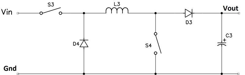
Figure 2d.
It’s the combination of the buck and boost configurations shown in Figures 2b and 2c. When S3 and S4 are closed, current flows through L3 storing energy in the magnetic field; this action is identical to the boost configuration. However, unlike the boost configuration, when S3 and S4 are open, the output voltage comes only from the inductor, and the voltage is with respect to ground (via D4) instead of Vin. This allows the output voltage to be set to any value; thus, Vout can be less than, equal to, or greater than Vin.
Feedback Control
DC-DC regulators maintain a constant output voltage in spite of changing current loads. This is done via feedback control circuitry. The feedback control samples the output voltage (usually via a resistive divider) and compares it to a reference voltage in a comparator. If the output voltage sample is below the reference, the comparator output will go high and gate the oscillator output to the transistor switch. This will switch current through the inductor at the oscillator’s frequency which will cause the output voltage to increase until it just exceeds its intended value.
Then, the output voltage sample will exceed the reference and the comparator output will go low, turning off the gate and the transistor switch. The output voltage will then begin to decrease. When it goes below the intended voltage, the process will repeat.
Figure 3 shows the UA78S40 configured as a buck converter.
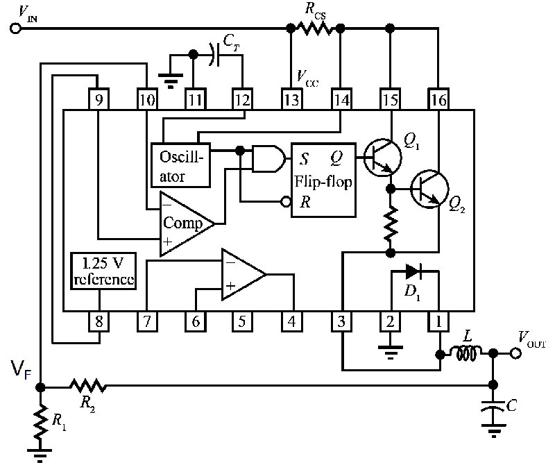
Figure 3. The 78S40 configured as a buck converter.
Rcs limits inrush current when the regulator is turned on, CT sets the oscillator frequency, and L and C are in the correct configuration for a buck converter. While these components help determine the output voltage and current capacity, they are not part of the feedback control circuit. R1 and R2 are a voltage divider that produce the feedback voltage, VF:
VF = Vout * (R1 / (R1+R2) )
The voltage divider ratio should be such that VF equals the reference voltage (VR) when Vout is at the desired value. As shown back in Figure 1, the reference voltage in the UA78S40 is 1.25 volts:
VR = 1.25V = Vout * ( R1 / (R1+R2) ), or 1.25V / Vout = R1 / (R1+R2)
The application notes listed in the Resources have formulas to design any of the fixed output DC-DC converters mentioned above based on the desired Vout, Iout, and Vin.
A Programmable DC-DC Converter
I will use the example of the LP130’s programmable Vps supply from my article in the Issue-4 2020 of Nuts & Volts. Figure 4a shows the Vps circuitry while Figure 4b shows the important functional blocks in the circuit.
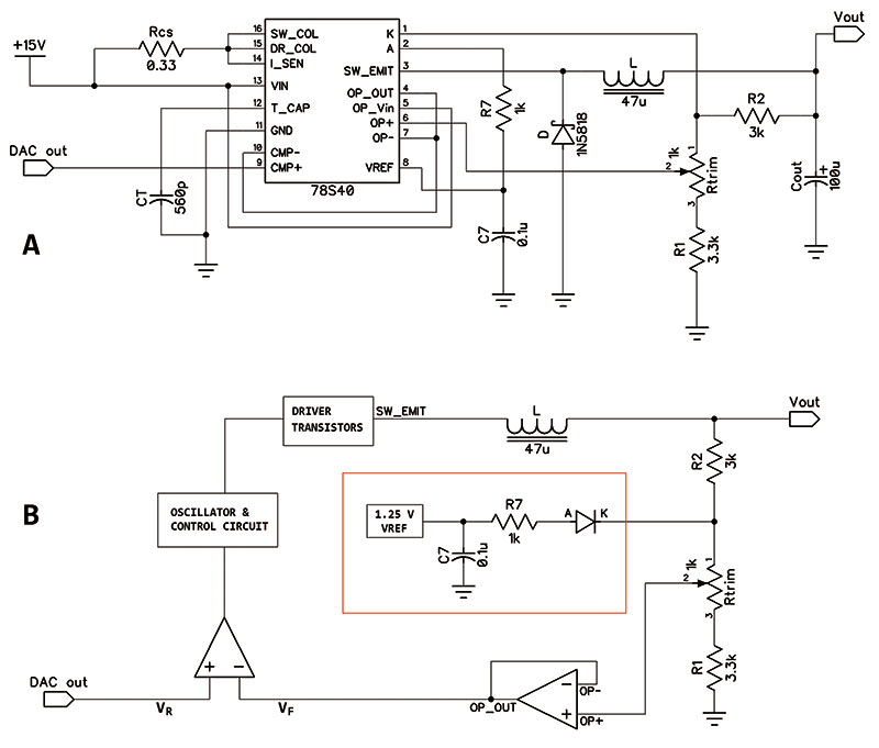
Figure 4. Programmable DC-DC buck converter used in the LP130 to generate Vps: a) circuit diagram and b) functional diagram.
Vps was designed to have a useable range from 1.8 to 7.5 volts in 0.03V steps. This variability is achieved by using a programmable voltage reference instead of the UA78S40’s fixed reference.
This programmable voltage reference could come from a linear circuit like a potentiometer or a digital circuit. In this case, I used an MCP4802 eight-bit voltage output digital-to-analog converter (DAC). The DAC’s output — which is our reference voltage (VR) — is given by the formula:
VR = 4.096 * (D / 256)
where D is the value programmed in the DAC.
For example, Vps increases 0.03 volts per step in D. To have Vps equal six volts, the steps, or the value D, that would have to be programmed into the DAC would be:
D = 6V / 0.03V = 200
The reference voltage coming from the DAC for this D would be:
VR = 4.096 * (200 / 256) = 3.2 volts
Thus, when Vps equals 6V, VR equals 3.2V, and VF must also equal 3.2V because the feedback control will work to keep VF equal to VR. As shown above in the buck converter example, the voltage divider ratio should be:
VF / Vout = VF / Vps = 3.2 / 6 = 0.533
I want the current through the voltage divider to be at least 200 uA at 1.8 volts, so the total resistance in the feedback voltage divider should be less than 9K ohms. Because I’m using 5% resistors — and 5% of 9K is 450 ohms — I want to have a 1K trimmer in the middle of the voltage divider.
Hopefully, the set point to calibrate Vps correctly will fall in the middle of the 1K trimmer, which means the equation for the voltage divider would be:
0.533 = (R1+500) / ( (R1+500) + (R2+500) )
Sparing you the intervening math, this means R2 is approximately 0.876R1. Using standard 5% resistors, I selected R1 as 3.3K and R2 as 3K. Now that the feedback resistors are determined, I could continue to select the other fixed values in the Vps circuit. Again, using 6V as a good mid-range value for Vps, I used the design equations for a buck converter from AN920 to determine the approximate L needed for this output. In this case, for Vin = 14V, Vout = 6V, and Iout = 0.5A. I found the closest standard inductor value to be 47 uH.
I then set up a spreadsheet using the design formulas for the full range of Vps voltages as shown in Table 1.
78S40 Step-down Calculations - AN920
Vin 14.000 volts
Vout Ripple 1.000% pk-pk
L 47 uH 4.70E-05
CT 560 pfd 5.60E-10 Cycle Time = 20 µsec
Ton(max) 7.000 µsec 7.00E-06 Fsw = 50 kHz
Toff(min) 1.308 µsec 1.31E-06
Vd (diode) 0.900 volts External Diode
Vsat (driver) 1.100 volts @1.5A
| Vout (volts) |
Isw(max (amps) |
Iout (amps) |
Ton/Toff |
Toff (µsec) |
Ton/(Ton+Toff) |
Vripple (Vpk-pk) |
Co(min) (uFd) |
| 8.0 |
0.730 |
0.365 |
1.816 |
7.1 |
0.496 |
0.080 |
22 |
| 7.5 |
0.804 |
0.402 |
1.556 |
7.8 |
0.472 |
0.075 |
27 |
| 7.0 |
0.879 |
0.439 |
1.339 |
8.5 |
0.450 |
0.070 |
31 |
| 6.5 |
0.953 |
0.477 |
1.156 |
9.3 |
0.430 |
0.065 |
36 |
| 6.0 |
1.028 |
0.514 |
1.000 |
10.0 |
0.412 |
0.060 |
43 |
| 5.5 |
1.102 |
0.551 |
0.865 |
10.7 |
0.395 |
0.055 |
50 |
| 5.0 |
1.177 |
0.588 |
0.747 |
11.5 |
0.379 |
0.050 |
59 |
| 4.5 |
1.251 |
0.626 |
0.643 |
12.2 |
0.365 |
0.045 |
70 |
| 4.0 |
1.326 |
0.663 |
0.551 |
12.9 |
0.352 |
0.040 |
83 |
| 3.5 |
1.400 |
0.700 |
0.468 |
13.6 |
0.339 |
0.035 |
100 |
| 3.0 |
1.474 |
0.737 |
0.394 |
14.4 |
0.328 |
0.030 |
123 |
| 2.5 |
1.549 |
0.774 |
0.327 |
15.1 |
0.317 |
0.025 |
155 |
| 2.0 |
1.623 |
0.812 |
0.266 |
15.8 |
0.307 |
0.020 |
203 |
Table 1.
As you can see in Table 1, the design formulas predict Ips = 0.514A when Vps = 6V, with Ips declining as Vps goes above 6V. In the LP130 user manual, I specify the maximum current draw for Vps should be limited to 0.5A up to 6V and decline by 74 mA/V above 6V. By limiting Ips, the filter capacitor (Cout in Figure 4a) does not need to be as large for lower Vps as suggested by Table 1.
As shown in Figure 4b, the feedback voltage coming from the trimmer is buffered by the uncommitted op-amp in the UA87S40. This helps to reduce the current flowing out of the voltage divider and keeps it more linear.
When I first breadboarded this circuit, I noticed that when VR and VF were both near zero, noise would cause the UA78S40 drive transistors to pulse on occasionally. This is not desirable because when VR is zero, the converter is programmed for zero volts. It should turn off and not pulse on occasionally. I was able to solve this problem and get Vps to do a hard turn-off with the circuit outlined in red in Figure 4b.
The 1.25V reference on the UA78S40 is routed through a 1K resistor and the power diode (A-K) on the UA78S40 which reduces it to approximately 0.55 volts. This bias voltage is tied to the top of the trimmer in the voltage divider. When Vps is off (VR = 0), the bias voltage keeps VF at approximately 0.39 volts and the UA78S40 is firmly turned off.
The bias circuit has no effect on normal Vps settings because as Vps rises above approximately 0.93 volts, the power diode reverse-biases and no current flows from the 1.25 volt reference into the voltage divider.
So, how well does this programmable DC-DC converter actually work? Figure 5 is a plot of data taken from the Vps converter on an LP130 circuit board.
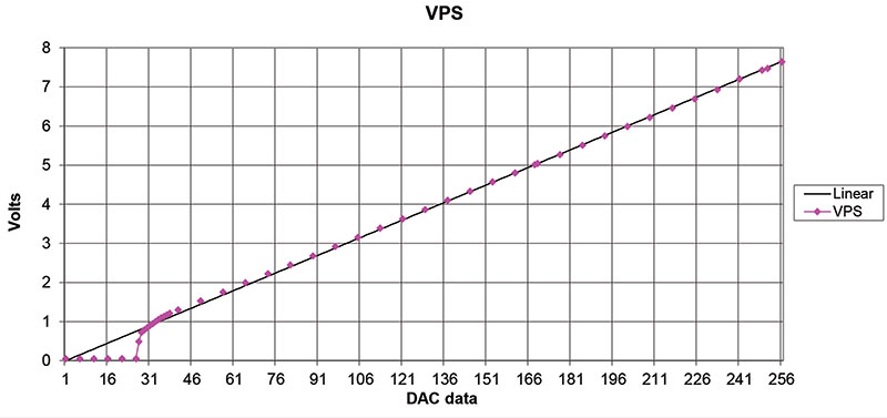
Figure 5. Measured output of the LP130’s Vps circuit plotted as Vps vs. eight-bit value programmed in the DAC.
As you can see, the bias circuit successfully keeps Vps at zero for DAC values near zero. As the programmed value nears one volt, Vps starts to climb.
Voltages below 1.8 volts are not on the linear line but from 1.8 volts to 7.5 volts, Vps is very close to the intended linear relationship of 0.03 volts per step.
Conclusion
The Vps circuit worked reliably in the LP120 and LP130. While this example was specific to the buck configuration and my requirements for Vps, the general steps are applicable to any of the configurations.
In fact, the Vpp circuit on the LP120 and LP130 is a programmable buck/boost converter.
The general steps in the design process are:
- Determine what DC input will go to the converter, such as five volts in.
- Determine your output voltage requirements, such as five to 15 volts.
- Determine the configuration you’ll need; in this case, a boost configuration.
- Determine the step size by mapping the DAC output range to the converter range. For example, if you want the maximum output of 15V at an eight-bit DAC value of 250, then your resolution is 15V/250 = 60 mV per step. You can decrease step size by going to a 10- or 12-bit DAC.
- Calculate the feedback circuit to set your DAC voltage (VR) equal to your feedback voltage (VF).
- Using the design formula from one of the application notes mentioned in the Resources, compute the required Rcs, Ct, L, and Cout for your required output current over the range of output voltages.
- Remember, you may need a bias voltage for reliable turn-off.
- Test the circuit!
I hope you find this article helpful in the design of your own programmable DC-DC power supplies. NV
Resources
UA78S40 or LM78S40 Datasheet
MC34063A Datasheet
TI
AN-711 LM78S40 Switching Voltage Regulator Applications
OnSemi
AN920/D Theory and Applications of the MC34063 and UA78S40 Switching Regulator Control Circuits
AN954 A Unique Converter Configuration Provides Step-Up/Down Functions
Maxim
Application Note 2031 DC-DC Converter Tutorial
Lucid Technologies
lucidtechnologies.info