From the digital designer’s perspective, it’s unfortunate that the real world is analog. While many low-cost microprocessors (uP) have A/D (Analog-to-Digital) inputs, I am not aware of any common and inexpensive uPs that have real D/A (Digital-to-Analog) outputs, although the Microchip PIC 1400 does have two crude 4-5 bit analog outputs. Naturally, this shortcoming is sorely missed when creating any type of analog control application, as well as many other applications.
There are two different means of simply and easily generating quality analog signals from digital signals. One method generates DC and low frequency (a few Hz) analog outputs. The other creates AC signals into the high audio-frequency range. Both methods can provide up to 10 or more bits of resolution and noise that’s 60 dB or more below full-scale. The DC/low frequency approach uses two capacitors, two resistors, and a diode. The high-frequency circuit requires only two resistors and two capacitors.
It’s important to note that the circuits provided are basic approaches. You can experiment and modify them for your own application. In addition, these procedures can employ circuits that can be changed dynamically by the uP, as required.
DC and Low Frequency Converter
In the DC and low frequency converter (see Figure 1), the first circuit converts a series of repetitive digital pulses (typically a square wave) into a DC signal. By changing the digital frequency, the DC signal can be changed, which allows low frequency AC signals to be created. For the circuit shown, the maximum useable frequency is about 10 Hz, though you could probably modify the circuit to get up to 60 Hz. This is basically a frequency-to-voltage converter.
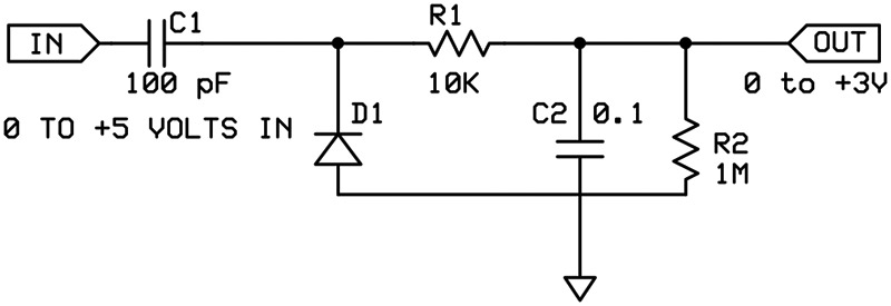
FIGURE 1. Basic circuit for DC and low frequency signals. Note that R2 can be eliminated if the subsequent circuit has a similar resistance to ground.
The operation of the circuit is straightforward. The capacitor C1 has two effects. It blocks DC and creates pulses at each edge of the digital input. The diode shorts the negative pulses to ground, which leaves a short positive pulse of about 2 uS for each rising edge of the input.
These high-frequency pulses are filtered and averaged by the RC network of R1 and C2 to create a DC signal. Resistor R2 is used to load C2. It should be a high value of about 1 to 10 MΩ, so that there is little reduction of the output voltage. It is required, however, because there is no way to remove a DC voltage on C2 once it’s there. If you want a peak-hold circuit, eliminate R2. The resistor R2 can also be eliminated if your subsequent circuit, which connects to the output, has a similar load to ground. Note that Figure 1 is a starting point that seems to work well for input frequencies of 1 KHz to 100 KHz. You may want to experiment with different values for your particular application.
How Well Does it Work?
I measured the DC output with a 1 MΩ oscilloscope probe in place of R2, and was able to get out about 0.0 volts to +3.0 volts. I say “about” 0.0 volts because that value is asymptotic. You can never get there if there is any digital signal coming in. I went down to 10 Hz and was able to measure 0.0027 volts with my 5.5 digit voltmeter. At 100,000 Hz (my highest test frequency), I measured 2.9036 volts, though you might get more voltage with a higher frequency. This is about 60% of the 5 volt operating voltage. Assuming that 0.0027 is the smallest step possible, then there are 1,075 of these steps in 2.9036 volts. This corresponds to a D/A with 10 bits of resolution. I tried ceramic, mica, and polyester capacitors and I didn’t see any significant difference.
I measured the noise with an oscilloscope. At 100 KHz, the noise was about 4 mV peak-to-peak (P-P). The P-P noise at 10 Hz was about 8 mV. (Please note that I discounted 60 Hz power-supply noise that was also present. Also, because the noise is AC and must eventually sum to zero, the DC voltage measured with the meter can be less than the AC noise. The DC meter reads a value over time, so the AC noise tends to zero itself out.) With 4 mV of noise and a 2.9036-volt signal, the signal-to-noise ratio (S/N) is 726. This is a conservative measurement because proper noise measurement should be RMS (Root-Mean-Square) not P-P. Converting P-P noise to RMS is complex and is beyond the scope of this article. But an RMS value is always less than a P-P value. So, let’s estimate the S/N ratio as 1,000. This corresponds to 60 dB or about 10 bits.
A crucial requirement of any conversion circuit is its repeatability. As shown in Table 1, the repeatability is very good. It should be noted that these tests used an inexpensive RC (Resistor/Capacitor) oscillator, rather than a uC with a crystal oscillator. So, some of the repeatability error may be due to the instability of the RC frequency. Approximately 30 minutes elapsed between the first and second measurements.
| Test Frequency |
Original Measurement |
Second Measurement |
Percent Difference |
| 100,090 Hz |
2.9036 volts |
2.9033 volts |
+0.01% (~13 bits) |
| 10,008 Hz |
1.5964 volts |
1.5952 volts |
+0.07% (~10 bits) |
| 4,000 Hz |
0.9098 volts |
0.9091 volts |
+0.07% (~10 bits) |
| 1,003 Hz |
0.2903 volts |
0.2903 volts |
0.0% |
| 100 Hz |
0.0301 volts |
0.0300 volts |
0.0% (+/-1 digital error) |
TABLE 1. The repeatability of the output voltage is very good.
The frequency response, unfortunately, is highly non-linear (see Graph 1). This may not be a problem if your design is a closed-loop. In this case, you simply increment or decrement the voltage until a proper response is obtained. However, if you want to output a particular voltage, say 2.52 volts, it’s not effortless.
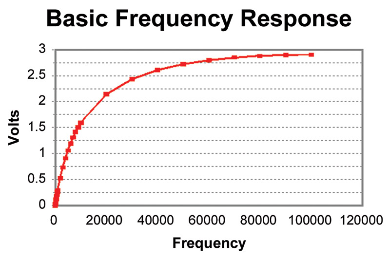
GRAPH 1. The output voltage has a non-linear response relative to the input frequency. This makes outputting a specific voltage tricky.
The crude way to obtain frequency response is to build a look-up table based on values you actually measure on a breadboard. But this is problematic, as resistors and, especially, capacitors have values that vary by several percentage points. So, there will be differences in the output voltage from unit to unit. You could tailor your uC by inputting specific values during program loading for specific components, but this is cumbersome. A better way is to use the built-in A/D that most uCs have.
During start-up or self-test (a self-test routine is crucial), you could measure the actual voltage with known applied frequencies and build a look-up table automatically. This limits the resolution to the available A/D resolution, but this may be adequate for many applications. Most uC A/D converters specify a 10K or less analog signal impedance. This is not a problem because C2 is very large relative to the A/D capacitor.
Your look-up table will probably contain about 20-40 entries, and you will interpolate between the values. This procedure reduces the memory requirements and usually provides adequate results. When you do this, you are really converting the curve to 20-40 straight-line segments. Generally, the difference between the curve and the straight line are minimal. Of course you can, and should, calculate the difference to be sure it is suitable for your application.
Frequency Modulation
DC voltages are nice, but nothing is fixed. Naturally, you’ll want to change it from time to time. The question is how quickly the DC level can change. I breadboarded a quick and dirty modulator that swept the frequency from 3,400 Hz to 175 KHz. It was supposed to be a sine wave, but if you look at Photo 1 you’ll see that the falling edge has a ledge in it. The FM frequency was about 10 Hz and the resultant signal amplitude was about 0.75 volts. You can change the values of the resistors and C2 to change the response of the circuit. You can probably get up to a useful frequency of 60 Hz, but I wouldn’t expect to go much higher.
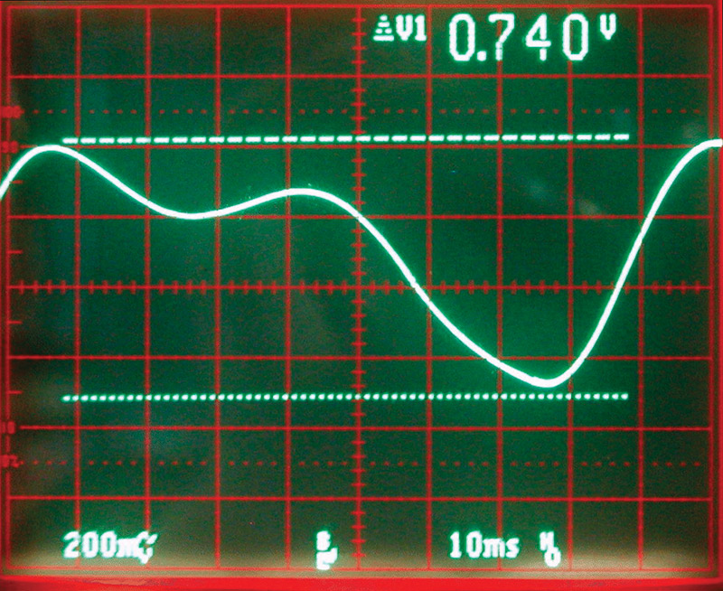
PHOTO 1. A poor attempt at an FM sine wave. However, the signal is nice and clean with no trace of digital noise.
Variations on a Theme
By changing the circuit slightly, different output voltages can be obtained. If the diode is reversed, a negative voltage is created (Figure 2a). If the diode’s anode is connected to a positive voltage (typically VCC or +5 volts) the output voltage can be about 50% greater than that (Figure 2b). This gives you great flexibility and is something that ordinary D/A converters cannot accomplish. You can output any voltage from -3 to +3 volts and from +4.5 to +7.5 volts with a standard 5-volt power supply. (There may also be enough current to supply the negative voltage requirements for an op-amp or two.)
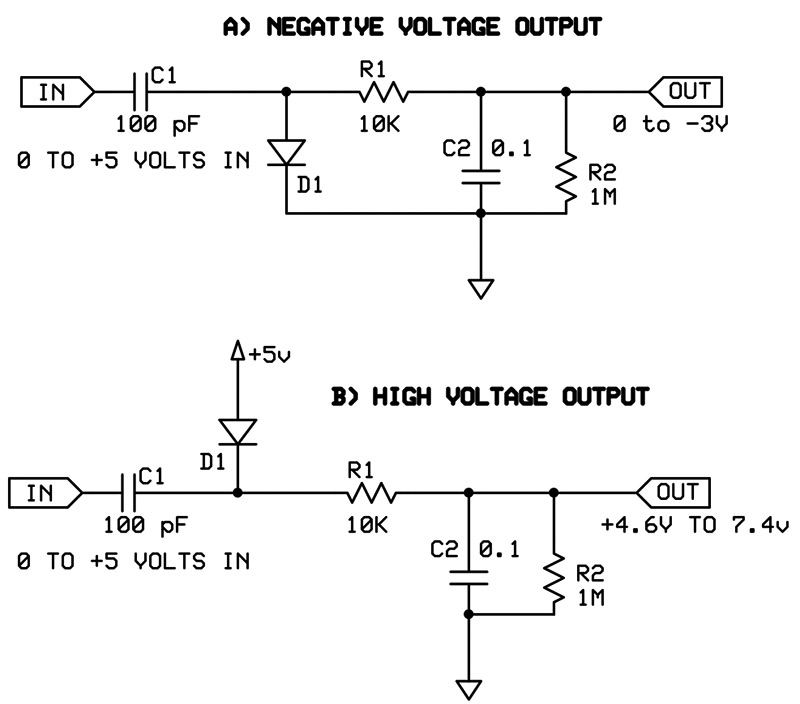
FIGURE 2. By changing the diode connections, different output voltages can be generated.
These circuits will work with any digital input. However, if you are using a uC, you can select whatever output you desire. All that is needed are a couple of free I/O pins and another diode. Figure 3 illustrates how this can be done.
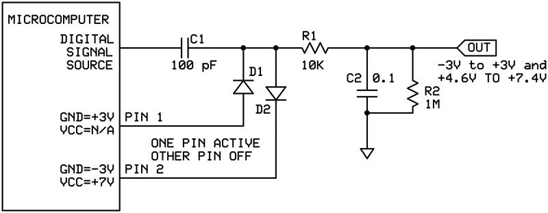
FIGURE 3. You can tri-state uC pins to effectively connect/disconnect circuit components. In this way, you can choose what output voltage you want on the fly.
The key concept is to realize that an output pin in a high-impedance state is effectively disconnected from the circuit. So, if you want 0 to +3 volts, drive pin 1 low and set pin 2 to a high-impedance state. If you want 0 to -3 volts, drive pin 2 low and set pin 1 to the high-impedance state. For +4.5 volts to +7.5 volts, drive pin 2 high with pin 1 disconnected.
The 1.5-volt dead zone between +3 volts and +4.5 volts is annoying. However, it seems that if you applied a digital signal, instead of a steady state, to pin 2, you should be able to adjust the output voltage. This is because this output would be oscillating between a positive voltage and a negative one. The capacitor C2 should average/filter this out to a DC value. By adjusting the duty cycle, you should be able to adjust the voltage, although I haven’t tried this. Additionally, you will be combining two voltages: one from the input pin and one from pin 2. This combination is probably not linear. Lastly, the frequency applied to pin 2 must be chosen properly or else it could beat/heterodyne with the frequency at the input pin and cause problems at the output. On the other hand, this might actually be a useful method of creating sine waves, but it’s not a method I’ve tried. There are many elements with which to experiment.
High Frequency Output
The second approach is completely different and a bit more subtle (see Figure 4).
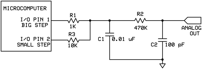
FIGURE 4. Basic circuit for high-frequency signal generation. It’s a step-hold circuit followed by a smoothing filter to eliminate the steps.
The key aspect to this approach is that the uC pin is disconnected from the circuit when in the high impedance state. Here’s how it works: The I/O pin is set to output and driven high or low for a very short time. (I used a PIC uC and a 4 MHz crystal, so these pulses were 1 uS in length.) Then it is turned “off” by making it an “input” pin with high impedance (see Photo 2).
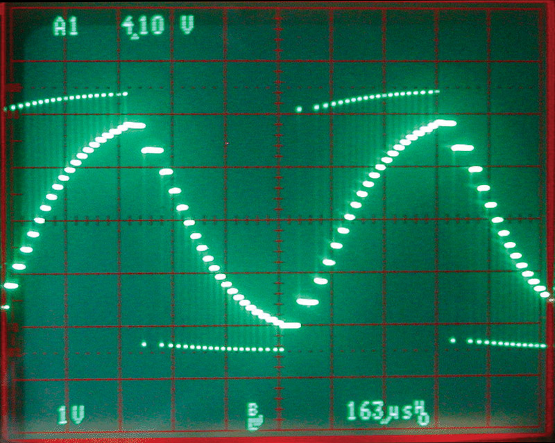
PHOTO 2. A picture of a step-hold signal taken at the uC pin (before filtering). The small pulses cause the steps, and the terraces are the capacitor holding the voltage. Another poor attempt at a sine wave.
These pulses are current-limited by R1. They pass through R1 and are applied to C1. Because these pulses are so short, relative to the time constant of R1/C1, the capacitor gets only a step charge or discharge. When the I/O pin is off, the capacitor holds the value. So, by proper stepping and holding, you can create any waveform you like (to a degree). We have an arbitrary waveform generator.
Let’s look closely at Photo 2, which is measurement at the I/O pin. The very short pulses that are near +5 volts and ground are the step pulses, when the pin is set as an output pin and driven either high or low. The relatively long terraces are the hold values when the pin is set as an input. Note that the steps are not a constant height. This is because more current will flow when there is a higher voltage difference. So, a down-step when the hold voltage is near +5 volts is much larger than a down-step when the hold voltage is near ground. You will also notice that there is a droop in the actual step voltages because of the load on the pin. In the worst case, positive step voltage sags by almost 0.5 volts. The ground step voltage rises to about 0.15 volts in the worst case. This indicates that the pin can sink current better than it can source it.
You will note that there are different lengths of time between some of the step pulses. I was trying to make a 1,000 Hz sine wave out of 40 steps. As you can see, it’s not very good. The problem is the varying step size, but we’ll come back to that later. Right now, let’s examine the last two components of the circuit: C2 and R2. These two parts make a low-pass filter to remove the step pulses and smooth the waveform. Photo 3 shows what the output looks like after it’s been filtered.
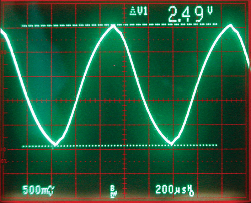
PHOTO 3. Even with the poor starting signal, the filter makes the signal look reasonable. Again, note the lack of digital noise.
Considering the input, it’s not too bad. There are 2.5 volts of a 1 KHz sine wave that has 5.6% distortion. By changing C2 to 1,000 pF, the distortion drops to 1.25% with 1.0 volts of amplitude (see Photo 4).
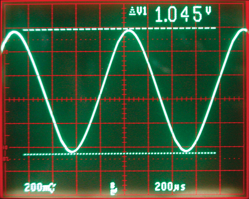
PHOTO 4. Increasing the filter capacitor makes the sine wave better at the expense of amplitude.
This looks much better. Photo 5 shows the spectrum of the signal. You can see that the third harmonic is larger than the second harmonic. This is because of the poor starting waveform.
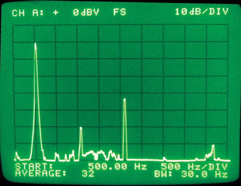
PHOTO 5. The spectrum of the signal in Photo 4 shows that the third harmonic is about 32 dB down. Again, considering the initial wave shape, it’s not too bad. No higher frequency harmonics were seen beyond the fifth (just visible at -60 dB).
Considerations
The more steps there are in the waveform, the easier it is to filter them out. I chose 40 steps because that created a very clean signal after the filter. The PIC was running at 4 MHz and was almost completely occupied with creating the waveform. The maximum speed for some PIC uCs is 40 MHz, which means that the highest frequency waveform that can be created with 40 steps is 10,000 Hz.
Unfortunately, the control registers for the I/O control of the pin are on a different page from the drive control registers. This means there is a lot of time/cycles lost in switching back and forth between pages. There are other low-cost uC manufacturers that have all the I/O registers on the same page, but the ones I saw had clock speeds in the single digits, so they will be slower.
You will note that I used a large resistor and small capacitor in the filter circuit (R2 and C2). I did this to reduce the load on the circuit as much as possible. Smaller resistors and larger capacitors can have the same frequency response, but the loading effect will be greater. This circuit also has a high-impedance output and is sensitive to loading.
The differing step sizes do have a convenient property. An equal number of up-steps and down-steps will always result in a wave that is centered at 1/2 VCC. That is, it has a DC level of 1/2 VCC. This is because the steps always get smaller as you move away from that point on any generated waveform (in sequence). If this was not the case, the DC level could shift and the wave could bump into the high or low voltage limit. This would result in a flat spot, or clipping of the signal.
Making it Better
You can change the step sizes by changing R1, because R1 controls the amount of current into C1. If you make R1 larger, the steps are smaller, and vice-versa. Photo 6 shows that the steps get much smaller and more consistent when R1 is increased to 10K. However, the wave is smaller in amplitude.
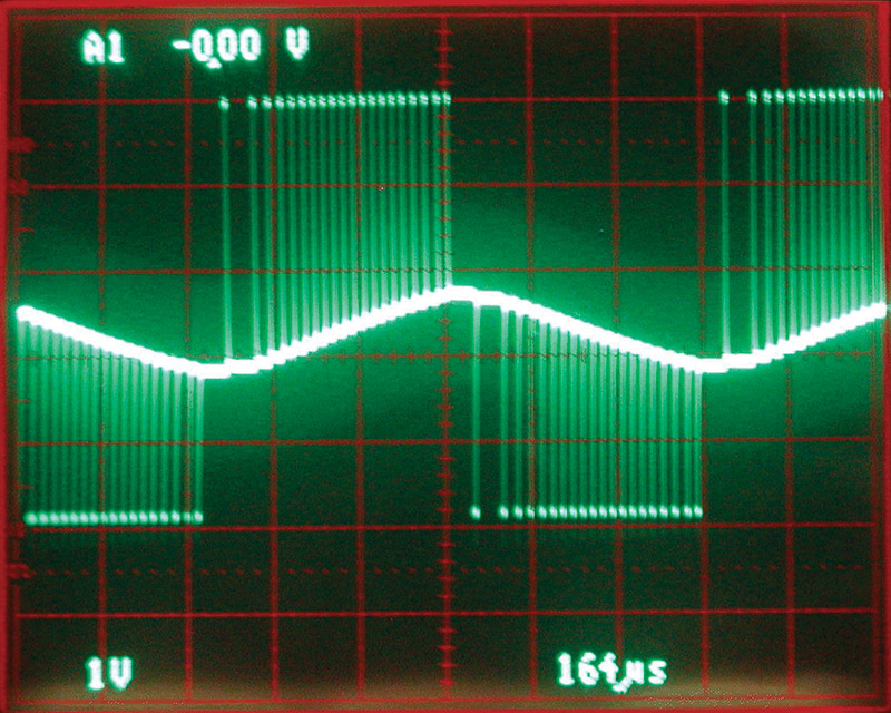
PHOTO 6. Using a 10K resistor for R1 instead of 1K results in small steps. By choosing large or small steps, the problem of inconsistent step size can be addressed.
This means more steps for a larger amplitude, which results in a lower maximum frequency. What we really need is some way of changing the current steps at will. In this way, we can use low current steps when there is a large voltage difference and large current steps when there is a small voltage difference.
Figure 5 shows how this can be done. As before, only one pin is on at a time. The other one is set to a high-impedance state.
FIGURE 5. High-frequency circuit with big and small steps. This helps compensate for the inconsistent step-size of the basic circuit.
By selecting which pin is driving the circuit, you can choose the size of the step. Of course, you can use as many different step sizes as you like. This means that the waveform can be defined as precisely as you like. The better defined the waveform, the less distortion there is.
With low frequency signals, C1 may start to discharge or droop due to internal leakage. This can be reduced with a good quality capacitor. Alternatively, you could switch a larger-value capacitor into the circuit.
Conclusion
Getting good analog signals out of digital ones can be done fairly easily with a minimum of parts. It does take some programming effort, and high-frequency audio signals require most of the uC clock cycles. However, the two general approaches described have a number of very useful characteristics. Additionally, the procedure that allows components to be switched in and out of your circuit permits you to dynamically change your circuit as required. If you experiment with these methods, you will probably find more interesting applications for your projects and products. NV