Every signal begins with an oscillator — the topic of this article. In ham radio, the oscillator is a key element in generating signals, mixing them together, and extracting the information from them. Let's see how to make an audio oscillator and learn about common types of RF oscillators.
There is an old saying: “Amplifiers are oscillators that don’t and oscillators are amplifiers that do.” An amplifier is at the heart of every oscillator, as shown in the block diagram of a basic oscillator in Figure 1A. Every single oscillator — even the digital versions, multivibrators like the 555 IC, and the ones in the little metal cans — has this same basic structure: an amplifier, some feedback, and a frequency-determining filter.
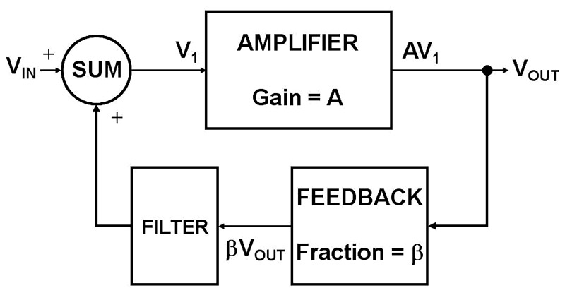
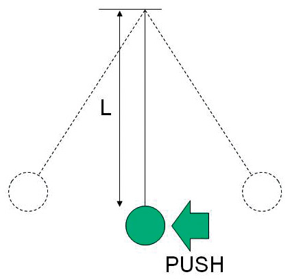
FIGURE 1. The block diagram (A) describes an oscillator as three circuits: one providing gain and the other two feeding back a fraction of the output signal into the input through a filter. B shows a pendulum which is a mechanical version of the system in A.
Figure 1B shows a pendulum which is an example of a non-electronic oscillator.1 Given a push, the pendulum will swing back and forth at a constant frequency until friction and air resistance bring it to a halt at the rest position in the center. The frequency-determining element of the pendulum oscillator is its length, L. (Interestingly, the mass of the pendulum doesn’t matter!)
The amplifier is whatever delivers the push — such as you. Obviously, the amplifier has lots of gain because you are very strong! By delivering feedback in the form of just the right strength push at just the right time, you can keep the pendulum swinging forever — or at least until dinner.
Switching back to Figure 1A, let’s imagine an electronic circuit in each block. The idea is for some fraction, ß, of the amplifier’s output signal to be fed back and reinforce its input signal. That input is then amplified with some fed back, so that the output eventually becomes self-sustaining; this is called oscillation. Furthermore, to get oscillation only at the design frequency and not just produce random noise, the system must include a filter to provide selectivity; meaning that its response is dependent on frequency. The filter can be an LC circuit, a crystal, or a timing circuit — something that is time- or frequency-sensitive.
All this creates two requirements for our general-purpose oscillator: First, the amplifier has to have enough gain at the oscillation frequency to overcome losses in the feedback circuit. Second, the filtered signal fed back to the input has to arrive with just the right phase so as to reinforce and not cancel the input signal.
These two conditions make up the Barkhausen Stability Criterion2:
Loop gain =|Aß| = 1
and
Loop phase shift = ∠ß = 0°, 360°,
720° ... 360° x 0, 1, 2, etc.
(The symbols | | mean “magnitude of,” and the symbol ∠ means "phase shift of.” If you are working with radians instead of degrees, the loop phase shift requirement is stated as ß = 2πn, with n being an integer value.)
So, just how does the oscillator start up? Noise! Random noise at the frequency for which the phase shift is just right builds a little bit more around the loop each time. Noise with a phase that isn’t just right eventually dies out because it is not reinforced. As a result, the output builds up to a sine wave at the desired frequency.
To keep the oscillator from building up to an infinite output voltage (or trying to), the circuit is usually a little non-linear so that loop gain stabilizes precisely at one when the output reaches the desired voltage.
A Phase-Shift Oscillator
Gain is easy to obtain over a wide range of frequencies. What about phase shift? The required phase shift of 360° can be distributed around the circuit. For example, if the amplifier is an inverting amplifier, it contributes 180° of phase shift. This leaves the remaining 180° to be created in the feedback circuit and/or the filter.
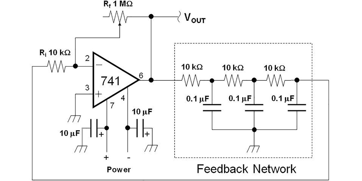
Figure 2 shows a phase-shift oscillator. To be sure, there are other circuits with better performance, but this one is the closest to the basic circuit we’ve just discussed.
Let’s start with the feedback and filter circuit formed by the three pairs of 10 KΩ resistors and 0.1 µF capacitors. Each pair forms a low pass RC (resistor–capacitor) filter that shifts the phase of the input signal from 0° to 90° as frequency is increased. At some frequency, the phase shift will be 60°.
The frequency at which each RC section contributes 60° of phase shift is:
f = (tan 60°) / 2πRC = 1.73 /
6.28 RC = 0.28 / RC
For our combination of 10 KΩ and 0.1 µF, that frequency is 275 Hz. When three identical sections are cascaded, each contributes its own 60° of phase shift, making up the remaining 180° to form a 275 Hz oscillator.
At the frequency for which 60° of phase shift occurs, the filter also reduces the amplitude of the input signal by half. If three sections are connected back to back, then the total reduction in signal level is 1/2 x 1/2 x 1/2 = 1/8 = 0.125, which is our value of ß. To make |Aß| at least 1, A must then be at least 8, and that is controlled by the ratio of Rf to Ri. Rf is made variable to allow for adjustment in gain to account for component variations and other effects as we shall see.
Building a Phase-Shift Oscillator
For this circuit, you will need a power supply that can provide both positive and negative DC voltages of 6V to 12V. Since current draw is low, you can use batteries to provide power. An oscilloscope (stand-alone or sound-card based) is required to see the waveforms produced by the oscillator and to make adjustments.
- Start by building the circuit of Figure 2. The 10 µF capacitors filter out noise to prevent feedback through the op-amp power supply pins. Set the 1 MΩ potentiometer for the highest resistance between its connections. A 10-turn trimpot will be the easiest to adjust, but a single-turn panel pot will work if you use a knob to make adjustment smoother.
- Connect power; you should see something that looks like a square wave at the output of the op-amp. This shows the op-amp output swinging back and forth between the power supply voltages as the circuit’s gain of 1M/10K = 100 is too high for the current in Rf to balance that coming through Ri from the feedback network. As a result, the output jumps between the power supply voltages.
- Reduce the potentiometer resistance to obtain an undistorted sine wave that peaks a volt or so below the power supply voltages as seen in Figure 3. (This may be a touchy adjustment with a single-turn pot.) If you have a dual-channel oscilloscope, observe the input and output voltages of each RC section, and verify that each contributes approximately 60°.
- Measure the period, T, of the output waveform (one complete cycle) and calculate the frequency of the oscillator (f = 1/T). Measure the resistance of the potentiometer (Rf) after removing it from the circuit. Compute the magnitude of the amplifier’s gain (|A| = resistance / 10 KΩ).

FIGURE 2. The phase-shift oscillator circuit. Each pair of 10 KW resistors and 0.1 µF capacitors in the feedback network adds 60° of phase shift at the frequency of oscillation.
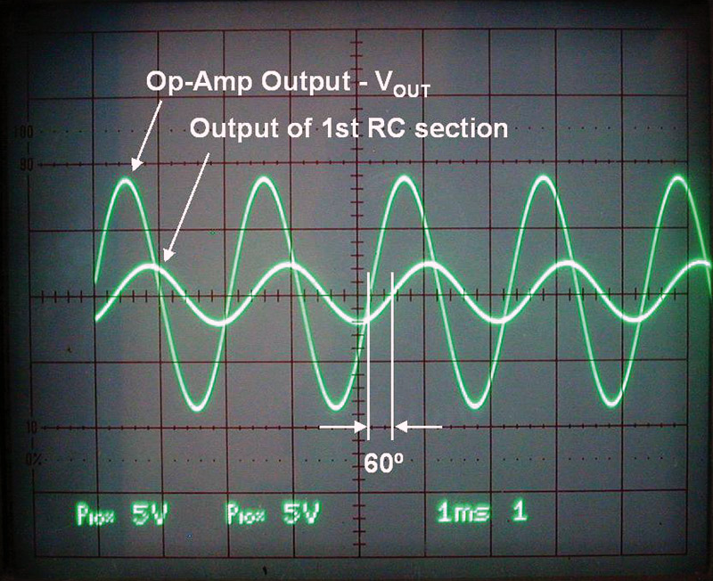
FIGURE 3. The oscilloscope traces show the output signal from the op-amp and the smaller phase-shifted signal at the output of the first RC filter section.
You probably observed that the frequency was a lot different than the initial calculation of 275 Hz — my oscillator’s frequency was 476 Hz. The voltage drop across each RC filter section was probably greater than half. My sections reduced the output to about 0.27 of the input. The gain of the amplifier will also be found to be greater than eight to compensate for that extra reduction. My potentiometer’s resistance was 603 kΩ, for a gain of 60.3 — approximately equal to 1 / (0.27 x 0.27 x 0.27).
These discrepancies result primarily from things we overlooked in the design process. Each RC section does not contribute exactly 60° of phase shift because it is loaded by the next section in the network. That causes an extra voltage drop and phase shift. The op-amp also contributes its own small amount of phase shift, meaning that the total phase shift needed from the feedback circuit will not be exactly 180° at the frequency of oscillation. These two effects result in a higher frequency for the actual circuit at which |Aß| = 1.
To see the effects of op-amp gain limitations at higher frequencies, change the feedback capacitors from 0.1 µF to 0.001 µF, increasing the 60° phase-shift frequency for each RC section to about 27.5 kHz. At this frequency, a 741 op-amp can’t cause its output to change rapidly enough to create a sine wave. (The maximum rate at which the op-amp can change its output voltage is called the slew rate, which is measured in V/µsec.) As a result, the output waveform will change to something that looks more like a triangle wave — no matter how you adjust the amplifier gain.
The phase-shift and voltage drop errors caused by the loading effects of each RC section can be eliminated by adding a buffer amplifier between each section. Replace the single op-amp with a quad op-amp such as the LM324. One op-amp section will replace the existing LM741. Add a voltage follower between each RC section with an op-amp’s output connected directly to its inverting input, and connect the input signal to the non-inverting input. (This circuit is shown as Figure 7 in the Texas Instruments applications note, Design of op-amp sine wave oscillators.3)
Because the voltage follower presents its very high input impedance to the preceding circuit, each RC section can act more like the ideal filter we envisioned during the design process.
The resulting frequency of oscillation and the gain required to achieve oscillation should change to be within 20% of the originally calculated values. (The tolerance of most 0.1 µF and 0.001 µF capacitors is typically 10% to 20%, allowing a lot of variation as well.)
RF Oscillators
The circuits used in RF oscillators are different than those used for lower frequencies. RC phase-shift circuits aren’t generally used above a few MHz. The values of R or C become impracticably small, which leaves the oscillator susceptible to stray resistances and capacitances that compromise stability and consistency. In the MHz range, it’s much easier to use inductors and capacitors to form the phase-shifting circuits which are referred to as resonators.
Most RF oscillators use discrete devices such as a bipolar transistor or FET since most integrated op-amps aren’t designed to have the necessary gain at high frequencies. Of more practical concern, a high gain wide bandwidth op-amp is much more expensive than discrete transistors such as the 2N3904 (bipolar NPN) or J310 (N-channel JFET).
Those parts cost mere pennies and have gain at frequencies up to several hundred MHz. As a result, at RF above 1 MHz, the most effective circuits use a transistor amplifier with feedback and the required phase shift provided by a resonator such as a parallel LC circuit.
Meet Hartley and Colpitts
Back in the 1920s, two fellows by the name of Hartley and Colpitts came up with the different circuits in Figure 4 that became popular in radio designs.
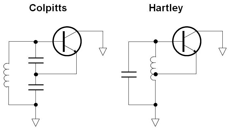
FIGURE 4. The Colpitts and Hartley oscillators work on the same principles but use different connections to the LC filter and feedback circuit, which is called a resonator. (Biasing circuitry is omitted for clarity.)
In each, the feedback is provided by routing part of the emitter circuit through a voltage divider created by two reactances (L or C). If the reactive divider is a pair of capacitors, it’s a Colpitts oscillator.
If the reactive divider is a pair of inductors or — more frequently — a single inductor with a tap part way along the turns, the circuit is a Hartley oscillator. These same circuits are in wide use today nearly 100 years later!
The Hartley and Colpitts oscillator circuits are very similar in behavior, but their differences influence the designer’s preferred choice. For example, the Hartley has a wider tuning range and fewer components than the Colpitts.
The Colpitts, however, is less expensive because it avoids the tapped inductor, and has several popular variants with good stability. We’ll cover RF oscillators in more detail in the next article.
Prototyping at RF
Most electronics builders and experimenters are very familiar with solderless breadboards. They’re very convenient and easy to work with for a variety of circuits, but they aren’t very good for analog circuits at frequencies above a couple of MHz.
The strips of contacts add too much capacitance to the circuit in unpredictable ways; the wires and leads of the components start to get long enough to have significant amounts of inductance; and controlling your grounding can be very difficult.
Hams have come up with an excellent substitute for working with RF circuits called “ugly” or “Manhattan-style” construction. In this style of prototyping, a blank piece of copper-clad printed circuit board (PCB) is used as a ground plane. Components needing a ground can be soldered directly to the ground plane.
To create ungrounded junctions ugly style, high value resistors (typically, 1 MΩ or more) are used as standoffs, costing only pennies. In addition, Manhattan-style uses small pads of PCB material as isolated connection points.
The pads are either soldered to the ground plane (requires double-sided PCB pads) or hot-glued to the ground plane.
Figure 5 shows a typical “ugly construction” example. This is a Hartley oscillator for the amateur 40-meter band around 7 MHz. In fact, I used a telegraph key to turn this oscillator on and off, making a couple of “QSOs” or contacts with nearby hams using the few milliwatts of power (also known as QRP power) from this mighty peanut whistle!
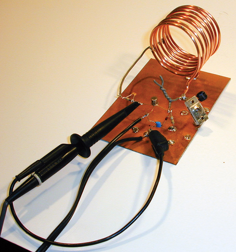
FIGURE 5. A typical RF prototype using “ugly” construction in which ground connections are made directly to the copper PCB ground plane. This is a Hartley oscillator for the amateur 40-meter band around 7 MHz.
If you are envisioning doing some RF building yourself, an RF prototyping board is a useful workbench addition. You’ll need a large piece of single- or double-sided PCB (at least 8” x 8”) and a thick piece of wood as big as or slightly larger than the circuit board.
Drill mounting holes in the corner of the PCB and attach it to the wooden base with wood screws. This gives you a large surface on which to work, plus the base makes it heavy enough to not be dragged about by test leads and cables. I attached rubber feet to the bottom of my wooden base.
Once you’ve finished (and before each use), scrub the board with a Scotch-Brite™ pad to remove fingerprints and oxidation. A swab with some rubbing alcohol will also clean the board of oils or greases. The goal is to have an easy-to-solder surface.
Once you gain a little experience with this type of construction for RF circuits, you’ll find it’s a quick and effective way to prototype even complex RF circuits before transferring them to an actual PCB or building them into an equipment enclosure. NV
Circuit Construction Tutorials
Learning how to build and test circuits at RF is a useful skill but it does take a little practice. Chuck Adams K7QO wrote an excellent and detailed tutorial, Manhattan Building Techniques, that can be downloaded from the QRP ME website, whose products are popular with low power ham operators (www.qrpme.com/docs/K7QO%20Manhattan.pdf). In addition, you can find all sorts of building tips and instructions by clicking the Radio Technology Topics link at arrl.org/tech-portal and in my own Circuitbuilding for Dummies Do-It-Yourself.
References
1. http://en.wikipedia.org/wiki/Pendulum
2. http://en.wikipedia.org/wiki/Barkhausen_stability_criterion
3. https://www.ti.com/sitesearch/docs/universalsearch.tsp?searchTerm=Oscillators#q=Oscillators&t=everything&linkId=1