PART 1: THEORY
Power MOSFETs (Metal Oxide Semiconductor Field Effect Transistors) have a lot of nice features that seem to be overlooked. Over the next two issues, we'll examine these useful devices and show how they can be employed to build: 1) a simple, transformerless voltage doubler that can supply amps of current; and 2) a 20 amp constant current source. The basic cost for parts will be about $15 for each project.
Power MOSFET Basics
Power MOSFETs (HEXFETs are International Rectifier's trademarked name for their products) are typically used in power switching applications and are classified as transistors. They have three leads like a transistor but are voltage in, current out devices. This is because the gate is completely isolated from the rest of the device. No significant DC current can flow from the gate to either the source or drain. Instead, the charge on the gate affects the conductivity between the drain and source. This is like the charge on one capacitor plate affecting the other plate. Typically, about eight volts will turn on the device completely. When on, the part exhibits a low resistance without any non-linear forward voltage drop as seen in bipolar transistors. Modern MOSFETs can have on resistances of less than 10 milliohms.
A little math shows that this device can handle 10 amps with one watt converted into waste heat (power = current2 x resistance). Since many MOSFETs come in TO-220 packages, no heatsink is needed in this instance. So, if the voltage is 100 volts at 10 amps, then 1,000 watts of power are switched with only one watt lost. That's 99.9% power efficiency. The IRFB-4410 has these specifications and costs about $4.50. That's fairly expensive for a power MOSFET.
The resistance in the off state is so high that it is usually not stated in the datasheet. Instead, they typically define the breakdown voltage as when 250 mA of current flows through the part. For most practical purposes, the power MOSFET can be considered a switch: either it's on or it's off. (Next time, we'll look at linear/non-switching applications.)
However, the key point is that it takes some time to go from a very high resistance to a very low resistance. This switching time determines the efficiency of the system and will be examined in more detail shortly.
MOSFETs come in two flavors: P-channel and N-channel. However, because of the physics involved, the P-channel types cannot match the low on resistance of the N-channel type. For that reason, there are many more N-channel parts available and at a lower cost. Most designs will use an N-channel device even if it requires additional effort. P-channel parts are not often seen except in special applications.
Unlike bipolar transistors, MOSFETs have a positive temperature coefficient. This means that their resistance increases with temperature. This can be extremely useful. As they heat up, they impede current flow more which tends to stabilize the system. Bipolar transistors allow more current to flow as they get hot. This increased current heats them up more so that they pass more current, which further increases their heat and so forth and so on. This is also called thermal runaway. When it happens, the transistor is usually lost — possibly along with additional downstream damage.
The positive temperature coefficient means that paralleling identical MOSFETs for additional power is relatively easy. If one device gets too hot, its increased resistance effectively pushes excess current to the other parts automatically. In fact, this is how power MOSFET are made. There are hundreds or even thousands of tiny MOSFETs connected in parallel to form a high power device.
Using MOSFETS
First of all, just because they are power products doesn't mean that they are immune to static. In particular, the gate is isolated from the source and drain by an incredibly thin layer of insulating oxide. If this layer is pierced by an Electrostatic Discharge (ESD), it can seriously affect how well the part operates. Voltage spikes above the rated gate voltage — due to poor board layout or circuit design — are also something to be avoided for the same reason.
The key concept in using MOSFETs is that the gate voltage controls the resistance between the source and drain. No real current is required for DC operation. This is seen in Figure 1.
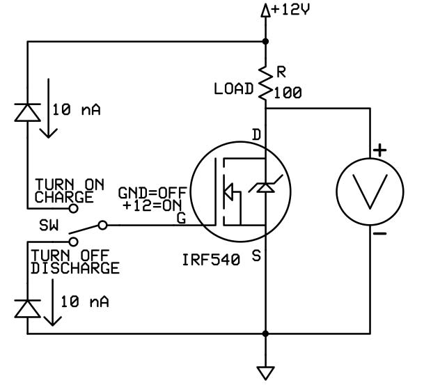
FIGURE 1. It takes virtually nothing to turn a MOSFET on and off. Here, reversed biased diodes do the job with about 10 nA of current. The voltmeter reads zero when the MOSFET is on/conducting.
Here, reversed biased diodes are used to supply the gate voltage. The current through a reversed biased 1N4148 is estimated to be about 10 nanoamps, in this instance. So, you can see that it doesn't take much to turn a power MOSFET on or off. If you actually try out Figure 2, you will see that it takes several seconds to go from off to on and vice versa. It may take much longer if the part has been in one state for a long time. Note that the meter reads zero volts when the part is conducting or "on."
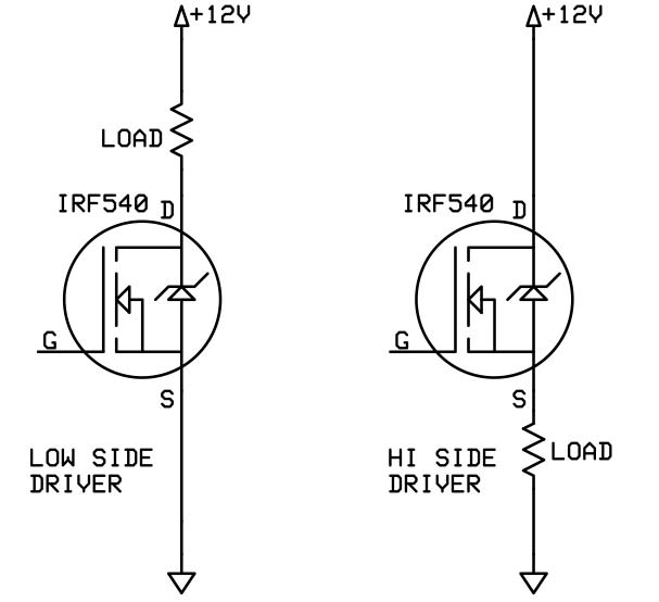
FIGURE 2. Low-side drive (Figure 2A, left) versus high-side drive (Figure 2B, right) is defined by which power supply rail the MOSFET is connected to.
The reason why it takes time to switch is because all of those paralleled and isolated gates act like the plate of a capacitor. Probably the most important characteristic of the gate is its capacitance. For the IRF540 shown in Figure 1 (which costs about $0.75), the on resistance is 0.077 ohms and the gate capacitance is 1,500 pF. Generally, the lower the on resistance the greater the input capacitance. This makes perfect sense. In order to get a lower resistance, you have to parallel more tiny devices. This means more gates and more gate surface area. This increased gate surface area translates to a larger capacitance.
This brings us to the basic practical concern in the use of power MOSFETs. In order to switch the device on or off, you have to charge and discharge the gate/capacitor quickly. If you don't, it will spend considerable time in the linear region and dissipate a great deal of heat. Therefore, to turn it on and off quickly, you have to supply a very low resistance path. This is because gate/capacitor and drive resistance combine to create an RC network.
This RC network determines how quickly the part can change state. This brings us to the perverse drive characteristics of the MOSFET. While it takes virtually no continuous current to turn the device on and off, it does take considerable pulse current to charge and discharge the gate quickly. Hundreds of milliamps or more are often needed for very fast switching. MOSFETs themselves can switch very quickly — often in 20 ns. To do so requires a powerful kick to the gate.
Other Considerations
Before we get into the drive details, it is important to mention some other points. Power MOSFETs are often used in motor-control applications. They can be ideal for this. It is imperative, however, to remember and design for inductive kickback. With high voltages and high currents, these spikes can be devastating to your circuit. They're too involved to describe here so refer to the manufacturer's application notes for guidance. This is something that they have studied in detail.
Then, there is the point of heat dissipation. Using these parts at high power can certainly result in many watts of power being generated. Many parts are rated for up to 150 watts of power dissipation. Again, this discussion on heat control is too involved. Refer to the datasheet and manufacturer's application notes.
Over-driving the gate can significantly reduce the expected lifetime of the part. For example, the IR datasheet shows that 99% of typical IRF540 parts will last about 100,000,000,000 hours (11.4 million years) with an eight volt gate drive (at 150 degrees F). Driving the gate with 20 volts reduces the time to only 1,000,000 hours (114 years).
The required drive speed depends upon the application. If you are just switching a load on and off every second or so, it doesn't really matter much if the MOSFET switches in 50 ns or 50 ms. The amount of heat generated (and energy lost) during the transition is a tiny fraction in either case. However, if you are switching at 100 kHz, a 50 ms transition time simply won't work. Even a 1 ms transition time at 100 kHz means that the MOSFET is in the linear region 10% of the total time. This will cause a significant amount of heat to be generated and a simultaneous drop in efficiency. High speed switching — especially in power supplies — is important because it allows the use of smaller value capacitors and inductors. This saves money, space, and weight.
Low-Side Driving
The simplest and most common circuit is called "low-side" driving (see Figure 2A). (Note, we will mostly limit the discussion to N-channel devices for brevity and simplicity.) In this case, the MOSFET is connected directly to ground. High-side driving (Figure 2B) places the load at ground and the MOSFET connects to the power source. To turn on a low-side MOSFET, all you have to do it raise the gate about eight volts above ground. Grounding the gate turns it off.
It is possible to use five volt TTL logic level signals (a.k.a., microprocessor) to directly drive a MOSFET. However, this won't turn the device completely on. Nevertheless, oftentimes this is sufficient. For the IRF540, a five volt gate drive will allow about 10 amps to be switched (typically) instead of the 28 amps specified. So, if your application doesn't require the full power of the part, TTL signals may work. You can always use an "open-collector" part that allows you to pull up the logic output above five volts. Also, there are special MOSFETs that are specified to operate with a five volt gate drive. Naturally, they're more expensive, but they may be worthwhile considering the additional expense and difficulty of designing a higher voltage gate drive circuit. Typically, these are identified as "logic-level" devices.
CMOS logic has the advantage of being able to operate on eight volts or more without a problem. However, they are terrible when it comes to drive current — even with paralleled outputs. Typically, they only provide a couple of mA or so per output. So, it's difficult to drive a MOSFET gate at high speed. Many applications don't need high speed switching, however.
A 555 timer works quite well as a driver. Be sure to use a bipolar part (NE555) rather than a CMOS part (xxC555) (see Photos 1 and 2).
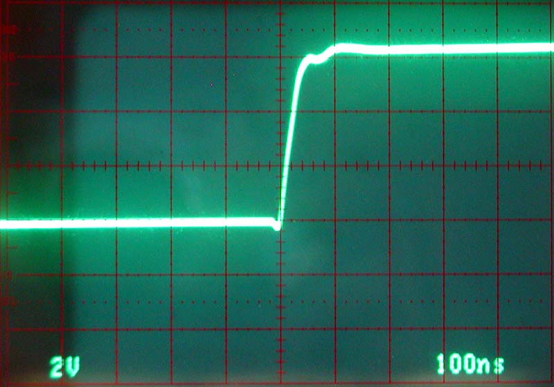
PHOTO 1. A bipolar 555 timer (Texas Instruments NE555) turns the MOSFET on and off in about 50 ns.
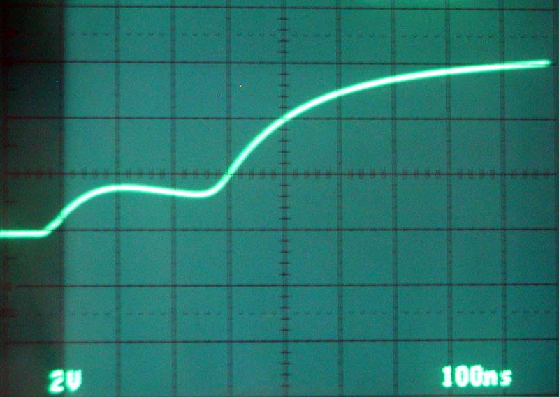
PHOTO 2. A CMOS 555 timer (Texas Instruments TLC555) takes about 800 ns to turn on the MOSFET which is about 16 times longer than the bipolar version. Turn off time is about 50 ns.
There are also many discrete transistor circuits you can use. They can be single transistor drivers as in Figure 3.
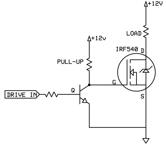
FIGURE 3. Typical low-side driver. Turn on time is determined by the pullup resistor. Turn off time is quite fast.
The drawback with this design is that the pullup resistor limits the current so the turn on speed is slower than the turn off speed. A totem pole design (Figure 4) can be very effective. You can also use a NPN/PNP design to eliminate the need for the inverter.
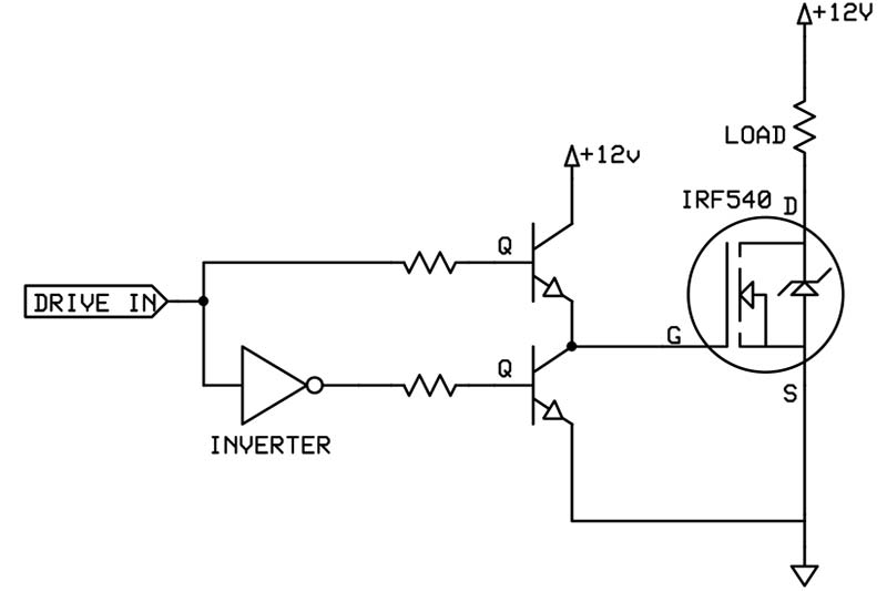
FIGURE 4. Totem-pole driver provides fast and symmetrical on and off times. A PNP/NPN design can eliminate the need for the inverter.
Lastly, there are special chips usually called "low-side gate drivers" that provide a high current for very fast switching. If you feel the need for speed, this is probably the way to go. They cost a buck or so but eliminate the practical problems of circuit design and testing. Naturally, there are high-side gate drivers, half bridge gate drivers, and full bridge gate drivers, as well. Table 1 provides a summary of typical drive speeds as measured at the load rather than at the gate. (Note that the gate driver measurement of 175 ns is suspiciously slow. Perhaps that was due to my simple test jig. Measurements of the voltage doubler circuit showed symmetrical 50 ns switching speeds. It's rated at 15 ns/1,000 pF.)
TABLE 1. Low-side drive summary (times are measured at load).
| Circuit |
Turn off time |
Turn on time |
Comments (10V D-S with 100 mA load) |
| TTL 'LS04 |
500 nS |
100,000 nS |
Can't drive fully on. Logic-level parts available. |
| TTL/pullup |
200 nS |
3,000 nS |
Speed limited by pullup 1K resistor. (74145) |
| CMOS |
8,000 nS |
1,000 nS |
Very slow but turns on all the way. Easy. (CD4069) |
| CMOS x 6 |
2,000 nS |
400 nS |
Better than above, but still slow. (CD4069) |
| NE555 |
175 nS |
60 nS |
Bipolar good, CMOS poor. (Photos 1 and 2) |
| Discreet |
400 nS |
2,500 nS |
Speed limited by 1K pullup resistor. (Figure 4) |
| Totem pole |
175 nS |
150 nS |
Very good. (Figure 5) |
| Driver |
175 nS |
50 nS |
Best speed (see text). (LM5109B) |
High Side Driving
High side driving of an N-channel part can be tricky (see Figure 2). The gate has to be about eight volts above the source voltage to turn it on. However, because of the very low resistance when it is on, there is very little voltage drop between the drain and source. Thus, the source pin voltage is often very close to VCC. So, to turn on the device you may need a gate voltage greater than VCC.
There are some ways around this problem. The first is to build a voltage multiplier. Obviously, this is not an elegant solution. A P-channel part might be the easy solution here despite the higher cost and poorer performance. Figure 5 shows the typical hook-up. Note that the source is connected to the positive voltage. In this configuration, the P-channel device will turn on with a gate voltage eight volts below the source pin. So, if VCC/source is 10 volts, the part will start to conduct when the gate drops to about seven volts and will be fully on at two volts, or eight volts below the source voltage.
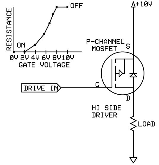
FIGURE 5. A P-channel device can be used in a high-side configuration fairly easily. The part turns fully on when the gate voltage is about eight volts below the source pin. Note that the source is connected to the positive supply rail.
If you are continuously switching the load on and off in less than a second or so, there is another approach that can be used with N-channel parts. This is called bootstrapping and is shown in Figure 6.
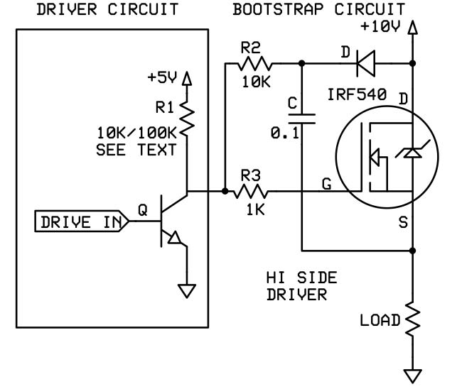
FIGURE 6. This bootstrap design increases the gate voltage but is very slow ... about 30 ms turn on time. Voltage increase is determined by the ratio of R1 and R2. R1 tends to pull any gate voltage down to five volts.
This is a modified circuit found in the Siliconix MOSPOWER Applications Handbook. The conceptual design of the circuit is subtle but fairly simple. When the transistor is on, the MOSFET's gate is pulled low and the capacitor is charged to VCC (10 volts) through the isolation diode. When the transistor is turned off, the gate drive rises to VCC because of the charged capacitor (mostly via R2 and R3). Since the MOSFET is off, the source pin voltage is pulled low through the load. This means that the gate voltage is well above the source pin voltage and the MOSFET will start to conduct. As this happens, the capacitor acts as a voltage source in series with the source pin. So, any voltage on the source pin is added through the capacitor to the gate. (The negative side of the capacitor gets pushed up by the increasing source pin voltage which pushes up the positive side by an equal amount.) In effect, the part pulls the gate voltage up by its own bootstraps.
Naturally, theory and practice are different. The capacitor should be at least 10 times the gate capacitance. In most cases, 0.1 µF will work. The diode is any power type with an appropriate voltage rating. The resistors R1 and R2 are the tricky components.
The pullup resistor (R1) determines how big the voltage increase is. This is because it connects the gate drive to the five volt supply. Any voltage greater than five volts will be pulled down to five volts through this resistor. Note that this resistor may not always be visible. For example, a 555 timer (connected to R2-R3) can supply 100 mA for an equivalent pullup resistance of about 50 ohms (at five volts). Obviously, a 10K resistor above five volts by any significant amount.
As shown in Figure 6, the 10K value for R2 only supplies 10 volts (referenced to ground) to the gate which is not adequate if the source is also at 10 volts. If R2 is increased to 100K ohms, over 17 volts is applied to the gate which is probably okay for most applications with the IRF540. Note that the turn on time is also controlled by R2 (the turn off time is controlled by R3). Charging the 1,500 pF gate through 100K takes about 30 ms to turn on the device (measured). So, you trade off speed versus voltage. The general rule of thumb is that R2 should be about 1/10 of the equivalent pull up resistor, R1.
Resistor R3 controls the turn off time and is included mostly for completeness. Oftentimes, a gate series resistor is shown. It is not necessary. As shown, the turn off time is about 2 ms. If R3 is replaced by a wire, the turn off time drops to about 500 ns.
These problems can be eliminated by using an open-collector transistor circuit which is shown in Figure 7.
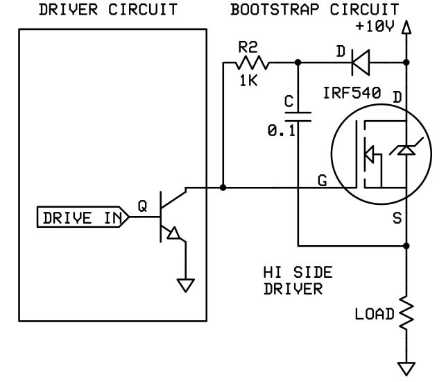
FIGURE 7. Using an open-collector design eliminates pullup resistor and gate resistor. Switching speed is much faster than Figure 6. Turn-on time is about 4 ms.
In this case, there is no connection to the five volt supply so there is no pulldown problem. This eliminates R1 and allows the use of a much smaller resistor for R2. This resistor is now chosen to limit the current into the transistor to a safe level (100 mA as shown). Resistor R3 can also be eliminated. This circuit provides about 18 volts to the gate and switching time is about 4 ms for turn on and 500 ns for turn off.
However, if you want to use a high-side N-channel part you should really consider using a driver chip. The LM5109B only costs about $1.60 and drives a high-side and low-side MOSFET in a half-bridge configuration. It's rated for 90 volts (to the MOSFET) and can turn them on and off in 15 ns with 1,000 pF gate capacitance. Considering the time and effort in designing your own high-side driver, this is a good deal. There are lots of other parts available, as well.
Conclusion
This time we've looked at power MOSFETs and found that they have some very useful attributes. They're cheap and powerful, and can be fairly easy to implement. Naturally, there are practical considerations in addition to the theory.
Next time, we'll build two projects. The first is a transformerless, high current voltage doubler using a full-bridge design that has many other useful applications (like motor control). The second is a linear, constant current power supply capable of providing 20 amps or more. NV