Many small board repairs can be done with a methodical approach using basic tools such as DMMs (digital multimeters) and oscilloscopes to measure voltages and waveforms at significant test points in a circuit. Troubleshooting modern, complex, multi-layer PCBs (printed circuit boards) is often challenging, with factors such as available documentation playing a role in the speed of repairs. Automated systems may prove cost-effective for larger repair loads. Anyone interested in electronics is bound to encounter a dead board or two, whether it’s their own or someone needing help. What’s the best approach when confronted with a PCB that doesn’t do what it’s supposed to do?
Circuit boards are more complicated to repair today than even a few years ago. Manufacturing mistakes and in-service component failures have become commonplace. Older circuit boards can malfunction due to components that fail — notably electrolytic capacitors — but new ones (assuming the layout is correct) might not work due to manufacturing errors, parts poorly or incorrectly soldered, solder bridges, etc.
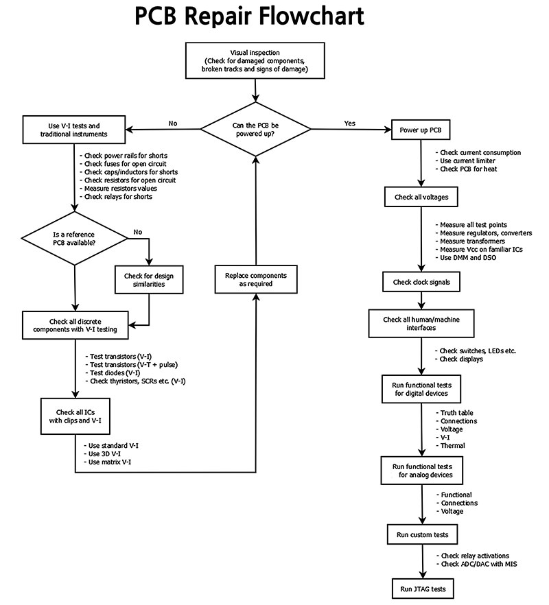
While simple soldering and component changes may be suitable for less complex fixes, some repairs may require more expert approaches to find fault causes. Repairing complete PCB assemblies can seem intimidating, but a methodical approach helps in finding and fixing problems quickly.
It’s wise to get a report from the end-user about how the board failed. Did it ever work correctly? Did they just run a software update and that killed it? Can you see any obvious fault clues such as broken wires or tracks?
Usually, it’s wise to refrain from powering up a damaged PCB at first. If, for instance, a simple blown fuse is suspected, the reason for the issue must be determined rather than just replacing the fuse (with a bigger one!). Short circuits or overloads usually leave tell-tale signs.
If the PCB has been conformally coated to keep out moisture and dust, this layer must be removed (at least at a few critical test points) before fault diagnosis can begin. Conformal coatings may need to be removed by solvents, peeling, or blasting, but a new technique is being developed whereby the coating can be pierced through with very sharp test pins (see Figure 1).
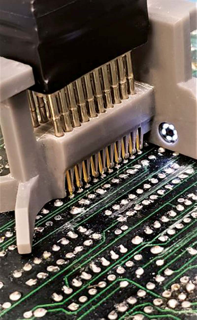
FIGURE 1. Piercing probes penetrate conformal coating.
Before commencing the repair, gather together any relevant circuit diagrams, known good boards, and appropriate test equipment such as a DMM, solder/desolder hand tools, an oscilloscope, power supplies, etc. (Figure 2), referably on a static-free bench. The most helpful “tool” to start with is the user report of how the failure occurred or what fault was observed.
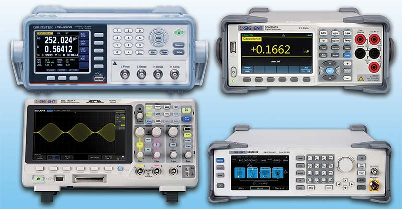
FIGURE 2. Typical benchtop instruments: LCR meter, oscilloscope, DMM, and spectrum analyzer.
The most versatile tool is the multimeter, but depending on the complexity of the PCB, an LCR meter, oscilloscope, power supply, and logic analyzer may also be needed to investigate the operation of the circuit. RF circuits may need more sophisticated tools such as a spectrum analyzer to check frequencies and signal levels.
Here are some strategies to streamline the process of reworking and repairing PCBs. Troubleshooting is also much easier if a known good board is available so that visual and signal comparisons can be made. Lack of a comparative board or documentation makes the challenge more daunting.
Visual
Check for loose connectors or components in sockets, which can often get dislodged in shipping. Look for burned or damaged parts, or solder bridges causing a short circuit of signal or power lines. This is where a high-power digital microscope is really useful (see Figure 3). Visual inspection is an essential first step in troubleshooting.
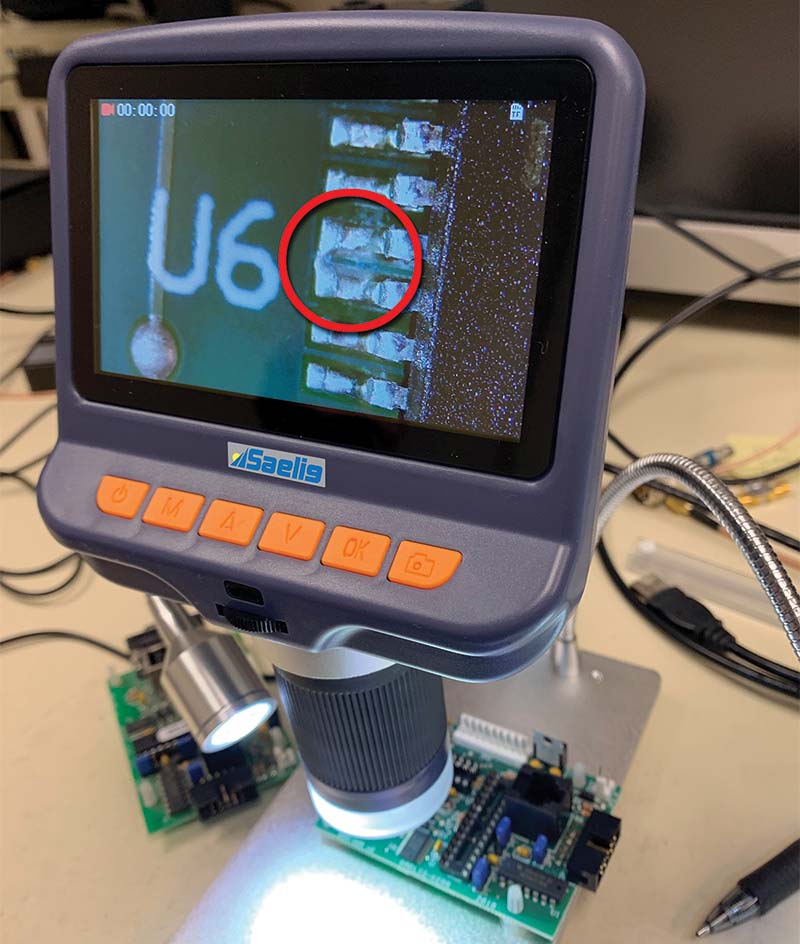
FIGURE 3. Solder bridge short circuit revealed on microscope.
Visually inspect capacitors. If leaks, cracks, bulges, or other signs of deterioration are evident, replace the capacitor with an equivalent type and voltage rating. Capacitors have a limited life and are often the cause of a malfunction.
Look for broken leads on the components. Some devices have tiny leads that can easily break off at the circuit board. IC legs can become bent during assembly. Look for cracks on the circuit board, leading to broken circuit traces or broken components.
Components or parts such as transformers, power output transistors, resistors, and capacitors that show a burn mark can be detected easily by observation. Apparent burns and brown stains (and an awful smell) can identify the overheated components, but you need to find out why they overheated.
A poor solder joint or bridge is another common item found during a visual inspection. Good solder joints always look smooth, bright, and evenly flowed. A dull surface can suggest a defective joint. Are there any solder bridges between tracks? Reversed or incorrect components?
Short circuits can be very tricky to troubleshoot. A momentary power-up test may indicate that a short exists, but often the location of the short is elusive. You can spend a long, frustrating time trying to locate a single short, particularly an interlayer short. Briefly powering up the board after spraying with freezer spray is the poor man’s way to find shorts, which will heat up an area of low resistance in power lines.
A more sophisticated method is to observe with a thermal (IR) camera to show a location that heats up more than the surrounding components (refer to Figure 4).
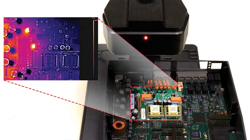
FIGURE 4. Hot spots and short circuits shown by thermal camera.
Power the rail voltage with something less than the 3.3V or 5.0V required and limit the power supply current too. Start with low volts/amps and bring both up slowly. PCBs may have a self-limited life through the poor design of excessive component heating, inadequate heatsinks, or heatsinks with dried out heatsink compound.
A quick way to find a fault is to compare the thermal images of a known good board with the device under test (DUT). Significant temperature differences can highlight the fault location. Using this approach, entire complex boards can be inspected in a non-contact manner.
Common defects such as power-to-ground shorts and bad components can quickly be found with this method. A changing or different color representation of the image may indicate overheating in a solder joint, circuit trace, or show a portion of the board that is malfunctioning.
Laboriously testing every resistor, capacitor, diode, transistor, inductor, MOSFET, LED, and discrete active component can be done with a multimeter or LCR meter, but is not an efficient way to do debugging.
Simple Tests
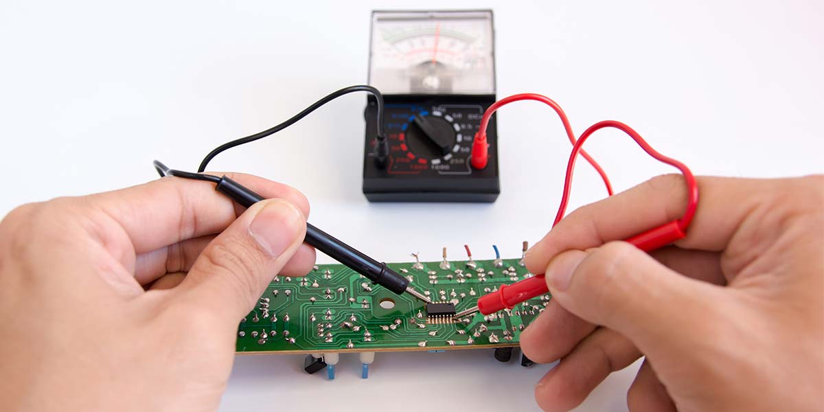
If the board can be powered up, a digital multimeter can be used to check rail voltages at ICs, outputs of voltage regulators, and obvious signals such as clocks, correct/expected logic, and I/O levels. An oscilloscope can be used to verify voltage waveforms and communications of a powered board. To check for the presence of a PCB’s Wi-Fi signal output, even a cellphone can come in handy.
Leaky capacitors can be found using the resistance setting of the DMM. Set the meter to read in the high ohms range and touch the meter leads to the corresponding leads on the capacitor; red to positive and black to negative. The meter should start at zero and then moving slowly towards infinity. With large capacitance values, the ramp will be very slow.
Note: A good capacitor stores an electrical charge and may remain energized after power is removed.
Before taking a measurement of electrolytics, disconnect the power and carefully discharge the capacitor by connecting a resistor across the leads. With the meter in the ohms setting, there will be some constant current sent out from positive to negative leads. An open cap will show open; a shorted one will show close to zero ohms.
Checking the operation of HMI interface items such as touch panels and switches may reveal functional issues due to connection or component problems.
Signal probing with a DMM or oscilloscope requires some understanding of the circuit to interpret the result, but is made so much easier if you have a known good board to compare point-to-point results. DC voltage tests start by probing with reference to ground. When checking an IC, start by testing the voltage supply pin.
Most ICs can be identified by their markings and many can be operationally tested against their published specifications using scopes and logic analyzers. Comparing the behavior of an IC to a known good one is a quick way to identify anomalous behavior.
An engineer’s favorite habit of touching low voltage parts of a circuit can change impedances which, in turn, can alter the behavior of the system (or else inadvertently find overheating!). Used in conjunction with a scope, this technique can help identify locations that need additional capacitance to remove unwanted oscillations, for instance.
Intermittent failures are the most challenging and time-consuming aspect of the troubleshooting process. Common irregular faults can be due to component overheating or degradation, poor soldering, and loose connections. Long memory in a scope can be helpful for zooming in to a signal record for finding rare events. Applying freezer spray in the right location can sometimes aggravate and identify intermittent issues.
How Do the Big Boys Do It?
Professional repair houses and repair centers that fix boards all the time need better solutions than a scope and a DMM. In situations where faulty PCBs come in a steady stream, and with the increased emphasis on efficiency and reduced costs, universal automated test systems have replaced individual test instruments. PC-based in-circuit testers perform both a powered in-circuit logical test of digital and many analog ICs, as well as V-I signature analysis of the chips, using a variety of test clips.
Automated Testing Equipment (ATE) systems that contain libraries of digital chip pinouts can assist the technician in troubleshooting, and also determine wiring patterns of the circuits if not known. ATEs can check for digital functionality of ICs, and also provide a signature analysis of both active and passive components. Unknown chips can be identified by their Boolean output.
Acquiring automatic testing equipment means that frequent repairs can be performed in-house more efficiently than sending the items to an outside service. Some ATEs can be extremely expensive and may come with a steep learning curve; meaning that after purchase, they sit idle in a storeroom. ATEs can perform automated or computerized test procedures on a DUT, including functional testing of ICs, analog and digital components, complete boards, etc.
These products vary in complexity, depending on the different levels of test capabilities required for various board needs. Computer-based automated test procedures can run reliably and consistently with test results being captured automatically, with high accuracy, at high test speeds, and with extreme flexibility.
Typical ATEs include: In-circuit testers, performing device level tests on components mounted on circuit boards; functional testers, used to test full functionality of boards and modules via edge connectors; and boundary scan testers for products that are JTAG-compliant such as BGA, FPGA, CPLDs, or even complete boards with a JTAG connector.
An example of an ATE PCB repair system is the ABI Electronics System 8: a board test system that uses a selection of CD-drive size modules to create a customized PC-driven PCB test station (Figure 5).
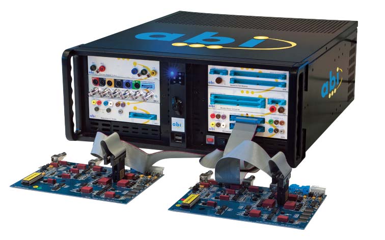
FIGURE 5. ABI System 8 automated test equipment.
Built in a PC case or 19” rack-mount, System 8 is a mix-and-match set of test instruments to suit most testing and fault-finding needs. Comparing results from a known good board with automated-sequence fault-finding procedures, fault diagnosis becomes possible by minimally trained staff.
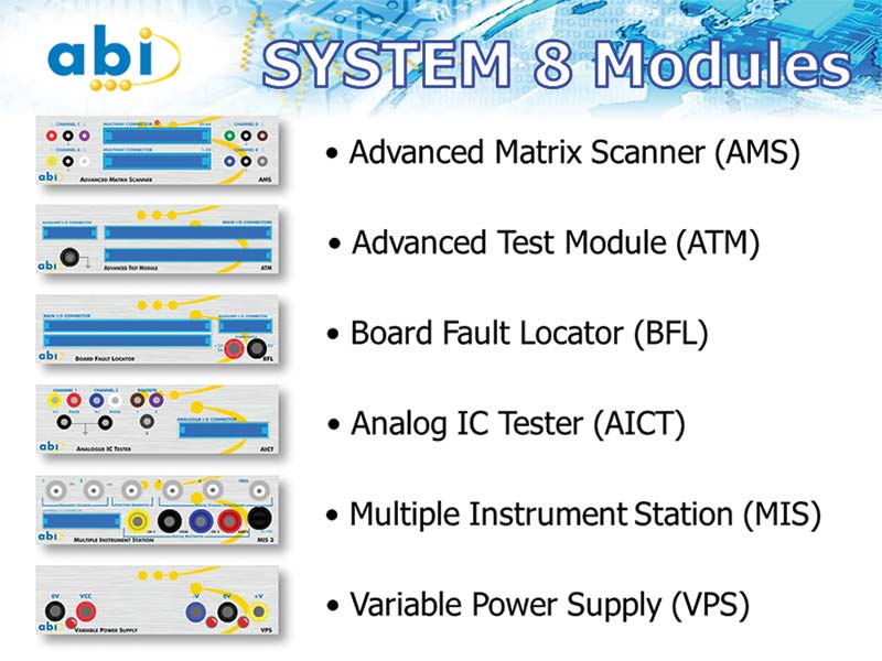
The System 8 software can be configured to guide less well-trained users step-by-step through a test procedure, with custom-annotated picture images, instructions, and attached datasheets to give quick Pass/Fail results. This is much faster and more economical than using traditional oscilloscopes, meters, and other bench test methods. System 8 modules include:
- Board Fault Locator: 64 test channels for multiple test methods for fault diagnosis and functional testing of digital ICs (in-circuit/out-of-circuit), IC connections status, and voltage acquisition, plus V-I curve testing of components on unpowered boards.
- Analog IC Tester: For in-circuit functional testing of analog ICs and discrete components (no programming or circuit is needed). There’s a fully configurable V-I tester for detection of faults on unpowered boards.
- Multiple Instrument Station: Includes eight high specification test and measurement instruments in one module (frequency counter, digital storage oscilloscope, function generator, digital floating multimeter, auxiliary PSU, and universal I/O).
- Advanced Test Module: Offers powerful test combinations for flexible, comprehensive fault diagnosis, including functional, connections, voltage, thermal, and V-I signature tests.
- Advanced Matrix Scanner: 64 channels for fast data acquisition to test high pin count devices as well as complete PCBs; sweep signal frequency to observe DUT response over a frequency range.
- Triple Output Variable Power Supply: Provides required supply voltages to the unit under test.
ATE applications include: PCB testing and troubleshooting, digital/analog IC test, digital/analog V-I test, visual short identification with audible/visual indication of probe distance to short, live board comparison, manufacturing defects analysis, power-on/power-off testing, QA reporting, embedded real time control, calculation and logging, component and board testing, digital and analog functional tests, automated test sequences, etc.
Power Off V/I Testing
If a board can’t be powered up safely, then power-off testing such as V/I and Signature testing can be performed. V/I testing (also known as Analog Signature Analysis) is a technique which is excellent for fault finding on PCBs, and is ideal when diagrams and documentation are minimal. Analog signature analysis can be done with instruments such as ABI Electronics’ System 8 ATM Advanced Test Module (refer again to Figure 5).
This method can be used to perform powered-off troubleshooting of electronic components in printed circuit board assemblies. It could be considered a vital diagnostic tool for PCB repair tasks since it’s suitable for ‘dead’ boards which cannot safely be powered up.
Applying a current-limited AC signal across two points on a circuit causes vertical deflection of the scope trace, while the applied voltage produces a horizontal deflection. This forms a characteristic V/I signature that can show if a component is good, bad, or marginal.
In order to employ the V-I tester to its full potential as a fault diagnosis tool, it’s important to focus on differences between curves for good and suspect boards, rather than analyzing in great detail the meaning of the curves.
The majority of nodes on a PCB will contain parallel and series combinations of components, making exact analysis difficult. The majority of faults on failed boards are major failures such as short or open circuits, which are easy to detect with the V-I technique without complex analysis.
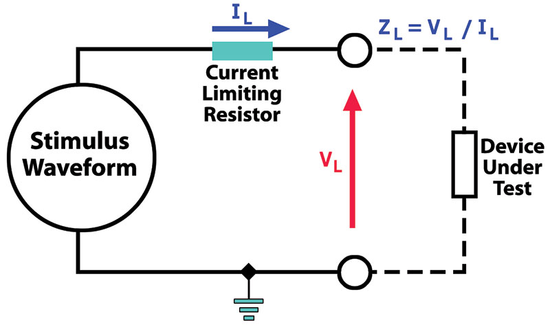
The voltage across the DUT is plotted on the horizontal axis against the current through it on the vertical axis. The stimulus waveform is usually a sine wave. From Ohm’s Law (Z = V/I), the resulting characteristic represents the impedance of the DUT. For frequency-dependent components such as capacitors and inductors, the impedance is frequency related, so a variable frequency stimulus is required.
Most applications use comparative analog V-I testing, so understanding the displayed characteristic is not necessary. The comparison of the curves for a known good board and a suspect board can often identify faults with a minimum of knowledge. Different devices in different configurations produce different signatures, depending on the current flow through the device as the applied voltage changes.
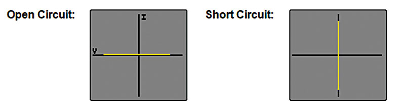
A short circuit, for example, would be displayed as a vertical line because the current flow for any applied voltage would be theoretically infinite (see below), whereas an open circuit would display a horizontal line because the current is always zero irrespective of the applied voltage (see below).
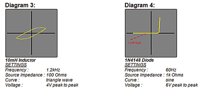
A pure resistor would give a diagonal line whose slope is proportional to the resistance because the current is proportional to the applied voltage. More complex curves are obtained with frequency-dependent components such as capacitors and inductors, and also for non-linear devices such as diode and transistor junctions.
The signatures of resistors are straight lines. The value of the resistor under test affects the slope of the line; the higher the value, the closer the line gets to the horizontal (open circuit). The source impedance of the V-I tester should be selected so the slope of the line (for a good resistor) is as close as possible to 45 degrees. A difference in the slope of the curve when comparing a good and suspect board would indicate a difference in the resistor values on the two boards.
Capacitors with relatively low values have flattened, horizontal, elliptical signatures, and capacitors with relatively high values have flattened, vertical, elliptical signatures. The optimal signature is a nearly perfect circle (see Diagram 2) which can be obtained by selecting the appropriate test frequency and source impedance.
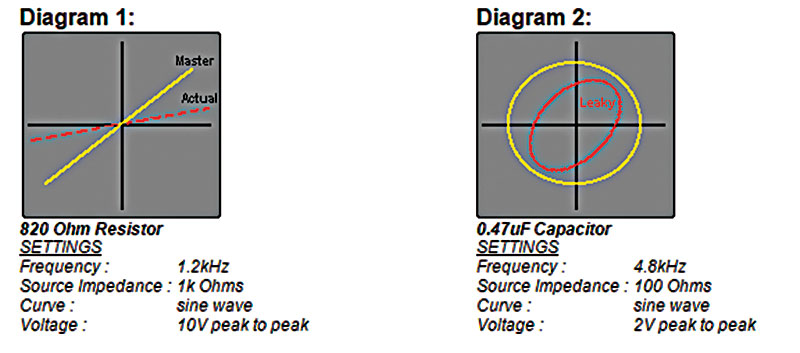
Typically, the higher the capacitance, the lower the test impedance and frequency. A leaky capacitor would give a sloping curve due to the effective resistance in parallel with the capacitor.
Summary
The choice of troubleshooting method depends on the complexity of the circuit and the knowledge and experience of the person who performs the troubleshooting. The methodical use of relevant test tools helps investigators to identify the cause of failure quickly and accurately, and thereby speed up PCB repair.
Businesses realizing the economies of repair versus replace have started incorporating ATEs into their support infrastructure, to their financial and operational advantage. NV