This project started out as a challenge to myself: Could I cram a full-featured Z80 microcomputer using DIP packages onto an ExpressPCB MiniBoard (3.8” by 2.5”)? I have several matched sets of Z80 CPU and peripheral chips that I scavenged from 1980s-era circuit boards that have waited a long time to find a new use. I thought the challenge was impossible, so I approached it as purely a circuit board routing exercise, but then “mission creep” set in. I found that it was possible to fit everything I needed on the board, but how should I set up the I/O addresses, the memory map, or the counter-timer channels?
Soon, I was waist-deep in the Zilog’s Z80 User’s Manual and Z80 Peripherals Manual, learning about interrupt protocols and configuration registers. Before long, I had a schematic that made good use of the available resources in these chips, and it was too good to just write off as a paperwork exercise.
However, the last step of mission creep was the biggest: writing actual code to make it all work. I dislike C syntax, and I didn’t want to use BASIC or any of the other compilers I found out there. So, I gritted my teeth and taught myself Z80 assembly language. Figures 1-3 show the end results.
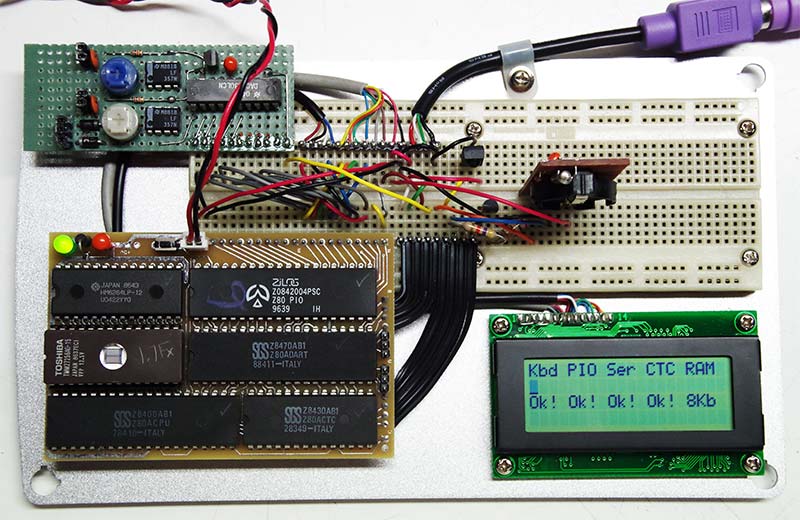
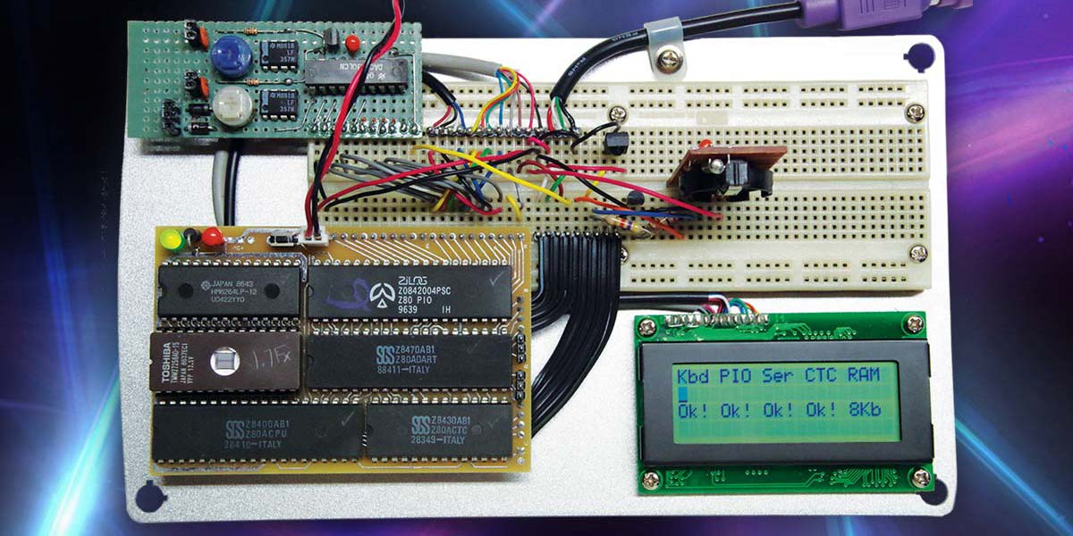
FIGURE 1. Prototype microcomputer board with breadboard testbed, D-to-A daughterboard and 4x20 LCD. Note 1980s date codes!
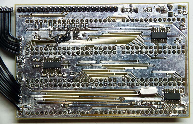
FIGURE 2. Bottom view of prototype board, showing clock crystal and surface mount components. “Dead bug” chip provides startup delay function that I forgot.
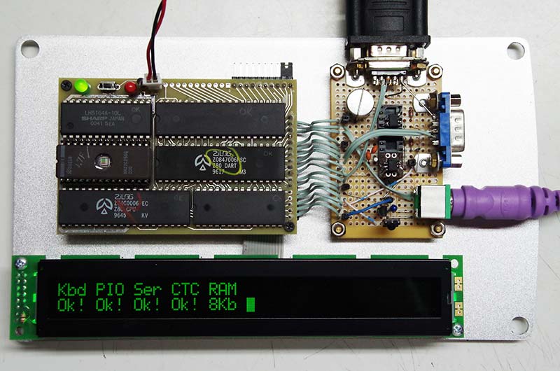
FIGURE 3. Production microcomputer board with expansion/breakout board and 2x40 LCD displaying power-on self-test results.
System Design Goals
Federico Faggin and his team at Zilog put a lot of thought into the design of the Z80 and its peripherals back in the 1970s and I felt obligated to use all the features they included. Most of the existing Z80 system designs I found on the Web were pretty minimal and weren’t a good starting point.
This design includes full use of the Mode 2 interrupt structure, the built-in I/O address decoding abilities, the WAIT function for block data transfers, and all the I/O features of the peripheral chips. I also wanted to add more modern devices to the system such as a PS/2 keyboard and an I2C bus.
Finally, I wanted to keep the system memory simple, both to make the code more straightforward and to minimize parts count. This meant a memory map split into equal halves, no paged memory, and no direct memory access (I didn’t have any DMA chips on hand anyway).
The full schematic is way too detailed to print here (though it and all the other supporting files are available in the article downloads), but Figure 4 shows a simplified block diagram of the core system, and a narrative description of all the circuit connections is available in the online resources.
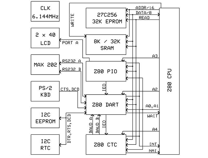
FIGURE 4. Simplified block diagram of the microcomputer.
CPU and Memory
The Z80 has a 64 KByte memory space, which I divided into a 32 KByte EPROM starting at 0000H, and either 8 KBytes or 32 KBytes of static RAM starting at 8000H. Address bit A15 toggles the chip enables of the EPROM and SRAM with the help of an inverter, and a couple of OR gates decode the Read, Write, and MREQ signals from the CPU for the memory chips. A couple of inverters form the system clock, and a couple more form a simple startup delay circuit for the Reset signal.
I took this last function for granted initially, since I’m used to working with microcontrollers that have this delay circuit built in, and wasted a lot of time finding out that the CPU and peripheral chips will start at different times and get out of sync if you don’t have one!
As you’ve already noted from Figure 2, the few logic “glue” chips required for this circuit are surface-mount devices on the bottom of the board, leaving the top of the board populated with the DIP packages for a retro look. The CPU clock speed of 6.144 MHz (for chips rated at 6 MHz) was selected because it divides down nicely to provide standard baud rates for RS-232 communications.
Addressing the peripheral I/O chips is a snap and doesn’t require any external logic. Address lines A0 and A1 are common to all the peripheral chips to select their various control and data registers. Address lines A2 through A7 function as individual active-low chip select outputs for the peripheral chips. The Z80’s IORQ output tells the I/O chips when to interpret these address signals as commands rather than memory addresses. All you need to do is decide how your I/O map is organized, and then specify the proper address byte in your IN and OUT instructions.
The Z80 is the opposite of an RISC (reduced instruction set) processor. It has 158 different instruction types, and I’ve seen it claimed that all possible eight-bit bytes are valid instructions or instruction prefixes (I didn’t count them to make sure). It’s a lot to learn but I really enjoy using their flexibility.
The Z80 also has a large collection of registers to use, including an alternate register set that can be accessed with a single exchange instruction. These alternate registers are handy for servicing interrupt requests without having to PUSH and POP all your main register contents. Although not discussed in the official Z80 User’s Manual, the 16-bit index registers IX and IY can be used as four individual eight-bit registers: IXH, IXL, IYH, and IYL.
Parallel I/O Chip
The PIO chip provides two eight-bit bidirectional I/O ports to interface with “real world” devices like keyboards, disk drives, display controllers, etc. Two handshake pins are provided for each port to latch data to or from these devices. These pins can even generate their own latch signal for each byte sent to an external device that doesn’t have a handshake capability. I use this function to send data to the LCD using Port A.
Port A is also used to send data to a digital-to-analog converter (DAC), using one of the DART outputs as a latch signal instead of the PIO’s handshake pins. Each port can also be configured as a mix of inputs and outputs and can provide interrupts for various conditions. Port B has a (relatively) high current drive capability intended for Darlington power transistors.
DART Serial Communications Chip
This chip is way more than just a two-channel RS-232 Universal Asynchronous Receiver/Transmitter (UART). If you aren’t using the DTR, RTS, CTS, DCD, and RI inputs and outputs to actually coordinate data transfers with an RS-232 device (and who does anymore?), these active-low inputs and outputs can be used as individual digital I/O pins.
The code to read these inputs or toggle the outputs can be a bit lengthy, and there’s a minor caveat in the behavior of the RTS output, but it’s worth it to gain an extra four output and six input pins to use.
There are several interrupts available for serial data transmitting and receiving, plus additional interrupts on the CTS, DCD, and RI “external status” inputs. If you do enable the external status interrupt for one or both of the DART channels, make sure none of these inputs are floating.
In this project, two of these inputs serve the PS/2 keyboard clock and data lines, one serves the I2C data input, and one serves an infrared data receiver module. Because these are digital inputs only and not bidirectional, you can’t send commands to the PS/2 keyboard to turn on the caps lock light, set the typematic rate, etc.
I decided this was a minor issue that didn’t warrant tying up some of the PIO’s bidirectional pins, since I wanted both of its eight-bit ports available for parallel data transfer. I had to get a bit creative using these unidirectional DART inputs and outputs to support bidirectional I2C data flow — more on this later.
The WAIT outputs from the DART chip are designed to connect directly to the WAIT input on the Z80, so that block data transfers to the serial ports don’t need to use interrupts, poll the DART status bits, or rely on fixed delay loops. This simplifies the code quite a bit, though it means the Z80 can’t do other tasks between bytes in the block transfer. If you need the Z80 to work on other tasks between bytes, a simple interrupt handler to manage the block transfer is all it takes.
You can substitute a Serial Input/Output Mark 0 chip for the DART. The SIO/0 is pin-compatible with the DART except that it has bidirectional SYNC pins in place of the DART’s input-only RI pins. It will do everything the DART can do, and also supports several synchronous serial modes. The SIO/1 and SIO/2 chips have slightly different pinouts that omit an I/O pin, so they can’t substitute for the DART.
Counter-Timer Controller Chip
It’s easy to dismiss the CTC as simply a baud rate generator for the DART chip, and it’s (almost) always used for that purpose. The CTC has four independent channels and at most you would use two as RS-232 baud rate generators, so what can we do with the other two channels?
This project uses one of them to provide a watchdog timer — another of those functions taken for granted in a microcontroller but not always found in a microprocessor. One of the baud rate generator frequencies gets divided further in the third CTC channel, and the output (I chose 10 Hz) is fed to the Z80’s non-maskable interrupt input. [Note that this arrangement lets you “mask” the non-maskable interrupt and disable the watchdog timer temporarily by stopping the baud rate generator that drives the third CTC channel input.]
The NMI interrupt handler must start at code address 0066H and can check for whatever code execution status conditions need to be monitored. The NMI handler automatically disables maskable interrupts during its execution and re-enables them with a RETN instruction on return to normal program flow. In my example code, I use the CTC’s watchdog timer interrupts to provide an up-timer. The fourth CTC channel (which lacks an output pin) is used as a general-purpose external event counter.
Interrupts
The Z80 has several big improvements over the earlier 8080 microprocessors. One of the biggest is in interrupt handling. Mode 2 interrupt handling is the most powerful Z80 option and allows the requesting device to provide the interrupt service vector to the Z80. The CPU doesn’t have to poll any peripheral status bits to find out what condition generated the interrupt; it can simply jump to the relevant handler.
Mode 2 supports prioritized interrupts and nested interrupts (i.e., when a higher-priority interrupt interrupts a lower-priority interrupt service routine already in progress).
To use Mode 2, you need to establish an interrupt vector table in memory (usually in the code, but it can be in RAM if you need to modify it dynamically), and you need to write the interrupt handling routines that these vectors point to. Then, load the appropriate interrupt vector into each I/O chip, enable the interrupts that you intend to use, and set the “status affects vector” bit in the DART so that each of its interrupt-generating conditions will send a unique vector.
I/O chip interrupts are “daisy-chained” using their IEI and IEO pins to establish their priority. They’re also daisy-chained internally because each chip contains more than one interrupt-generating device, and their internal device priorities are fixed. There are two in the PIO, four in the CTC, and six in the DART.
This is important because when an interrupting device signals the Z80, it also disables interrupts in all lower-priority devices, and this “disable” signal will only propagate through eight devices (not chips) before the Z80 starts handling the interrupt request.
In this design, the PIO has the highest interrupt priority, followed by the DART, and then the CTC. “But wait!” you say, “The PIO and DART use up all eight daisy-chain devices, so how can the CTC interrupts be used?” The answer is the disable signal propagation doesn’t always start at the first daisy-chained device. For example, if you disable the PIO interrupts, then the six DART device interrupts and the first two CTC device interrupts can be used together.
This may be more than you wanted to know about Z80 interrupts, but they are so powerful and such a defining feature of a “real” microcomputer system that I wanted to highlight them. They’re also one of the few features that I found easier to understand and code in assembly language than in a high-level language.
I2C Interface
If you read the official Philips I2C specifications carefully, you’ll find that for the vast majority of I2C applications (i.e., single master, no clock stretching by peripheral devices), the I2C clock signal can be a unidirectional output from the master to the peripherals. The data signal must be bidirectional and as with the PS/2 keyboard inputs, I didn’t want to waste a bidirectional PIO pin if I could help it.
Figure 5 shows a simple interface circuit that turns two outputs and one input on the DART into the two standard I2C bus connections.
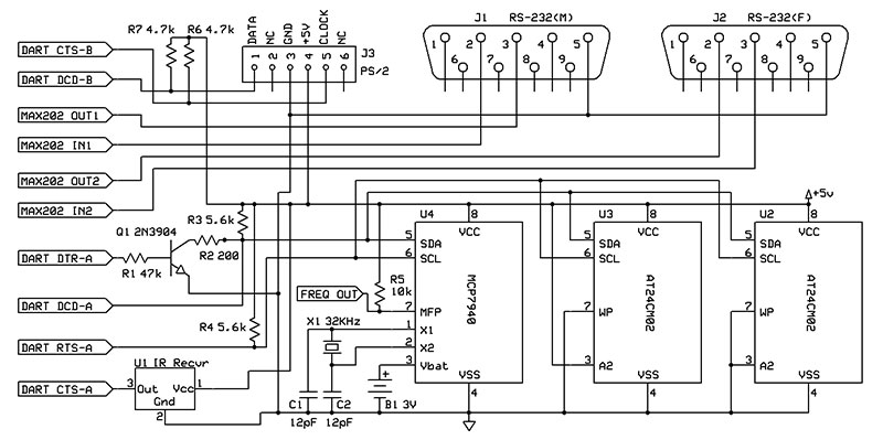
FIGURE 5. Schematic of the expansion/breakout board. The I2C interface uses the DART’s DTR-A and RTS-A outputs and DCD-A input.
The expansion/breakout board shown in Figure 3 includes this interface circuit and has sockets for three I2C chips. I’ve populated them with two AT24CM02 256 KByte EEPROMs and an MCP7940 real time clock and calendar with battery-backed SRAM. I see the EEPROMs as the rough equivalent of period-appropriate eight inch floppy disk drives, while the MCP7940 stands in for the old MC146818 real time clock chip.
Coding and Assembling
Z80 opcodes and their mnemonic structures are pretty straightforward and consistent, though there are quite a lot of them. The monitor program code I’ve written (in the downloads) is more of a demo and function library, so use it to get the feel for the code structure and then pick and choose from these subroutines to build your own application.
Turning PS/2 keyboard codes into ASCII characters, sending data to an LCD display, reading and writing blocks of data via I2C, converting ASCII to HEX to decimal, decoding Sony SIRCS infrared codes, interrupt service routines, peripheral chip configuration bytes, direct digital synthesis using an external DAC, a power-on self-test routine, and more are included.
Rather than using this microcomputer to run a simple BASIC interpreter as I’ve seen in other designs, try your hand at building a file system for the EEPROMs, a bootloader, a command-line interpreter, or even a bare-bones operating system. I’m not that familiar with the old CP/M operating system, but you might be able to port it to this microcomputer design.
There are a lot of Z80 resources available online (see Resources). The most important ones are the Zilog user’s manuals for the Z80 and the peripheral chips. A word of warning, though. The Z80 User’s Manual, and to a lesser extent the Z80 Peripherals Manual, contain a bunch of typos and errors. Many are due to bad optical character recognition, some are copy and paste errors, and a few are even funny. I was always able to figure out what the correct information was from context, but sometimes it took some doing.
I use the freeware assembler Zeus to generate the HEX files to burn to the EPROM. It’s very easy to use, comes with a bunch of example files, includes an emulator, and handles the “unofficial” Z80 instructions such as those that use the upper and lower bytes of the IX and IY index registers separately.
Look for the assembler directives at the beginning and end of my code that define the format of the output HEX file. In case you don’t have your own EPROM programmer, the online resources include a schematic and code for a very simple one I designed based on a PIC16F887 microcontroller (Figure 6) that accepts raw HEX data via a RS-232 serial link.
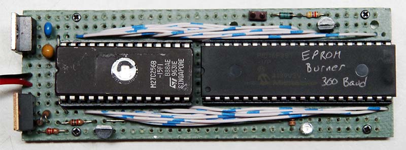
FIGURE 6. Homebrew PIC-based EPROM programmer with RS-232 interface.
Challenge Accepted!
I put a fair amount of effort into the layout of the surface-mount parts on the bottom of this board to make them easier to solder by hand (wider trace widths, ample spacing between adjacent parts, and relatively “large” 0805 and SOIC parts), but if you aren’t confident of your soldering skills, you can build the project using all through-hole parts too. However, you might have to add buffer chips on the address and/or data buses if your layout ends up sprawling over an entire S-100 bus board and the bus capacitance gets too high for the Z80 to drive reliably.
There are pads for optional 10K ohm pull-up resistors for the PIO Channel B pins in case you want to use them as inputs. Space constraints forced me to place the clock oscillator crystal on the bottom of the board, so make sure to put an insulator under this component when you install it, and make sure you install it before you install the microprocessor. Also, make sure to put a solder bridge on the appropriate SRAM size select pads before installing the SRAM chip.
If you end up buying new Z80 and peripheral chips rather than using parts scavenged from older machines, they may be rated at 10 MHz or above. In this case, I recommend increasing the system clock speed to 9.8304 MHz to use those chip’s full capabilities. Otherwise, you can use a 2.4576, 3.6864, or 6.144 MHz crystal depending on whether you’re using Z80, Z80A, or Z80B series chips. These clock speeds all divide down nicely to standard RS-232 baud rates, though you will have to recalculate the time constants for the CTC chip.
EPROMs and SRAMs rated at 200 ns access time are more than adequate for a clock speed of 6.144 MHz since the CPU takes two clock cycles to complete an instruction opcode fetch and three for a memory read or write. I recommend using EPROMs and SRAMs with a 150 ns access time or better for a 9.8304 MHz clock.
Don’t feel that you need to copy the expansion/breakout board design I used since not everyone will want to use the same peripherals I’m using or use the same I/O pins to connect to them. However, all of the connections are described narratively in the supporting documents online, and my code includes loads of comments on the code itself and the hardware connections the various subroutines are designed for.
At this point (or maybe several pages back), you may be wondering why anyone would put this kind of effort into a computer architecture that has its roots back in the 1970s. To me, it’s a matter of historical perspective. It’s true that modern microcontrollers can do everything this microcomputer design can do and more in a much smaller footprint. But it’s also true that this microcomputer design is more compact and capable than 1970s and early 1980s personal computer systems.
This architecture is relevant even today. Z80 chips are still being manufactured and used in a variety of applications more than 40 years after their introduction. So, take the Z80 challenge and build something that’s both classic and modern at the same time. NV
Parts List
| Parts List |
Mouser Part No. |
| Z80 CPU, 40-DIP, 10 MHz |
692-Z84C0010PEG |
| Z80 PIO, 40-DIP, 10 MHz |
692-Z84C2010PEG |
|
Z80 DART, 40-DIP, 6 MHz
or Z80 SIO/0, 40-DIP, 10 MHz
|
692-Z0847006PSG
692-Z84C4010PEG]
|
| Z80 CTC, 28-DIP, 10 MHz |
692-Z84C3010PEG |
| 27C256 32KB EPROM, 28-CERDIP |
eBay |
| 62256 32KB SRAM, 28-DIP, 0.6” |
913-AS6C62256A-70PCN |
| MAX202 RS-232 Transceiver, 16-SOIC |
700-MAX202CSE |
| 74HC04 HEX Inverter, 14-SOIC |
757-74HC04DBJ |
| 74HC32 Quad OR Gate, 14-SOIC |
757-74HC32DBJ |
| 74AHC1G08 AND Gate, SOT-23-5 |
595-SN74AHC1G08DBV3 |
| (10) 0.1 µF Ceramic Capacitors, 0805 |
710-885012207098 |
| (2) 30 pF Ceramic Capacitors, 0805 |
80-C0805C300J5G |
| 10 µF Tantalum Capacitor |
581-TAP106K020GSB |
| (2) 1K ohm Resistors, 0805 |
603-RT0805FRE071KL |
| (4) 10K ohm Resistors, 0805 |
603-RT0805FRE0710KL |
| 100K ohm Resistor, 0805 |
603-RT0805FRE07100KL |
| 1M ohm Resistor, 0805 |
603-RT0805FRD071ML |
| SR220 Diode, 2A 200V |
821-SR220R0G |
| T-1 3/4 Green LED |
78-TLHG6400-CS12Z |
| SPST Momentary Switch |
611-PTS635SH50LFS |
| 28-DIP Socket, 0.6” |
649-DILB28P223TLF |
| 6.144 MHz Crystal, HC-49US (see text) |
744-ATS061 |
Resources
www.z80.info
Tons of datasheets, designs, code examples, and links to other resources.
www.desdes.com/products/oldfiles/zeus.htm
Zeus assembler for Windows PCs.
“Programming the Z80”
by Rodnay Zaks. SYBEX, 1980. ISBN: 0-89588-094-6.
Downloads
What’s in the zip?
PCB Files
Schematic Files
Text Files
Circuit Description