The compound pair has two transistors of opposite polarity (NPN, PNP) connected together to give the maximum current and power gain possible. The arrangement is different to the Darlington pair, so, for example, circuits using positive feedback become possible. You can construct a wide range of projects using this simple combination from audio amplifiers to light sensors to pulse generators, often having the merit of a low component count. The compound pair highlights many interesting technical aspects of transistor behavior, especially as the first transistor operates in the common emitter mode at a very low current.
The Basics
The basic motif is shown in Figure 1.
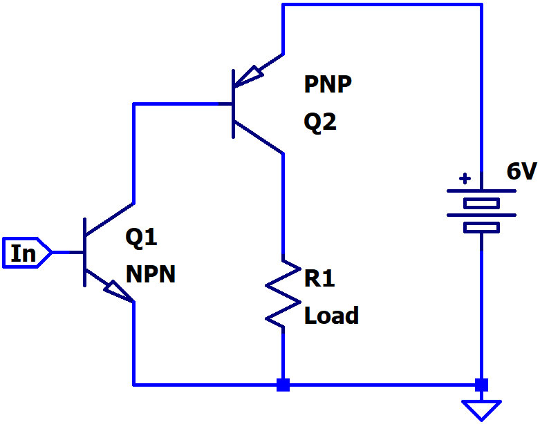
Figure 1. A compound NPN, PNP transistor pair. A small current flowing through the base emitter junction of Q1 becomes a large current flowing through the load resistance R1.
Q1 is in a common emitter arrangement. A small current flowing through the base emitter junction of Q1 causes a larger current to flow through its collector, which then flows through the base emitter junction of Q2 (also in common emitter mode). This results in even greater current gain.
The result is two rounds of current amplification; first by the hFE (current gain) of Q1, and secondly by the hFE of Q2. For typical values of hFE of around 300, the total current gain is quite impressive at 90,000 (300*300).
You can also swap around the polarity of the transistors as in Figure 2.
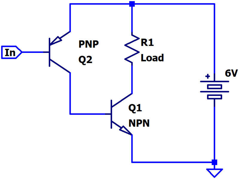
Figure 2. A PNP, NPN compound pair. Connecting a large value resistor from In to ground will result in a large current flowing through the load resistor R1.
This can be helpful when using NPN power transistors from scrap compact fluorescent lamps that on their own have too low an hFE to be useful.
The most common application of the compound pair is as a replacement for the Darlington pair.
In that mode, it’s often called the Sziklai pair and is shown in Figure 3.
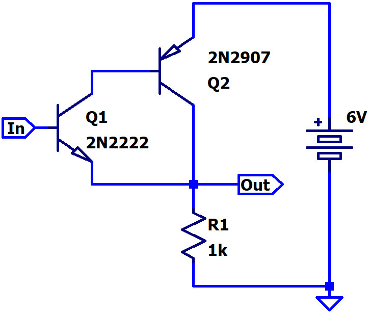
Figure 3. The Sziklai pair. A voltage present at In is copied to Out minus about 0.7 volts. The current required at In is tiny; the current available at Out is much larger.
It’s commonly used in high power class B audio amplifiers. It has a smaller voltage drop (0.7 volts) than the Darlington pair (1.4 volts).
Current Gain
As an example of the great current magnification of the compound pair, you can contemplate the use of an LED as a photocell. Since the semiconductor junction area is minute, the current generated when an LED is illuminated is tiny. Actually, it’s so small it’s difficult to read with a regular multimeter. You would almost think the effect didn’t exist.
Using the circuit in Figure 4, you can see that some current is genuinely produced.
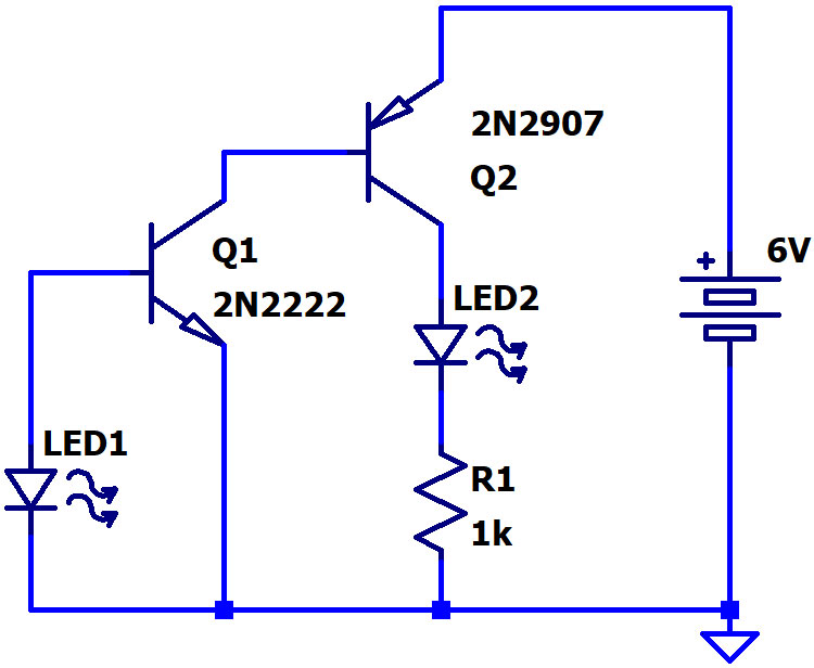
Figure 4. An LED as a photocell. Illuminating LED1 causes LED2 to illuminate.
Voltage Gain and Biasing
Does the high current gain available from the compound pair translate to high signal voltage gain? There is a slight problem due to the very high input impedance of the first transistor, which follows from the fact that it’s operating at a very low current.
A high input impedance means you have to vary the input voltage a lot for the input current to vary a little. In the audio preamplifier circuit in Figure 5, R5 is added to increase the current flowing through Q1.
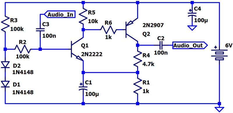
Figure 5. An audio preamplifier with high signal voltage gain.
This increases the gain from 100 if R5 was omitted to a more respectable 700 or so.
To bias the circuit, it’s necessary to make use of voltage follower behavior. The diodes D1 and D2 in series provide 1.4 volts into the base of Q1. That results in 0.7 volts appearing at the emitter of Q1.
However, most of the current to cause 0.7 volts to appear across R1 is actually provided by Q2 through R4. The voltage across R4 then is 4.7*0.7 = 3.29 volts approximately which correctly biases the circuit.
C1 prevents negative feedback from drastically reducing the gain of the circuit. It filters audio signals to ground. R6 is needed to prevent C1 from being charged rapidly at switch-on through Q1 and the base emitter junction of Q2. The high charging current might otherwise damage the two transistors.
Another way to bias the compound pair is using a current mirror as in Figure 6.
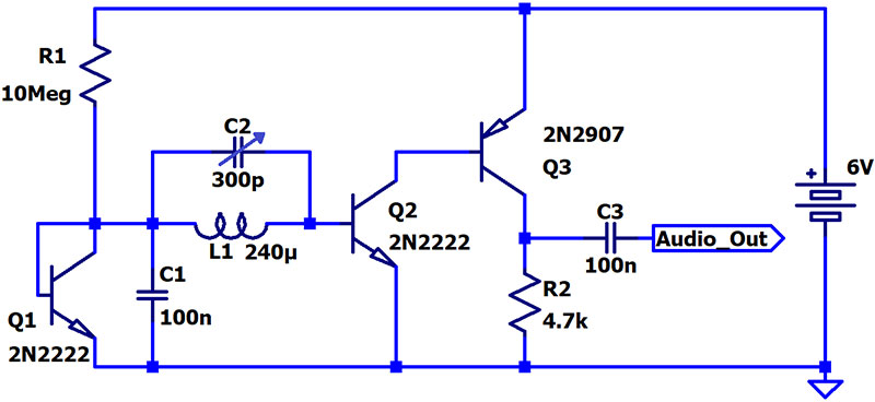
Figure 6. A tuned radio frequency (TRF) receiver. You can use a ferrite rod antenna for L1.
At DC, the inductor L1 is basically a straight through connection, meaning that Q1 and Q2 form a current mirror. The voltage across R1 is approximately 6 - 0.6 = 5.4 volts. The current then is 540 nA.
If Q1 and Q2 are matched, then the current at the collector of Q2 is also 540 nA. This current is then multiplied by the hFE of Q3 which might be around 300. That would give a current of 0.16 mA at the collector of Q3.
Of course, the biasing is not certain using such a scheme, and some adjustment of R1 may be necessary.
The high input impedance of Q2 avoids damping the tuned resonant circuit L1 and C2, allowing such selectivity as the Q of the tuned circuit provides. AM detection is by the non-linear behavior of Q2 to voltage signals.
The current at the collector of Q2 is so low that the frequency response is limited by stray capacitance and the radio frequency component is effectively filtered out, leaving Q3 to amplify the remaining audio component.
Positive Feedback
Since the output of the compound pair increases when the input increases, there exists the possibility of using positive feedback. The simplest example is the Schmitt trigger shown in Figure 7.
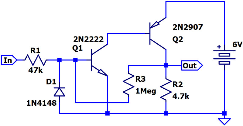
Figure 7. A Schmitt trigger with wide input voltage tolerance.
When the voltage at In exceeds a threshold of about 0.6 volts, Q1 starts to conduct; Q2 even more so. The voltage across R2 increases and is feedback to the input via R3. This causes Q1 to conduct even more strongly, resulting in a snap on.
To reverse the process, you have to reduce the voltage at In by about 0.2 volts, which causes the system to snap off. The circuit is tolerant to wide swings of input voltage because R1 is quite large in value. D1 prevents a reverse base emitter junction breakdown of Q1 when the input voltage is very negative.
Another application of positive feedback is to create a pulse oscillator as shown in Figure 8.
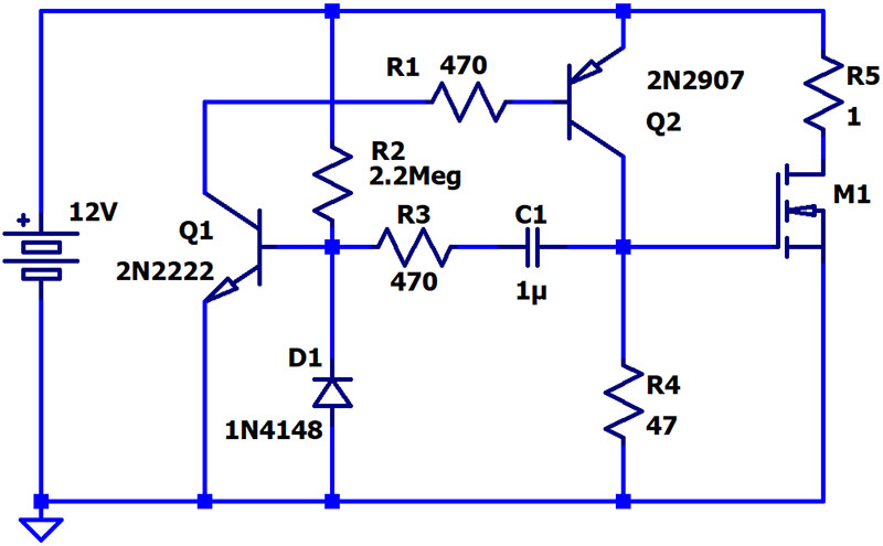
Figure 8. A pulse oscillator circuit.
R2 slowly causes C1 to charge until Q1 starts to conduct. Q2 snaps on and forces current through C1 and R3 into the base of Q1. When C1 has fully charged, there’s a sufficient drop in voltage at the collector of Q2 to drive the system the other way. Q1 and Q2 snap off.
The load resistor R4 has to be relatively low in value for the system to work. The output is ideal for driving a MOSFET if you want even more powerful current pulses.
In the example, there are 12 amp pulses going through R5. The MOSFET M1 can be any suitable type that can handle high current. R1, R3, and D1 are present to prevent damage to the transistors from excess currents and reverse voltages.
At lower voltages and when powering the circuit from high internal resistance zinc carbon batteries, you can omit them. C1 should really be a ceramic or film capacitor.
The circuit can be adapted in many ways to construct high voltage generators, DC-to-DC converters, LED drivers, and as a high harmonic content signal generator to test audio and radio circuits.
I hope you find you’ve found this article helpful and do some experimenting on your own. NV