Twenty plus years ago, I published an article in Nuts & Volts about designing a general-purpose programming system. Back then, I had collected over a dozen programmers for use with different chips. I thought about purchasing an expensive “universal” programmer but ultimately decided to design my own: the LP120. The LP120 provided the basics needed in any programmer while the programming module (that plugs into an edge connector) provides additional circuitry that may be unique to the particular chip being programmed.
I’ve used the LP120 heavily for the last 20 years to support my eight-bit design hobby. It now has uploadable drivers and programming modules for many eight-bit micros (Motorola and PIC), EPROMs, and GALs. However, things have changed since 2000. Back then, few microcontrollers had more than 4K bytes of program memory and now eight-bit PICs have up to 64K of memory.
Clearly an update to the LP120 was called for.
DESIGN GOALS
Of course, I wanted to make the transition to my new LP130 as easy as possible, not only for myself, but for the several Nuts & Volts readers who I know built LP120s. When I decided to update the LP120 and create the LP130, I set several goals for the LP130:
- The LP130 should be able to use all the programming modules developed for the LP120 while adding a high-speed serial link for programming modules.
- To the maximum extent possible, the processor used in the LP130 should be software compatible with the MC6803 used in the LP120.
- The LP130 should run faster than the LP120.
- Maintain the RS-232 serial link used by the LP120 and add a more modern serial link.
- Increase the memory available to buffer program data.
- Maintain the same footprint as the LP120.
- Maintain the same power supply requirements as the LP120.
I was able to achieve all the design goals:
- The LP130 uses the same edge connector as the LP120. All the connections are the same except for three which were not used by any LP120 programming module and are now used for an SPI link between the LP130 processor and the programming module. With SPI, future programming modules can store driver programs in onboard serial EEPROMs.
- The LP130 uses an MC68HC11 processor which is source and object code compatible with the MC6803. Development applications for the MC6803 are not well supported under recent versions of Windows, so writing drivers for the LP120 has become difficult. The MC68HC11 is well supported by Windows applications. The source code for LP120 drivers can be modified relatively easily by substituting the MC68HC11 register definitions in place of those for the MC6803.
- The LP130 runs at 7.3728 MHz — twice the speed of the LP120.
- The LP130 has a RS-232 serial link that runs in parallel with an optional Bluetooth link. The optional Bluetooth serial link can be added with an HC-06 Bluetooth module. Sometimes I connect from an old computer using a standard RS-232 serial cable and sometimes from my Win10 machine using TeraTerm via a USB-serial adapter or Bluetooth.
- The LP130 maintains the same 40K of parallel RAM used in the LP120 and adds 256K of SPI serial RAM. If Microchip develops denser serial RAM chips in the future, more than 256K is possible. For older micros and GALs, the drivers can continue to use only parallel RAM. For PICs and large EPROMs, the serial RAM will hold the program data while the driver runs out of parallel RAM.
- The LP130 maintains the 6.75 x 5.75 inch footprint. The mounting holes and the programming module edge connector are in the same place as the LP120. This will allow any case someone built for the LP120 to work with the LP130.
- The LP130 has the same power supply requirements: +5 VDC at 750 mA and +15 VDC, or +14 to +16V unregulated at 1A.
Figure 1 shows the block diagram of the LP130 programming system.
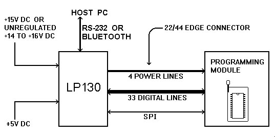
FIGURE 1. LP130 block diagram.
Many of the design features of the LP120 remain unchanged. Programming-pulse voltages can vary from 25V for some of the older EPROMs to 5V for Flash devices. Typically, the tolerance on the programming-pulse voltage is ±0.25V. Therefore, the programming-pulse voltage (VPP) should cover at least 5 to 25 volts with better than 0.25V accuracy.
To fully comply with published programming algorithms, the supply voltage to the part being programmed also needs to vary. For example, some 5V EPROMs are programmed while powered at 6.5V, and PIC microcontrollers are verified at the min and max supply voltages. Typically, the tolerance on supply voltages is ±0.1V. Therefore, the programmer should be able to power the device being programmed with voltages from 3 to 6.5 volts with better than 0.1V accuracy. I use the symbol Vps for this voltage because it’s the voltage supplied to the programming socket.
Including address, data, and control lines, an EPROM may need 26 digital interface lines for proper programming. Therefore, the programmer should provide at least 26 bi-directional digital lines to interface with the device being programmed.
LP130 CIRCUITRY
Microcomputer
The LP130 is an eight-bit microcomputer system with its own RAM, EPROM, and I/O. Figure 2 is the 68HC11 microcomputer (U1), address latch (U2), and clock oscillator (Y1).
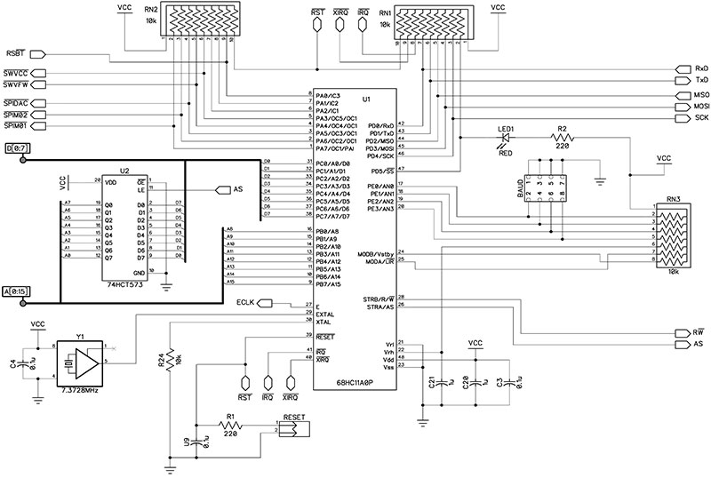
FIGURE 2. LP130 microprocessor schematic.
The 68HC11 provides a 64K byte-wide address space, an asynchronous serial communications interface (Motorola calls this an SCI instead of UART), a synchronous serial peripheral interface (SPI) port, and a parallel port all in one chip.
The E-clock output of the 68HC11 (pin 27) is a square wave at one-fourth the crystal frequency or 1.8432 MHz. Figure 1 also shows the pin selectable BAUD rate header and the RESET header.
Memory
Figure 3 shows the parallel memory in the 68HC11’s memory space.
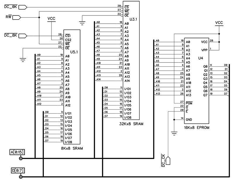
FIGURE 3. LP130 parallel memory schematic.
The LP130’s firmware is stored in a 27128 EPROM (U4). The 62256 and 6264 chips (U3 and U5, respectively) form 40K of continuous RAM.
The firmware doesn’t have the code to program all the devices the LP120 is capable of programming; it only contains the operating system, test routines, and hooks to lots of subroutines.
To program a specific device, “driver” software must be uploaded to the LP130 and executed out of RAM. In the last 20 years, the footprint of RAM chips has changed so the LP130 circuit board was laid out to accept either 300 or 600 mil wide DIP packages for the 62256 and 6264 chips.
SPI Peripherals
Figure 4 shows the SPI peripherals connected to the 68HC11. U10 and U11 are both 23LC1024, 128K x 8 serial RAM chips. The MCP4802 (U12) is a dual eight-bit voltage output SPI/digital-to-analog converter (DAC). This dual DAC provides the reference voltages for the Vpp and Vps power supplies.
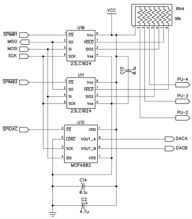
FIGURE 4. LP130 serial memory and digital-to-analog converter.
Serial Communications & Baud Rate
The serial communications schematic is shown in Figure 5.
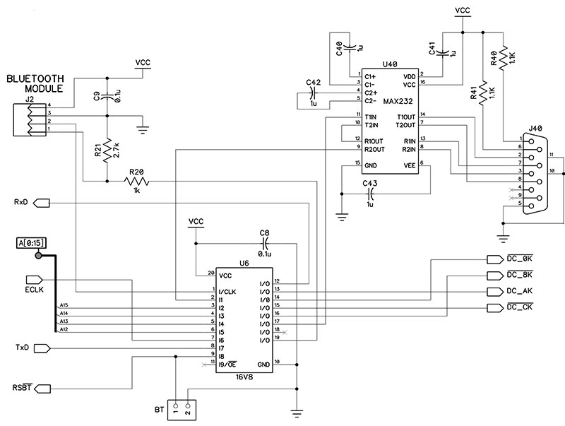
FIGURE 5. LP130 memory decoder and serial communication interface.
The RS-232 serial connector is a female DB-9 type, wired as a DCE device. This mates directly with the nine-pin DTE connectors found on most PCs or USB-serial adapters. The MAX232 (U40) contains two RS-232 drivers, two RS-232 receivers, and an on-chip charge-pump. The charge-pump uses the five volt supply to generate the bipolar voltages needed by the RS-232 drivers. RTS is received, buffered, and looped back to CTS, so CTS tracks RTS. DCD and DSR are both held in the ON condition.
Optionally, Bluetooth serial communications are possible by inserting a HC-06 in header J2 and placing a jumper on the Bluetooth header (BT). The HC-06 is a class 2 slave Bluetooth module designed for transparent wireless serial communication. Once it’s paired to a master Bluetooth device — such as a PC or smartphone — its operation becomes transparent to the user.
When pairing, the LP130 should appear as “LP130” when scanning for connections. All data received on the HC-06’s serial input is immediately transmitted wirelessly. When the HC-06 receives wireless data, it’s sent out through the serial interface exactly as it’s received.
The baud rate is always 9600 when using the Bluetooth connection, BT jumper present. When using the RS-232 connection, BT jumper off, the baud rate can be set by the jumper on the BAUD header. Possible baud rates are 4800, 9600, 19200, and 38400. If there is no jumper on the BAUD header, the baud rate defaults to 9600.
Address Decode
Figure 5 also shows the ATF16V8 generic array logic (GAL) chip used for address decoding. The 62256 (32K byte) RAM decodes from $0000 to $7FFF, the 6264 (8K byte) RAM decodes from $8000 to $9FFF, the peripheral interface adapters (PIAs) decode at $AXXX, and the 27128 (16K byte) EPROM decodes from $C000 to $FFFF.
The GAL also multiplexes the RS-232 and Bluetooth serial data to the 68HC11.
Power Control
Figure 6 shows the power control circuitry. Power connects to the LP130 at J1; VCC (+5V), VFW (+15V), and ground.
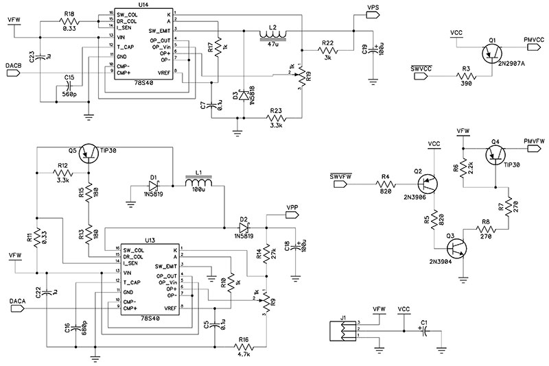
FIGURE 6. LP130 power control circuitry.
Transistor Q1 can switch VCC to the programming module where it’s called PMVCC. Circuitry on the programming module should draw no more than 100 milliamps from PMVCC.
Transistors Q2-Q4 can switch VFW to the programming module where it’s called PMVFW. Circuitry on the programming module should draw no more than 500 milliamps from PMVFW.
The converter circuits for VPP and VPS are both powered by VFW and both are controlled by voltages from the MCP4802 dual eight-bit DAC. The DAC voltages go to the reference inputs (pin 9) of the 78S40 switching voltage regulators (U13 and U14). The 78S40s will change their output voltage to make the feedback voltage (pin 6) equal the reference input (pin 9).
The VPP circuit is the lower part of Figure 5. U13 is configured as a step up/down switching regulator. This configuration allows VPP to be above or below the nominal 15 volts on VFW. The circuit shown allows VPP to be set from 4.5 to 25.5 volts in 0.1V steps.
The VPS circuit is the upper part of Figure 5. U14 is configured as a step-down switching regulator. VPS powers the programming socket and any other circuitry on the programming module that must operate at the same voltage. The circuit shown allows VPS to be set from 1.8 to 7.5 volts in 0.03V steps.
I’ll have an article in the next issue that will cover the 78S40 universal switching regulator and details of the programmable power supplies.
Parallel I/O & Programming Connector
Programming a device like an EPROM requires a large number of digital lines for the address and data lines which must be steady while a byte is programmed. This means the EPROM being programmed can’t be connected to the address or data bus of the 68HC11. Therefore, parallel ports are used to set the address and data for the device being programmed.
Figure 7 shows U7 and U8, the two 68B21 parallel interface adapters (PIAs).
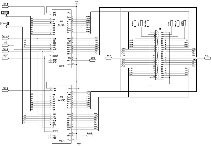
FIGURE 7. LP130 peripheral interface adapters and programming module connector.
The PIA’s four bi-directional parallel ports and one bi-directional control line are all routed to the programming connector.
The programming connector (J3) is an edge connector with 44 contacts (22 per side) at 0.156 inch spacing. In addition to the digital lines from the PIAs, the four switched voltages and the SPI port are routed to the programming connector.
PROGRAMMING MODULES
The programming module for the specific device being programmed plugs into J3. In addition to the device being programmed, the programming module contains any required circuitry not provided by the LP130. This might be glue logic, a transistor-switch controlled by the device being programmed, a level translator, etc.
The device being programmed should be powered by VPS while the programming pulse voltage should be supplied by VPP. Data, control, and address lines on the device being programmed should be connected to the bi-directional parallel ports from the PIAs.
If a particular device doesn’t use all the digital lines or voltages, it’s only connected to those it needs. Programming modules are small and can easily be built using wire-wrap or point-to-point wiring. Many vendors (including Lucid Technologies) sell 44 contact plug-in boards that are perfect for the job.
LP120 FIRMWARE
Opening Menu
Whenever the LP130 is turned on, the firmware operating system will initialize the hardware and send an opening menu like the one shown here to the host. Menu selections are made by typing the character in brackets. Any other character will cause the menu screen to be retransmitted.
LP130 Programmer
Firmware 2021.01.01
(C) Lucid Technologies 1990-2021
-------- LP130 OPENING MENU --------
[U]pload driver program
[J]ump to driver at 0100 hex
[D]isplay system memory
[T]est parallel static RAM
[C]alibrate Vpp and Vps
?
[U]pload Driver Program
This option is used to upload the driver for the device you want to program. Drivers are stored as ASCII files in the Motorola S-record format. The upload is accomplished via the ASCII file transfer facility of whatever terminal/communication program you’re using on the host.
After uploading, control should automatically transfer to the driver program and its menu screen should appear. If the LP120 OPENING MENU reappears, use the [J]ump option to start the driver.
[J]ump to Driver at 0100 Hex
Use this option to transfer control to 0100 hex which is the starting address for driver programs.
[D]isplay System Memory
This option is included as a debugging aid for users who write their own device driver programs. Any portion of the LP120 memory space can be displayed, including the serial RAM.
[T]est Static RAM
This test checks the RAM in the 68HC11’s address space from 0040 to 9FFF. Each memory scan writes a test byte at every address, then goes back and reads every address to confirm the data is correct. The test byte is incremented with each new scan.
An “*” is printed on the screen every 256 scans. If an error is encountered, the test will halt and the address of the bad byte will be displayed. The test may be stopped at any time by pressing the ESCape key.
[C]alibrate VPP and VPS
Use this option to calibrate the DC-to-DC converter circuits. This calibration trims the gain of the DC-DC converters so that their outputs match the voltages called for by the microprocessor.
DEVICE DRIVER PROGRAMS
The device driver is a necessary part of the software for programming any device. The LP130 firmware alone is not capable of programming anything. Device driver programs are transient programs loaded into the LP130’s RAM.
The first step in programming any device is to upload the device driver for that part. The device driver will present its own menu, usually with another upload option for the data to be programmed into the device. Of course, device drivers must verify the programming is correct, so they are able to read programs from chips as well as write programs into chips.
Writing Device Drivers
I’ve written device drivers for 2716-27256 EPROMs, 68705P/R/U/J1A microcontrollers, 6801 and 68701/U4 microcomputers, PIC mid-range microcontrollers, and ATF16V8 GALs. All the device drivers were originally written for the LP120 in 6803 assembly language, then reassembled for the 68HC11. Writing the device drivers isn’t hard and the assembly language Toolbox that comes with the LP130 makes it easier. In my experience, the hardest thing is finding and understanding the programming specifications from the chip manufacturers.
LP130 Firmware Toolbox
Part of the documentation that comes with every LP130 is an assembly language header that contains equates for all the 68HC11 and 6821 registers and firmware Toolbox subroutines. These subroutines provide a programmer’s Toolbox that can handle most of the low-level I/O and data conversion required in any device driver. The complete list of current Toolbox equates is shown in Table 1.
| RESET |
EQU |
$FD80 ;JMP Here to terminate driver, clears RAM. |
| EXITMM |
EQU |
$FD84 ;JMP Here for LP130 Main Menu, RAM intact. |
| ADRBCD |
EQU |
$FD88 ;JSR Return address of BCD data in X. |
| ADRHEX |
EQU |
$FD8C ;JSR Return address of Hex-record data in X. |
| ADRMOT |
EQU |
$FD90 ;JSR Return address of S-record data in X. |
| ADRMSG |
EQU |
$FD94 ;JSR Return address of message buffer in X. |
| ADRSPI |
EQU |
$FD98 ;JSR Return address to 24-bit serial RAM address. |
| ASCHEX |
EQU |
$FD9C ;JSR Convert ASCII character in A to hex. |
| BCD08 |
EQU |
$FDA0 ;JSR Convert B to BCD. |
| BCD16 |
EQU |
$FDA4 ;JSR Convert D to BCD. |
| DLY_A |
EQU |
$FDA8 ;JSR For delay approx. (25 uSEC)*X. |
| DMP16B |
EQU |
$FDAC ;JSR Display 16 bytes as HEX then as ASCII. |
| DMPNB |
EQU |
$FDB0 ;JSR Display N bytes as HEX then as ASCII. |
| DMP8W |
EQU |
$FDB4 ;JSR Display 16 words as HEX then as ASCII. |
| DMPNW |
EQU |
$FDB8 ;JSR Display N words as HEX then as ASCII. |
| DWNHEX |
EQU |
$FDBC ;JSR Download data as a Hex-record. |
| DWNMOT |
EQU |
$FDC0 ;JSR Download data as a S-record. |
| GETVPP |
EQU |
$FDC4 ;JSR Get desired VPP value from user. |
| GETVPS |
EQU |
$FDC8 ;JSR Get desired VPS value from user. |
| HEXASC |
EQU |
$FDCC ;JSR Convert byte in A to two character ASCII. |
| LC2UC |
EQU |
$FDD0 ;JSR Convert ASCII character in A to upper-case. |
| LEDBLK |
EQU |
$FDD4 ;JSR Blink LED once at 2 Hz rate. |
| LEDOFF |
EQU |
$FDD8 ;JSR Turn LED off. |
| LEDON |
EQU |
$FDDC ;JSR Turn LED on. |
| MSGOUT |
EQU |
$FDE0 ;JSR Send ASCII message pointed to by X. |
| MVBLK |
EQU |
$FDE4 ;JSR Move 1-255 bytes of memory from X to Y. |
| PIADAT |
EQU |
$FDE8 ;JSR Select all PIA data registers. |
| PIADDR |
EQU |
$FDEC ;JSR Select all PIA data direction registers. |
| PIAOFF |
EQU |
$FDF0 ;JSR Set all PIAs as output and set low. |
| PWROFF |
EQU |
$FDF4 ;JSR Remove all power from programming module. |
| RX1HEX |
EQU |
$FDF8 ;JSR Receive one ASCII character from host. |
| RX2HEX |
EQU |
$FDFC ;JSR Receive two ASCII characters from host. |
| RX3HEX |
EQU |
$FE00 ;JSR Receive three ASCII characters from host. |
| RX4HEX |
EQU |
$FE04 ;JSR Receive four ASCII characters from host. |
| RXECHO |
EQU |
$FE08 ;JSR Receive character from host and echo back. |
| RX_UC |
EQU |
$FE0C ;JSR Receive character from host as upper-case. |
| RX_UCE |
EQU |
$FE10 ;JSR Receive upper-case characters and echo. |
| RXWAIT |
EQU |
$FE14 ;JSR Wait for SCI incoming data to end. |
| SCICLR |
EQU |
$FE18 ;JSR Clear SCI Receive data register full flag. |
| SCIRX |
EQU |
$FE1C ;JSR Wait for character from SCI. |
| SCITX |
EQU |
$FE20 ;JSR Send a character via SCI. |
| SPICLR |
EQU |
$FE24 ;JSR Clear the SPI transfer interrupt flag. |
| SPRD16 |
EQU |
$FE28 ;JSR Read 16 bytes from SPI memory, store at X. |
| SPRDNB |
EQU |
$FE2C ;JSR Read N bytes from SPI memory, store at X. |
| SPRDMR |
EQU |
$FE30 ;JSR Read SPI memory mode register, return in A. |
| SPWR16 |
EQU |
$FE34 ;JSR Write 16 bytes from X to SPI memory. |
| SPWRNB |
EQU |
$FE38 ;JSR Write N bytes from X to SPI memory. |
| SPWRHD |
EQU |
$FE3C ;JSR Write SPI memory instruction header. |
| TX2ASC |
EQU |
$FE40 ;JSR Send A via SCI as two ASCII-hex characters. |
| TX4ASC |
EQU |
$FE44 ;JSR Send D via SCI as four ASCII-hex characters. |
| TX8BIN |
EQU |
$FE48 ;JSR Send A via SCI as eight ASCII-binary characters. |
| UPHEX |
EQU |
$FE4C ;JSR Upload a Hex-record. |
| UPMOT |
EQU |
$FE50 ;JSR Upload a S-record. |
| VPPSET |
EQU |
$FE54 ;JSR Turn on VPP, restricted to 4.5-25.5 volts. |
| VPP_NC |
EQU |
$FE58 ;JSR Turn on VPP using any value in B. |
| VPSSET |
EQU |
$FE5C ;JSR Turn on VPS, restricted to 1.8-7.5 volts. |
| VPS_NC |
EQU |
$FE60 ;JSR Turn on VPS using any value in B. |
TABLE 1. Toolbox equates.
All but two of the Toolbox subroutines are used by executing a Jump to SubRoutine (JSR). The other two are used with a JuMP (JMP) instruction and are more properly thought of as vectors rather than subroutines.
As you’ll notice from Table 1, the Toolbox equates each occupy four bytes. The code in those four bytes consists of another JSR (three bytes) to the actual subroutine in EPROM, followed by a return from subroutine instruction (one byte). This two-level call structure is used to insure compatibility between future upgrades to the LP130 firmware and device drivers.
If the firmware is reassembled, changing the absolute address of subroutine code within the EPROM, it won’t affect device drivers because the Toolbox equates (already at fixed absolute addresses) will link to the new locations of the subroutines. This means device drivers written for one version of the firmware will continue to work with all future versions.
The details of all the Toolbox subroutines are explained in the LP130 User’s Manual which is available online. It explains what registers need data pre-loaded before calling the Toolbox subroutine, what action is taken, what registers are affected, what conditions cause error bits to be set, and what data is returned in which registers. The descriptions for all the Toolbox subroutines are too large to reprint here, so consider this one example.
| SUBROUTINE |
MSGOUT |
| PRELOAD |
X=starting address of ASCII character string. |
| ACTIONS |
Transmit ASCII character string via SCI.
Special characters: A tilde (~) is transmitted as a carriage-return line-feed sequence. A zero (00) byte terminates the transmission.
|
| REGISTERS |
A=Changed, B=Not Changed, X=Changed, Y=Not Changed. |
| ERROR FLAG |
None. |
| NOTES |
Use this subroutine to send messages to the host. |
I use MSGOUT to send all multi-character message data to the host. Load index register X with the address of the first byte in the message, then do a JSR MSGOUT. MSGOUT will send the byte at X, then X+1, X+2, etc. If the value of the next byte is 7E hex (a tilde), a carriage-return and line-feed are sent instead.
If the value of the next byte is zero, MSGOUT does a ReTurn from Subroutine (RTS).
Assembling and executing the following subroutine:
| HELLO |
LDX |
#MSG1 |
*load X immediate, address of message |
| |
JSR |
MSGOUT |
*send the message |
| |
RTS |
|
*return from subroutine |
| MSG1 |
FCC |
‘Hello there~world!’ |
*form character data, message text |
| |
FCB |
0 |
*form byte data, end of message |
would result in this display on the host:
Hello world!
SUMMARY
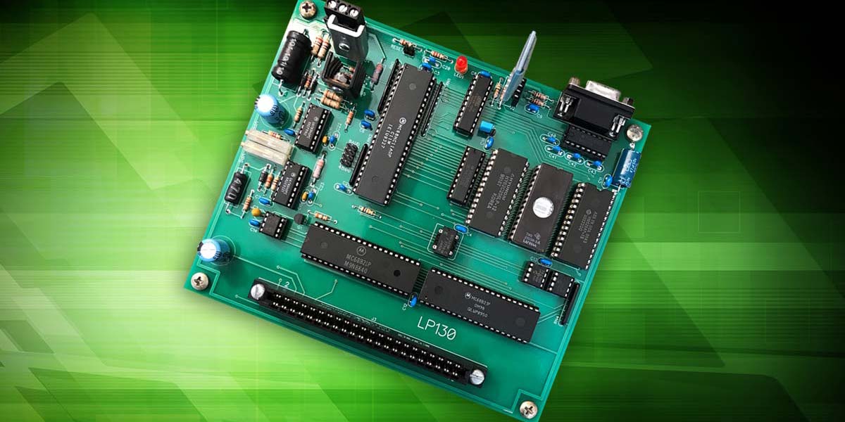
The LP130 is a highly flexible system (Figure 8).
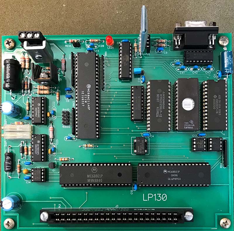
FIGURE 8. Finished LP130 circuit board.
It provides the circuitry needed to program programmable chips and firmware tools to assist writing device drivers. While I do all my programming in assembly language, you could use any language compiler compatible with the 68HC11 to write device drivers.
As an example of its flexibility, I created a plugin module and wrote the driver to test RAM and logic chips. NV
Parts List
| Qty |
Reference |
Part |
| Semiconductors |
| 2 |
D1, D2 |
1N5819, 40V Schottky Diode |
| 1 |
D3 |
1N5818, 30V Schottky Diode |
| 1 |
Q1 |
2N2907A, TO-92, PNP |
| 1 |
Q2 |
2N3906, TO-92, PNP |
| 1 |
Q3 |
2N3904, TO-92, NPN |
| 2 |
Q4, Q5 |
TIP30, TO-220, PNP |
| 1 |
U1 |
MC68HC11A0P, Microcomputer |
| 1 |
U2 |
74HCT573, Octal Transparent Latch |
| 1 |
U3 |
62256, 32K x 8 CMOS RAM |
| 1 |
U4 |
27128, 16K x 8 EPROM |
| 1 |
U5 |
6264, 8K x 8 CMOS RAM |
| 1 |
U6 |
ATF16V8, Address Decoder |
| 2 |
U7, U8 |
68B21, Peripheral Interface Adapter |
| 2 |
U10, U11 |
23LC1024, 128K x 8 SPI Serial RAM |
| 1 |
U12 |
MCP4802, Dual 8-bit SPI Serial DAC |
| 2 |
U13, U14 |
78S40, Universal Switching Regulator |
| 1 |
U40 |
MAX232, RS-232 Interface |
| 1 |
Y1 |
.3728 MHz Oscillator |
| Capacitors |
| 1 |
C1 |
47 µFd, 35V, Axial |
| 1 |
C2 |
4.7 µFd, 35V, Radial, 0.1”, Tantalum |
| 13 |
C3-C14, U9 |
0.1 µFd, 35V, Radial, 0.1” |
| 1 |
C15 |
560 pFd, 35V, NPO, Radial, 0.1” |
| 1 |
C16 |
680 pFd, 35V, NPO, Radial, 0.1” |
| 1 |
C18, C19 |
100 µFd, 50V Radial Electrolytic |
| 8 |
C20-C43 |
1 µFd, 35V Radial, 0.2” |
| Resistors (0.25W, 5% unless noted otherwise) |
| 2 |
R1, R2 |
220 ohm (red-red-brown-gold) |
| 1 |
R3 |
390 ohm (orange-white-brown-gold) |
| 2 |
R4, R5 |
820 ohm (gray-red-brown-gold) |
| 1 |
R6 |
2.2K (red-red-red-gold) |
| 1 |
R7, R8 |
270 ohm, 0.5W (red-violet-brown-gold) |
| 2 |
R9, R19 |
1K, 3/4”, 15+ turn Trimmer |
| 3 |
R10, R17, R20 |
1K (brown-black-red-gold) |
| 2 |
R11, R18 |
0.33 ohm, 0.5W (orange-orange-silver-gold) |
| 2 |
R12, R23 |
3.3K (orange-orange-red-gold) |
| 2 |
R13, R15 |
180, 0.5W (brown-gray-brown-gold) |
| 1 |
R14 |
27K (red-violet-orange-gold) |
| 1 |
R16 |
4.7K (yellow-violet-red-gold) |
| 1 |
R21 |
2.7K (red-violet-red-gold) |
| 1 |
R22 |
3.0K (orange-black-red-gold) |
| 1 |
R24 |
10K (brown-black-orange-gold) |
| 2 |
R40, R41 |
1.1K (brown-brown-red-gold) |
| 2 |
RN1, RN2 |
10K, SIP-10, Pin 1 Common |
| 2 |
RN3, RN4 |
10K, SIP-8, Pin 1 Common |
| Sockets |
| 2 |
U1 |
DIP-24, 600 mil |
| 2 |
U2, U6 |
DIP-20, 300 mil |
| 3 |
U3, U5 |
DIP-28, 300 or 600 mil |
| 1 |
U4 |
DIP-28, 600 mil |
| 2 |
U7, U8 |
DIP-40, 600 mil |
| 3 |
U10, U11, U12 |
DIP-8, 300 mil |
| 3 |
U13, U14, U40 |
DIP-16, 300 mil |
| 1 |
Y1 |
DIP-8 Oscillator |
| Miscellaneous |
| 1 |
J1 |
3 x 0.2” (5.08 mm) Terminal Strip |
| 1 |
J2 |
4-pin Female Header for HC-06 |
| 1 |
J3 |
22/44 Edge Connector, 0.156” Contact x 0.2” Row Spacing |
| 1 |
J40 |
DB-9S, Right Angle, PC Mount |
| 1 |
BAUD |
Double Row Jumper Header, 4 x 2 |
| 2 |
BT, RESET |
1 x 2 Male Headers |
| 1 |
L1 |
100 µH Coil |
| 1 |
L2 |
47 µH Coil |
| 1 |
LED1 |
T1.75 LED |
| 672 |
|
Shorting Jumpers |
Resources
The LP130 is available from Lucid Technologies at https://lucidtechnologies.info. Send questions or comments to [email protected].
Internet Resources
Freeware 68HC11 Cross-Assemblers
https://www.gnu.org/software/m68hc11
Object File Translator and Tools
https://lucidtechnologies.info/software.htm
Tera Term
https://en.wikipedia.org/wiki/Tera_Term
https://ttssh2.osdn.jp/index.html.en