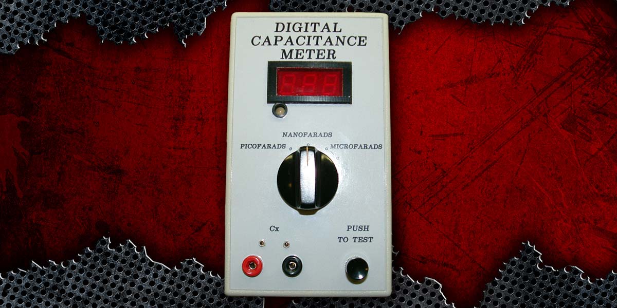
Over the years, I have amassed quite a selection of air variable capacitors and trimmers. Starting a project that used one of these devices used to feel like it required an Act of Congress to select the right one, since they were of unknown values. I finally decided it was time to add a capacitance meter to my test bench. However, I couldn’t justify the cost ($100+), so I decided to build my own.
Reviewing published designs of capacitance meters from the last 20+ years, I found that most had flaws that included poor linearity, poor accuracy, and volatile test leads (could blow out internal ICs if shorted together). Some of the designs were superb in resolution and low-end range, reaching well into the femtofarad region. However, their complexity did not justify their extreme accuracy, which was well beyond test-bench needs.
Requirements
At that point, I decided to design my own unit from scratch. My initial prerequisites would be:
- Minimal range switching for an adequate span of measurements
- No precision components required
- Minimal adjustments
- Decent accuracy and stability
- Battery operation
The completed unit fulfills these requirements. Its accuracy is as good as its resolution will allow and as good as the standard it is calibrated to. Overlap has been provided on all ranges except for the lowest one to help alleviate this problem. It has been my experience that once you get below 10 pF (the worst case resolution here), the physical circuit pretty much dictates the values needed. This is usually the case of adding “a little more or a little less” from the design-center values. Consider this: The average PN junction has a capacity of 5 pF and varies with the voltage across it, making it difficult to predict exactly how it will behave in the finished circuit. Circuit boards and layout can add another 1-5 pF between nodes, which are even more difficult to predict. It is for this reason I decided not to go beyond tenths of picofarads resolution.
The final design then spec’ed out as follows:
- Four ranges:
– 0-999 pF
– 0-99.9 nF
– 0-9.99 µF
– 0-999 µF
- Four calibration adjustments
- One “zero” adjustment
- No precision components used
- Nine-volt battery operation
- Well beyond 1% accuracy
Theory of Operation
Before I get into construction, I want to give a detailed theory of operation that will also be handy for troubleshooting, if necessary. The heart of this design is U1, an LM311 comparator. Normally the output of U1-p7 is high. When a capacitor is inserted in the Cx test jacks, it begins charging toward the p7 positive voltage through its range-timing resistor (R8, R9, R10). Cx is also connected to the negative input of U1 (p3). When this voltage rises above the reference voltage on p2 (the positive input), the comparator trips and U1-p7 goes low.
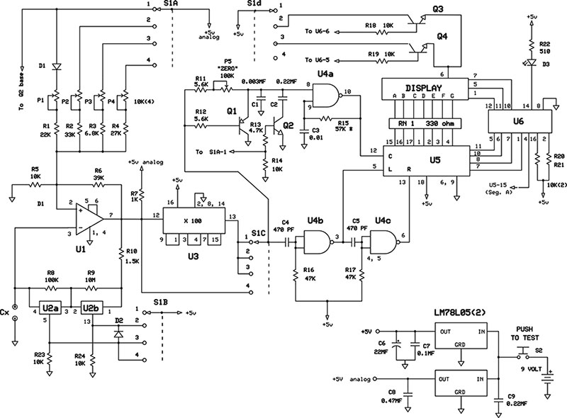
The schematic.
Now, Cx starts to discharge through the same timing resistance to this new low voltage. The positive input has also immediately dropped to a lower voltage at this time due to feedback resistor R6. U1-p2, the reference voltage, is now lower than Cx (U1-p3 negative input). Cx continues discharging until its voltage drops below the reference of U1-p2. At this point, the comparator trips, the output goes high, and the whole process starts all over again.
Resistors R5 and R6 provide a generous amount of hysterisis for fast switching, stability, and an adequate timing period. R1-R4, in conjunction with P1-P4, provide calibration for each range by setting the proper reference voltage at U1-p2. So basically what we have done is change a physical quantity (capacitance) to an electrical timing signal (period output at U1-p7).
All the component values mentioned so far were chosen to provide a 10.0 ms period at the output of U1-p7 for a full-scale reading on the three-digit display (999 > 000). This equates to 10 µs per count. For example, on the low range (0-999 pF), 1 pF = 1 µs and full scale equals 9.99 ms. This holds true for the first three ranges. Range four (0-999 mF) has a much longer period as will be explained shortly.
When I first constructed this unit, the timing resistors R8-R10 were connected directly to the switch S1B with two inch leads from the board, and I had all kinds of instability problems. This was caused by internal and external noise pickup on these leads. Surprisingly enough, these points were much more noise prone than the leads to Cx. For this reason, U2 (an analog switch) was added to provide switching right at the component location, which totally eliminated this problem. R23,24 ensure their control inputs remain at ground level when not activated. Diode D1 eliminates one switch pole by making S1A do double duty. This circuit is very accurate and linear throughout its range and has infinite resolution since it is basically an analog device.
However, there is a price to pay, and that is noise interference. Even a couple hundred microvolts of noise riding on the comparator inputs near the trip points can cause erratic readings on a digital display (wouldn’t be a problem with meter displays). But I have incorporated a couple of novel features downstream to almost totally eliminate erratic displays.
The first feature is U3 — a dual decade counter series wired up to give a divide-by-100 function. This, in effect, multiplies the period by 100 (remember that period is the reciprocal of frequency). This is beneficial in several respects. It greatly expands the gating period at its output, allowing not only the display’s latched count to hold longer, but also a slower more stable clock frequency (U4C). But above all, it provides 100-period averaging for U1’s output, and this greatly improves accuracy and stability in noisy environments.
So, up to this point we now have a period of 1.0 s at U3’s output for a full-scale output on the first three ranges. The output is a perfect square wave and the positive going portion will be used as the gate pulse for the clock. On range four (0-999 mF), this divider is bypassed as the time constant requirement for this range is so long that by proper design its gating pulse can go directly to S1C, which selects the proper gating pulse for the range used.
In all cases, we want a 500 ms positive pulse here representing full scale for any range. This gating pulse will drive two circuits from this point. One of these is the circuitry of Q1,Q2. This is a variable delay circuit for zeroing parasitic (stray) capacitance. The positive going edge of the gate pulse is integrated by the combination of R11, P5, C2 before driving the clock oscillator U4A. This delays the start of the clock oscillator which is the second novel feature, as mentioned previously. Instead of merely gating a free running clock oscillator for count pulses, the incoming gate actually starts and stops the oscillator.
When the incoming integrated pulse reaches sufficient amplitude, it instantly starts up the clock oscillator and runs it for that duration. We can get away with a slow rising logic pulse at this point due to the fact that these NAND gates have Schmidt triggers built into their inputs. Also, the clock oscillator can be a one-stage device for the same reason.
By gating the clock in this fashion we eliminate “clock walk through” and its annoying display jitter. “Clock walk through” occurs when the start of a gate can occur at any point in a free-running clock cycle, thereby producing a marching pattern through it. This alternatively affects the display’s LSB, causing the “±1 digit” commonly seen in counter specifications. By locking the two together, this is eliminated. U4A is a 2 kHz clock producing 1,000 count pulses in a 500 ms gate period, giving a display of 999 > 000, for a full-scale reading. The clock pulses from here are fed to U5-p12 clock input to operate this device.
Now, let’s back up for a moment to the Q1,Q2 delay circuit. This circuit operates only on range one (0-999 pF). We neither need it nor desire it on the other ranges. This is accomplished by turning on Q2 and enabling C2 to ground. Q2 is turned on when the range switch S1A is in the first range by applying +5 V into its base through R13 . Diode D1 isolates this circuit from its associated calibration circuit. C1 provides a small residual delay for the other ranges. Q1 is turned on when the gate pulse goes negative, thereby giving the gate sharp turnoff characteristics and clearing this circuit to ground, setting it up for the next incoming gate pulse. The time constant of R11, P5, C2 determines the level of integration here and hence the amount of delay. P5 now essentially becomes a zeroing control, blocking parasitic capacitance that would otherwise show up on the display. This control has a range of 0-50 pF for zeroing out both internal and external capacitance. This unit will have about 20 pF of internal parasitics to zero out, leaving about 30 more for external parasitics. If desired, P5 could be front-panel mounted, but you will need at least a 10 turn pot for this control.
Returning to the gate output at S1C, when this pulse goes low, U4A stops and the total count is registered in U5’s counter circuitry. The negative gate portion fed to U4B is highly differentiated by the time constant of C4, R16 producing a 20 µs positive pulse at its output. This pulse is fed to U5-p5 and latches its stored count into the display. At the same time, the negative-going edge of this pulse drives U4C through C5, R17 and its operation is identical to U4B. Again, there’s a 20 µs positive pulse, but delayed 20 µs from U4B’s. This pulse drives U5-p13 and resets the counter circuitry to zero, readying these stages for the next gated counting cycle.
U5 is a four-digit counter with multiplexed output drivers. The last digit (MSB) is not used as we only have a three-digit display. The common segment drivers are current limited through RN1, a 330 W DIP package. The common cathodes of the display are driven through U6, a high current, seven-pack inverter.
One annoying feature of the display I used is that the decimal points are also multiplexed. The only way to separate these is with the decoding circuitry of Q3, Q4. If you use a display where the decimal points are individually accessible, you can eliminate this nonsense and run them directly to S1D through suitable current limiting resistors (510 W).
I had neither the room nor the desire to add another chip for overflow circuitry. However, there were three idle inverters in U6 that weren’t earning their keep. I wired these up logically to look for a loss of segment “a” at the same time digit “A” was active. Half baked? Yeah, but it does work for the first overflow cycle and takes up almost no additional board real estate. This will at least confirm that when the display reads “000,” it’s either at full scale or there’s no capacitance at all!
You will also note that there are two +5 V supplies. One of these (+5 V analog) is reserved exclusively for the LM311 (U1), which needs very quiet supply lines to operate properly. Although I show one high-frequency bypass capacitor on the supply lines, in practice, I always use several — usually one for every three or four chips and also at the end of long (three inches or so) supply traces.
Construction
At this point, you should have a good understanding of the circuit and the confidence to build it, so now I will go into the construction details.
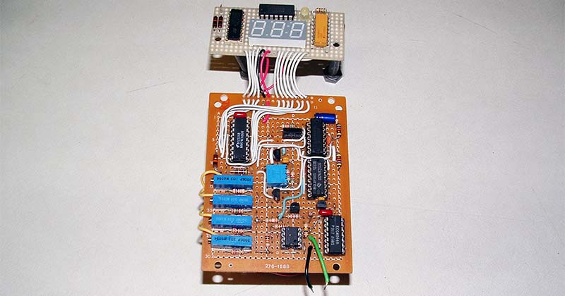
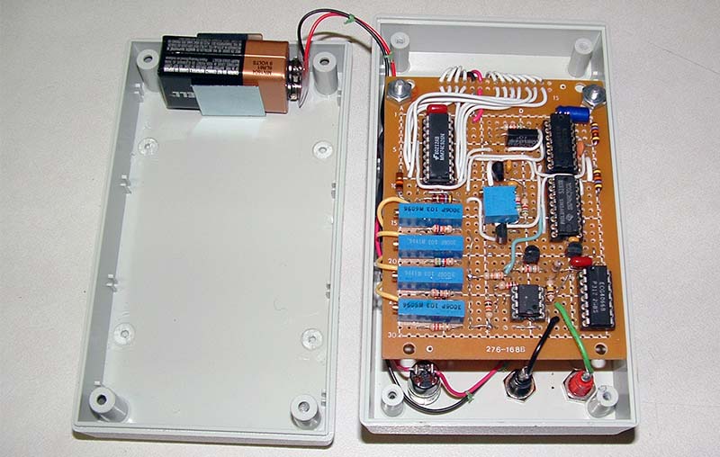
The circuitry was built on two boards. One was 1-1/4” x 3” perf board, hand-wired for the display, U6, RN1, Q3, and Q4. The other was the main board 2-3/4” x 3-7/8”. The display board gets folded back and mounted on the same threaded standoffs as the main board with proper spacers. I used a plastic housing that’s common to BUD and SERPAC.
Once the timing resistor switching (R8-R10) is done, using U2, there is no more critical wiring to do. Just keep U1’s inputs (p2, p3) short and in the clear as much as possible.
The 2 kHz clock oscillator (U4A) can be adjusted to the correct frequency with R15. This does not need to be exact: plus or minus 20 Hz is adequate. Use two resistors here. One will be as large as you can go without going over the target frequency, the other will be a small value to fine-tune it. I used a 51 kW in series with a 6.2 kW and came within 2 Hz of the 2 kHz target. All resistors are 5% carbon film. R9 (10 MW) should be a 1% metal film, not for accuracy, but for its stability. Carbon resistors with this high a value can have wild and unpredictable temperature coefficients. I used a 5% carbon film in this unit but will replace it the next time I have an order going out. These may be hard to find, but Newark Electronics has them.
The circuit boards.
Assembled and open.
Once the unit is completed, calibration is achieved by adjusting P1-P4 and P5. The nice feature about these calibration controls is that they compensate for all circuit component tolerances from their design centers including clock frequency error. Start by making a rough adjustment on the high end of each range. Then drop back to range one (0-999 pF) and adjust P5 (zero) to just eliminate any parasitic display to “000.” Now readjust P1 to whatever standard you are using. Then adjust ranges two through four to a standard on their high end.
You should now see “000” on all ranges with no capacitance in Cx. If ranges two through four show any parasitic reading, C1 will have to be tweaked somewhere between 2,000-5,000 pF. When making these tests, use the small test receptacles (A-29071-ND that are wired in parallel with Cx’s pin jacks) if possible. These will accept lead diameters of 0.20-.40 inches, which will accommodate 90% of tested capacitors. When necessary, use short leads out of the pin jacks and subtract any residual readings that these add (2-10 pF) before connecting the test capacitor.
For calibration, use the best standards you can scrounge up that are near the high end of each range. I am fortunate enough to own a 1% capacitor decade substitution box, but you can purchase 1% capacitors that will calibrate the two most critical ranges (one and two). These are 1,000 pF and 100 nF.
Calibrate, Test, Use
As opportunity presents, you can recalibrate with better standards on ranges three and four. This unit’s accuracy is only limited by the accuracy of the standards you calibrate it with. In my case, that was 1%, which is quite adequate for test bench use.
Although the display is quite stable, there will be instances where the Cx value is so close to the next whole digit (i.e., 99%), that it can cause LSB flicker. If that happens, simply move your free hand near the capacitor in Cx (2-3 inches) while reading the display. That will add that last fraction of a picofarad and stabilize the LSB to the next whole digit that it is already so close to.
The average current draw on this unit is about 35 mA, which is a pretty hefty load for a nine-volt battery. I ran accelerated life tests, assuming 1,000 tests per year at five seconds per test, and it appears the battery would last almost as long as its shelf life. For the front panel, I tried something new. I drew this up from one of my schematic CAD programs, along with text. I then printed this out on glossy photo paper and pasted it to the case with spray adhesive. Looks nice, but I don’t know how durable it will be. Time will tell, I guess. I built this unit for less than $30 and am very satisfied with it. The first tests I performed were to quantify and label all those air variable capacitors and trimmers. It was a breeze and a joy. NV
PARTS LIST
| RESISTORS |
VALUE |
|
|
| R1 |
22K |
|
|
| R2 |
33K |
|
|
| R3 |
6.8K |
|
|
| R4 |
27K |
|
|
| R5, 14, 18, 19, 20, 21, 23, 24 |
10K |
|
|
| R6 |
39K |
|
|
| R7 |
1K |
|
|
| R8 |
100K |
|
|
| R9 |
10M |
|
|
| R10 |
1.5K |
|
|
| R11, R12 |
5.6K |
|
|
| R13 |
4.7K |
|
|
| R15 |
57K* |
|
|
| R16, R17 |
47K |
|
|
| R22 |
510 |
|
|
| RN1 |
330 x 7 |
|
|
| HARDWARE |
|
|
|
| S1 |
Six pole-four pos |
|
|
| S2 |
P.B. NO |
|
|
| Pin Jacks |
|
|
|
| Miniature test jacks |
|
|
|
| CAPACITORS |
|
|
|
| C1 |
0.003 µF |
|
|
| C2, C9 |
0.22 µF |
|
|
| C3 |
0.01 µF |
|
|
| C4, C5 |
470 pF |
|
|
| C6 |
22 µF |
|
|
| C7 |
0.1 µF |
|
|
| C8 |
0.47 µF |
|
|
| POTENTIOMETERS |
|
|
|
| P1-P4 |
10K/15T |
|
|
| P5 |
100K/15T |
|
|
| SEMICONDUCTORS |
|
|
|
| D1, D2 |
1N914 |
|
|
| D3 |
LED five milliamp |
|
|
| Q1 |
2N3906 |
|
|
| Q2-Q4 |
2N3904 |
|
|
| U1 |
LM311 |
|
|
| U2 |
CD4066 |
|
|
| U3 |
74HC390 |
|
|
| U4 |
74HC132 |
|
|
| U5 |
74C926 |
|
|
| U6 |
ULN2003 |
|
|
| Display |
Three-digit MX |
Digi-Key |
160-1545-5-ND |