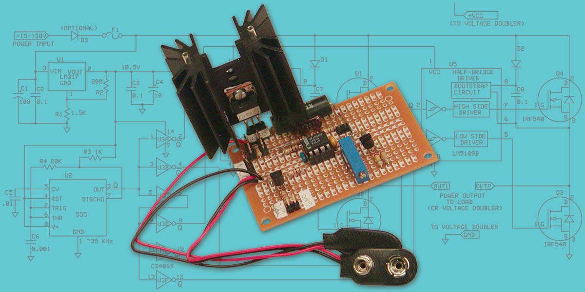
Part 2: Projects
Last time, we examined how to use power MOSFETs. This time, we'll build two projects. The first is a transformerless voltage doubler that takes a DC voltage from 12 to 30 volts and doubles it. Unlike most other voltage doubler circuits, this design can supply amps of current. It incorporates a high-efficiency, full-bridge design that has additional applications such as a motor driver, power inverter, or even a Class D power audio amplifier.
The second project uses a power MOSFET in a linear (rather than switching) application. A simple constant current power supply is presented. With proper heatsinking, it can supply up to 20 amps. Each project can be built at a basic parts cost of about $15.
The H-bridge
The voltage doubler is based on a standard H-bridge design, shown in Figure 1.
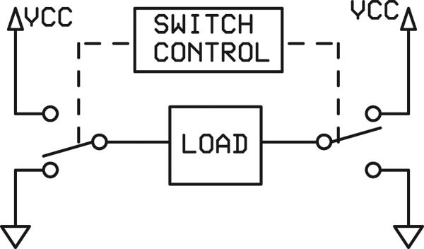
FIGURE 1. Conceptually, an H-bridge is just a double-pole, double-throw switch that reverses the polarity of the power to the load.
Basically, an H-bridge functions as a DPDT switch which reverses the polarity to a load. There are many applications for this circuit such as switching power supplies and motor control. Without getting into the details, switching at high speed gives good motor control and very efficient power supplies. The high frequency allows the use of smaller inductors and capacitors which can significantly reduce size, cost, and weight.
Our H-bridge is shown in Figure 2. It consists of several simple building blocks.
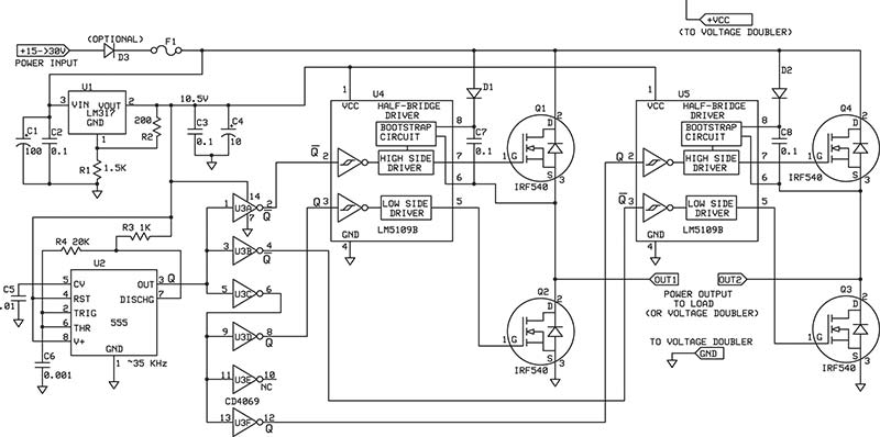
FIGURE 2. The basic H-bridge circuit. The power MOSFETS act as the DPDT switch. The control chips provide the proper gate voltages; the timer and inverter create the clock signals; and the voltage regulator sets a fixed voltage for the low voltage components.
The first is a regulated power supply (U1 and associated components). This is needed because other circuits may not be able to function over the full input range of the circuit. A three-terminal regulator is chosen to provide a stable 10.5 volts. Any voltage from 10 to 12 volts is fine for the low-power circuits. Generally, you want to keep it over eight volts for proper boot-strap operation (see Part 1). The other low voltage parts like to see something at 15 volts or less. A fixed 12 volt regulator (LM7812) can also be used here.
The second part is the master clock (U2 and associated parts) and is a simple 555 oscillator with a twist. As shown, it provides a very precise 50% duty cycle with a frequency of about 35 kHz. The twist is that the output pin is NOT used for the charging and discharging of the timing capacitor, as is the case for most other 50% duty cycle designs. This makes the circuit completely insensitive to output loading. Additionally, those other "50%" designs are more typically 45%-55%, or worse. Note that I verified proper operation with bipolar, CMOS, and low power 555 timer versions. A 50% duty cycle is not an absolute requirement for this design, but it distributes the power evenly through both halves of the bridge.
A DPDT switch makes and breaks contacts simultaneously (in theory). Since we are using N-channel parts for both the high side and low side, we will have to use a two phase clock. That is, both a "clock" signal and an "inverted clock" signal must be available. A CMOS 4069 inverter (U3) is used to invert the 555 signal. I chose to use separate inverters because they were available. You could run the Q signals directly from the 555 and the /Q inverted signals from a single inverter if desired.
As noted in Part 1, getting the power MOSFETs to switch quickly is not a trivial task. For that reason, I used special driver chips for this part of the circuit (U4 and U5). The LM5109 are inexpensive and easy to use. They provide a peak current of one amp to the gate of the MOSFET and typical switching times of 15 ns into 1,000 pF. They can support MOSFETs operating at up to 90 volts and can supply a bootstrap voltage of up to 108 volts. The Schmitt trigger inputs accept TTL and CMOS level signals.
Unfortunately, these drivers do not come in standard DIP packaging. I had to get SMT parts and fabricate an adapter as shown in Photo 1.
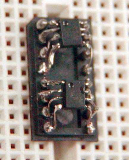
PHOTO 1. I made a DIP adapter for the surface mount drivers from a "component carrier." The large solder blobs on the carrier pins act as a heatsink when soldering to the driver chip. Once one pin is soldered, the rest go fairly easily.
It requires a steady hand with the soldering iron but is not too difficult. The trick is to put the component carrier in a protoboard (as shown) to support it and act as a heatsink for the pins. Put a blob of solder on a carrier pin and use #30 solid wire. Solder the carrier first because it acts as a heatsink. If you solder a wire to the SMT driver pin first, it may become unsoldered when you solder the wire to the carrier pin. Be careful with the heat because the carrier is made of thermoplastic and melts.
Last part of the circuit is the power MOSFETs themselves. I chose IRF540 devices. They cost about $0.75 each, operate up to 100 volts, and can handle 28 amps continuously with an on resistance of 0.77 ohms. In theory, this design can handle 2,500 watts of power. We won't be anywhere near that value.
The input voltage is limited to 30 volts because the voltage regulator that supplies power to the timer and other circuits is only rated at 35 volts. If you use a separate low-voltage power supply, the input can be theoretically increased to 90 volts where the driver chips fail. More realistically, the maximum safe input to the H-bridge is about 75 volts as shown.
The maximum continuous DC current — derated for heating — is about 14 amps for the MOSFETs. Since each MOSFET is on only 50% of the time and the switching speed is high, a full 28 amps through the bridge is a reasonable figure. Note that each MOSFET will have to dissipate 50 to 60 watts in this scenario, so good heatsinking will be a requirement.
Output Circuits and Variations
We will be using a simple capacitor voltage doubler, shown in Figure 3.
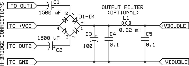
FIGURE 3. The voltage doubler circuit connects to the basic H-bridge (Figure 2) at four points. The output is close to a DC signal but switching glitches will be present. The optional filter (L2 and C3-C5) reduces the noise to about 200 mV.
It connects directly to the output of Figure 2. (In addition to the H-bridge outputs, connections to H-bridge power and ground are required.) Note that the doubled output voltage is theoretically a perfect DC signal right out of the bridge rectifier. In practice, switching glitches are present and can usually be removed with a simple filter as shown. The capacitor ratings in this voltage doubling circuit are critical. The use of improper capacitors can cause them to explode. (See the sidebar on Switching Capacitors for details.) Because of this failure possibility, it is strongly recommended that the project be housed in a sturdy box. Since the box only has input and output jacks, there seems little reason to show it.
If you want to do something other than voltage doubling, you can use Figure 4's circuit.
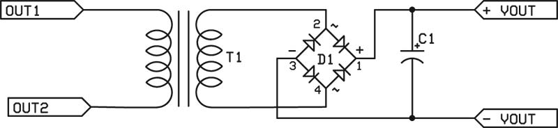
FIGURE 4. You can use a transformer to generate almost any voltage you want. The square wave input will require considerable output filtering, depending on the application. The transformer type and switching speed also have significant effects.
It's more conventional and easier to understand. Just remember that the switching frequency is 32 kHz, so ordinary 60 Hz transformers are marginal performers. (Of course, you can always change the circuit's frequency.) A toroidal transformer is usually incorporated here. Generally, they provide better efficiency and high frequency performance. I tried an ordinary 60 Hz power transformer and got reasonable results (considering the input was a square wave). Obviously, be sure your transformer is rated properly for current and voltage. Output filtering is required and is dependent on the frequency, transformer, and load.
A motor can be directly connected to the H-bridge. For optimal performance, you will want to be able to independently control the legs of the bridge. This cannot be done with a fixed oscillator. Instead, the Q and /Q signals should be adjustable. By changing the phase and pulse width, the motor's direction and speed can be controlled with precision. As noted above, if you want to use this H-bridge as a motor controller you should pay close attention to possible voltage and current spikes.
You can always use the H-bridge as an audio amplifier by attaching a loudspeaker to the output. This would be a "Class D" design where pulses are applied to the speaker. Again, the pulses would have to be precisely controlled, typically by a microcontroller. The high frequency pulses have to be filtered out to provide a low distortion audio signal. For good audio, the switching frequency should probably be increased to about 100 kHz. A Class D amplifier using this H-bridge has the potential of providing kilowatts of audio power (see the sidebar on Bridge Power).
Lastly, the circuit shown here operates at a nominal 35 kHz. By changing the timing capacitor in the 555 circuit, other frequencies can be obtained. There is a trade-off, however. The higher the frequency, the greater the switching losses. The capacitors and inductors (if used) can be smaller, though, which saves money and space. Additionally, the higher the operating frequency, the greater the likelihood of EMI (Electro-Magnetic Interference). Clearly, when you are switching kilowatts of power, you have to be concerned with unintentional RF (Radio Frequency) emissions. The square waves — so essential for efficiency — contain loads of higher frequency harmonics.
The Voltage Doubler Details
The design concept was to provide a simple voltage doubler for basic DC power supplies. In particular, I had a 0-30 volt, three amp supply. There are occasions when I needed a higher output voltage. Making the H-bridge voltage doubler is simplicity itself. Just connect two capacitors and a bridge rectifier as shown in Figure 3. The output will be a pretty good DC signal as shown in Photo 2.
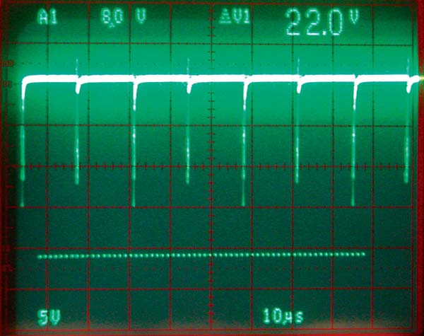
PHOTO 2. The output directly from the voltage doubler (without filtering) shows a DC signal with switching glitches. The simple filter shown in Figure 3 reduces these glitches to about 200 mV.
Only 165 nS switching glitches are present (photograph 3). These glitches can be reduced to about 200 mV with the optional output filter.
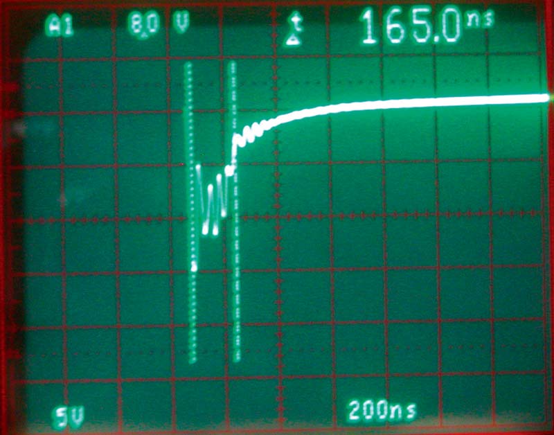
PHOTO 3. The switching glitch is about 165 ns. This can be reduced or eliminated with proper fine tuning of the switching signals.
Note that these glitches can be significantly reduced or even eliminated by fine-tuning the switch timing. Some driver chips allow this. Alternatively, you could use a microcontroller or dedicated digital hardware for better switching control.
Photo 2 shows that there are 22 volts out of the circuit with a 12 volt input. The circuit load was a 68 ohm resistor which pulled about 1/3 of an amp and dissipated over seven watts of heat. The MOSFETs weren't even warm. However, the bridge rectifier got quite hot because it was deliberately under-rated (will discuss shortly).
Photo 4 shows the breadboard of the voltage doubler. It's important to keep things as close together as practical.
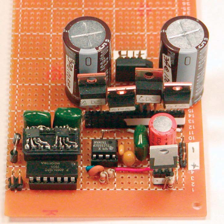
PHOTO 4. The breadboard of the voltage doubler (without filter). This is placed in a sturdy enclosure for safety (not shown, see text). Use short wires because the switching speeds are high.
Long leads with high frequencies can result in poor performance. Note that heatsinks for the MOSFETs are not needed for this typical operation of a few amps. I did not include the fuse because I will always be using it with a current-limited power supply. If you do not use such a supply, you should use a slow-blow fuse about 300% above the highest current output you expect. For example, if you power a device that draws one amp, use a three amp input fuse. This is because you will need more than twice the input current. The input diode (D3) is optional and is used to prevent damage if the input power is accidentally reversed. It will reduce the efficiency of the circuit. Make it about 10 times the expected output current with a PIV (Peak Inverse Voltage) of at least twice the maximum input voltage.
The major loss of power in the circuit is in the bridge rectifier. There is about 1.4 volts dropped across it. With an input voltage of 14 volts, at least 10% is lost here. With only one amp of current, it will have to dissipate 1.4 watts of power. For better heat control and efficiency, I recommend well oversized and separate diodes of 10-15 amps each with a heatsink (see Parts List). Using lower current diodes causes considerable heating which further increases the forward voltage drop. This causes even more heating and greater forward voltage drop, and so forth and so on. Losses can more than double if too small diodes are used. (Note that I only used a two amp bridge because I have a specific application that uses little power.)
Constant Current Supply
Power MOSFETs can be used in linear applications, as well. In such cases, they are typically treated as variable resistors which imply considerable heat losses. Proper heatsinking is necessary. Nevertheless, these devices allow you to control high power quite easily.
Figure 5 shows a simple constant current power supply. The theory of operation is very basic.
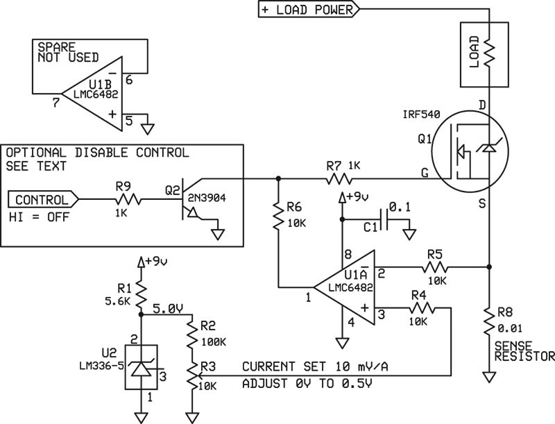
FIGURE 5. The analog constant current circuit is quite simple. A heatsink for the power MOSFET is required. For continuous use, R9 and Q2 can be omitted and R6 replaced with a wire.
A small voltage is developed across the 0.01 ohm sense resistor (R8) and is fed into the inverting input of the op-amp. This positive voltage is inverted by the op-amp, reducing the output voltage which reduces the voltage across the sense resistor via the MOSFET. This stabilizes the output voltage to the value found at the non-inverting input. Any change in current through the sense resistor causes a voltage change at the inverting input which is exactly offset by the negative feedback. The result is a constant current through the sense resistor and load.
Determining the reference voltage to be applied to the non-inverting input is just an application of Ohm's Law. If there is one amp of current flowing through the 0.01 ohm sense resistor, there will be 0.01 volts across it. So, the voltage-to-current ratio is 1:100 or 0.01 volts per amp.
The reference circuit is pretty straightforward. We want a stable and adjustable voltage from 0.0 volts to about 0.500 volts. I used an LM336-5 five volt reference because that is what I had on hand. Then, I reduced voltage with a resistor network and used a 10 turn trimmer for fine adjustment. Other methods of generating the reference voltage can be used, as well. (You can substitute an analog signal for the reference voltage and get a constant current power amplifier.)
There are a few considerations for this circuit. The first is that separate power supplies should be used for the load and circuit power. This is because it's very easy to cause significant power supply variations with 20 amps of current being drawn. If you choose to use a different op-amp, be sure it can operate with inputs very close to ground. The breadboard circuit is shown in Photo 5. The heatsink shown (a requirement) is rated at 13 watts.
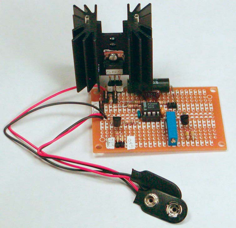
PHOTO 5.The breadboard of the constant current supply. Since the MOSFET is acting as a variable resistor, considerable heat is generated. A heatsink is required.
You may need a larger one for continuous use at 20 amps, depending on the load resistance. Remember that the MOSFET is acting like a resistor in this circuit. Depending on the load, its resistance can be relatively high or low and its power dissipation can be correspondingly high or low. Do the math to be sure. Note that at 20 amps, the five watt sense resistor (R8) dissipates four watts. If you plan on running this continuously at high current, you may want to increase R8 to seven or 10 watts.
Because of the very low sense resistance, ordinary circuit resistance can increase this significantly. (My circuit resistance was 30 milliohms.) The primary concern is that the voltage at the non-inverting input will be higher than expected (one amp per 13 mV rather than 10 mV). In most cases, this is not a problem for the proper operation of the circuit.
Since I didn't want to continuously run 20 amps while testing and for photography, I used a quick and dirty method of turning off the circuit. I simply used a transistor to pull the MOSFET gate to ground. This worked, but opened the feedback loop. As a result, when the transistor was turned off and normal linear operation was restored, there was considerable ringing as the loop re-stabilized. (If you don't want the disable control, you can eliminate R9 and Q2, and replace R6 with a wire.)
Photo 6 shows the circuit in operation. It is providing just about two volts into a 0.1 ohm load using a 14.4 volt portable tool battery. Thus, the current is about 20 amps. Not bad for a handful of components. In this 5% duty-cycle application, the heatsink was barely warm.
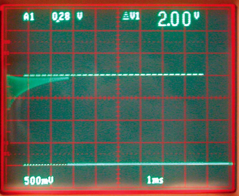
PHOTO 6. With a load of 0.1 ohms, this two volt signal means that 20 amps are flowing. The ringing is because the feedback loop was opened (see text).
Conclusion
Power MOSFETS can control a lot of power easily. An H-bridge voltage doubler circuit was seen to be suitable for this design, as well as other applications. An analog constant current project was able to easily provide 20 amps into a 0.1 ohm load. A nice feature of power MOSFETS is that if even higher currents are needed, they can be paralleled very easily. In short, power MOSFETs are an inexpensive and easy way of controlling significant power. NV
Switching Capacitor Ratings
It is extremely important to pay close attention to capacitor ratings in power switching circuits. These designs place a severe strain on the capacitor and it must be rated for this type of operation. Using the wrong type of capacitor can result in the capacitor exploding. Often, switching capacitors are chosen because of these other ratings rather than its capacitance. The two most important ratings to consider are: ESR and ripple current (typically at a switching frequency of 100 kHz). The ESR (Effective Series Resistance) says how much resistance the capacitor has. Ideally, a charge on one capacitor plate should freely interact with the other plate. But, capacitors 1 to 0.01 ohms. Everything else being equal, usually the larger the capacitor value is, the lower the ESR will be. So, if you are driving a heavy load (say a two ohm loudspeaker), a one ohm ESR will waste a lot of power and heat up the capacitor.
The second rating is the ripple current. This says how much RMS current can safely pass through the capacitor continuously. Again, typically, the larger the capacitor value, the higher current it can handle.
These capacitors usually fail because heat degrades the capacitor and increases the ESR. This causes a larger voltage drop across the capacitor and additional heating. Eventually, the capacitor gets too hot and bursts. This bursting can be mild or explosive. Most capacitors have relief points that reduce the chances of a violent explosion, but care should always be taken. Always house these types of circuits in a sturdy cabinet.
Bridge Power Ratings
In theory, a bridge circuit can provide up to four times more power to the load than a standard power control circuit. This seemingly impossible task is accomplished fairly directly and logically. However, it is a bit subtle. Suppose you have an ordinary audio amplifier running at eight volts and driving an eight ohm speaker. The voltage swing at the speaker will be a maximum of ±4 volts. Four volts into eight ohms is 0.5 amps. The peak output power is then two watts (Power = Current^2 x Resistance).
However, a bridge circuit changes the polarity to the load. This results in eight volts going in one direction and 8 volts going in the other direction for a ±8 volt swing. Doubling the voltage causes twice the current to flow, or one amp. Doubling the current results in four times as much power (P=I^2 x R). So, a bridge amplifier can provide up to four times as much power (eight watts) to the load as a non-bridge type.
The next question is why bridged power amplifiers are only rated at twice the non-bridged power, or less. This is because of the power handling of the amplifier rather than the theoretical power delivered to the load. If one amplifier can only dissipate enough heat to support X watts of power output, then two amplifiers can still only dissipate 2X watts, regardless of the voltage swing.
Constant Current Supply Parts List
| Resistors 1/4, 5% unless specified. |
| R1, R9 |
5.6K |
| R2 |
100K |
| R3 |
10K 10-turn trimmer |
| R4, R5, R6 |
10K |
| R7 |
1K |
| R8 |
0.01Ω 5W |
| Capacitors |
| C1 |
0.1 μF 25 volts |
| Semiconductors |
| Q1 |
IRF540 Power MOSFET |
| Q2 |
2N3940 NPN transistor |
| U1 |
LMC6482 Op-amp |
| Q2Q |
LM336-5 Five-volt reference |
| Misc: Heatsink for Q1 |
BASIC H-BRIDGE Parts LIST
| Resistors (1/4W, 5% unless specified) |
| R1 |
1.5K |
| R3 |
200 |
| R3 |
1K |
| R4 |
20K |
| Capacitors (25V unless specified) |
| C1 |
100 μF |
| C2, C3 |
0.1 μF |
| C4 |
10 μF |
| C5 |
0.01 μF |
| C6 |
0.001 μF |
| C7, C8 |
0.1 μF 150V |
| Semiconductors |
| D1, D2 |
1N4004 |
| D3 |
Optional, see text |
| Q1-Q4 |
IRF540 Power MOSFET |
| U1 |
LM317 adjustable voltage regulator |
| U2 |
555 timer |
| U3 |
CD4069 CMOS hex inverter |
| U4, U5 |
LM5109B half-bridge driver |
| Misc. |
| F1 |
Slow-blow fuse (see text) |
| Case |
Metal preferred for safety and EMI reduction (see text) |
| Additional parts for H-bridge Voltage Doubler (see text) |
| C1*, C2* |
1,500 μF 63 volt switching capacitor |
| D1-D4 |
15 amp rectifier (Jameco #879318) |
| C3 |
100 μF 150 volts (optional, see text) |
| C4, C5 |
0.1 μF 150 volts (optional, see text) |
| * Critical part, safety related, see text. |