Last time in this series, I described practical ways of using bipolar transistors in useful common-collector (voltage follower) circuit applications, including those of relay drivers, constant-current generators, linear amplifiers, and complementary emitter followers. This article moves on and shows various ways of using bipolar transistors in simple, but useful common-emitter and common-base configurations.
COMMON-EMITTER AMPLIFIER CIRCUITS
The common-emitter amplifier (also known as the common-earth or grounded-emitter circuit) has a medium value of input impedance and provides substantial voltage gain between input and output. The circuit’s input is applied to the transistor’s base, and the output is taken from its collector — the circuit’s basic operating principles were briefly described in the opening installment of this eight-part series. The common-emitter amplifier can be used in a wide variety of digital and analog voltage amplifier applications. This section of the Cookbook series starts off by looking at “digital” application circuits.
DIGITAL CIRCUITS
Figure 1 shows a simple npn common-emitter digital amplifier, inverter, or switch, in which the input signal is at either zero volts or a substantial positive value, and is applied to the transistor’s base via series resistor Rb, and the output signal is taken from the transistor’s collector. When the input is zero, the transistor is cut off and the output is at full positive supply rail value. When the input is high, the transistor is biased on and a collector current flows via RL, thus pulling the output low. If the input voltage is large enough, Q1 is driven fully on and the output drops to a “saturation” value of a few hundred mV. Thus, the output signal is an amplified and inverted version of the input signal.

FIGURE 1. Digital inverter/switch (npn)
In Figure 1, resistor Rb limits the input base-drive current to a safe value. The circuit’s input impedance is slightly greater than the Rb value, which also influences the rise and fall times of the output signal — the greater the Rb value, the worse these become. This snag can be overcome by shunting Rb with a “speed-up” capacitor (typically about 1n0), as shown dotted in the diagram. In practice, Rb should be as small as possible, consistent with safety and input-impedance requirements, and must not exceed RL x hfe.
Figure 2 shows a pnp version of the digital inverter/switch circuit. Q1 switches fully on, with its output a few hundred mV below the positive supply value, when the input is at zero volts, and turns off (with its output at zero volts) when the input rises to within less than 600mV of the positive supply rail value.
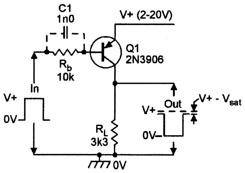
FIGURE 2. Digital inverter/switch (pnp)
The sensitivity of the Figure 1 and 2 circuits can be increased by replacing Q1 with a pair of Darlington- or Super-Alpha-connected transistors. Alternatively, a very-high-gain non-inverting digital amplifier/switch can be made by using a pair of transistors wired in either of the ways shown in Figures 3 or 4.
The Figure 3 circuit uses two npn transistors. When the input is at zero volts, Q1 is cut off, so Q2 is driven fully on via R2, and the output is low (saturated). When the input is “high,” Q1 is driven to saturation and pulls Q2 base to less than 600mV, so Q2 is cut off and the output is high (at V+).
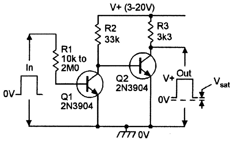
FIGURE 3. Very-high-gain non-inverting digital amplifier/switch using npn transistors
The Figure 4 circuit uses one npn and one pnp transistor. When the input is at zero volts, Q1 is cut off, so Q2 is also cut off (via R2-R3) and the output is at zero volts. When the input is “high,” Q1 is driven on and pulls Q2 into saturation via R3. Under this condition, the output takes up a value a few hundred mV below the positive supply rail value.
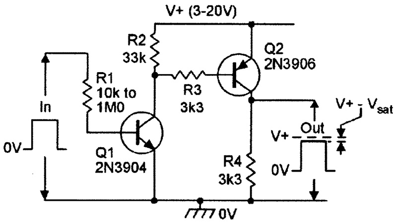
FIGURE 4. Alternative non-inverting digital amplifier/switch using an npn-pnp pair of transistors
Figure 5 shows (in basic form) how a complementary pair of the Figure 4 circuits can be used to make a DC-motor direction-control network, using a dual power supply. The circuit operates as follows.
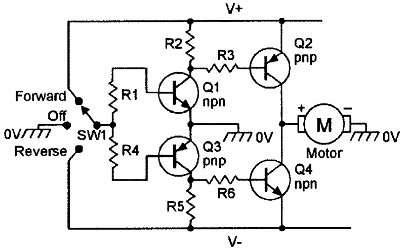
FIGURE 5. DC-motor direction-control circuit
When SW1 is set to “Forward,” Q1 is driven on via R1, and pulls Q2 on via R3, but Q3 and Q4 are cut off. The “live” side of the motor is thus connected (via Q2) to the positive supply rail under this condition, and the motor runs in the forward direction.
When SW1 is set to “Off,” all four transistors are cut off, and the motor is inoperative.
When SW1 is set to “Reverse,” Q3 is biased on via R4, and pulls Q4 on via R6, but Q1 and Q2 are cut off. The “live” side of the motor is thus connected (via Q4) to the negative supply rail under this condition, and the motor runs in the reverse direction.
RELAY DRIVERS
The basic digital circuits of Figures 1 through 4 can be used as efficient relay drivers if fitted with suitable diode protection networks. Figures 6 through 8 show examples of such circuits.
The Figure 6 circuit raises a relay’s current sensitivity by a factor of about 200 (= the current gain of transistor Q1), and greatly increases its voltage sensitivity. R1 gives base drive protection, and can be larger than 1k0, if desired. The relay is turned on by a positive input voltage.
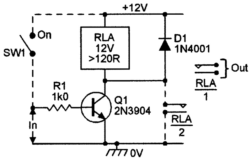
FIGURE 6. Simple relay-driving circuit
The current sensitivity of the relay can be raised by a factor of about 20,000 by replacing Q1 with a Darlington-connected pair of transistors. Figure 7 shows this technique used to make a circuit that can be activated by placing a resistance of less than 2M0 across a pair of stainless metal probes. Water, steam, and skin contacts have resistances below this value, so this simple little circuit can be used as a water, steam, or touch-activated relay switch.
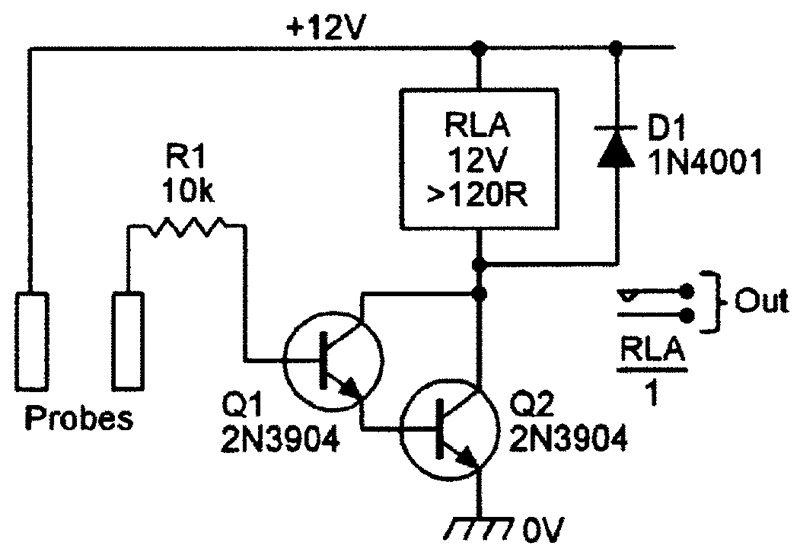
FIGURE 7. Touch, water, or steam-activated relay switch
Figure 8 shows another ultra-sensitive relay driver, based on the Figure 4 circuit, that needs an input of only 700mV at 40µA to activate the relay. R2 ensures that Q1 and Q2 turn completely off when the input terminals are open circuit.
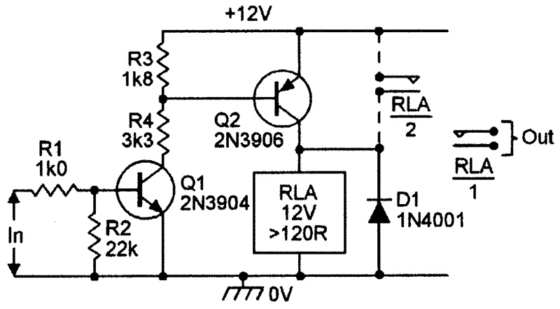
FIGURE 8. Ultra-sensitive relay driver (needs an input of 700mV at 40µA)
LINEAR BIASING CIRCUITS
A common-emitter circuit can be used as a linear AC amplifier by applying a DC bias current to its base so that its collector takes up a quiescent half-supply voltage value (to accommodate maximal undistorted output signal swings), and by then feeding the AC input signal to its base and taking the AC output from its collector (as shown in Figure 9).
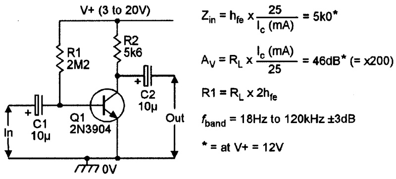
FIGURE 9. Simple npn common-emitter amplifier
The first step in designing a circuit of the basic Figure 9 type is to select the value of load resistor R2. The lower this is, the higher the amplifier’s upper cut-off frequency will be (due to the smaller shunting effects of stray capacitance on the effective impedance of the load), but the higher Q1’s quiescent operating current will be. In the diagram, R2 has a compromise value of 5k6, which gives an upper “3dB down” frequency of about 120kHz and a quiescent current consumption of 1mA from a 12V supply.
To bias the Figure 9 circuit’s output to half-supply volts, R1 needs a value of R2 x 2hfe, and (assuming a nominal hfe of 200) this works out at about 2M2 in the example shown. The formula for the circuit’s input impedance (looking into Q1 base) and voltage gain are both given in the diagram. In the example shown, the input impedance is roughly 5k0, and is shunted by R1 — the voltage gain works out at about x200, or 46dB.
The quiescent biasing point of the Figure 9 circuit depends on Q1’s hfe value. This weakness can be overcome by modifying the circuit as shown in Figure 10, where biasing resistor R1 is wired in a DC feedback mode between Q1’s collector and base, and has a value of R2 x hfe. The feedback action is such that any shift in the output level (due to variations in hfe, temperature, or component values) causes a counter-change in the base-current biasing level, thus tending to cancel the original shift.
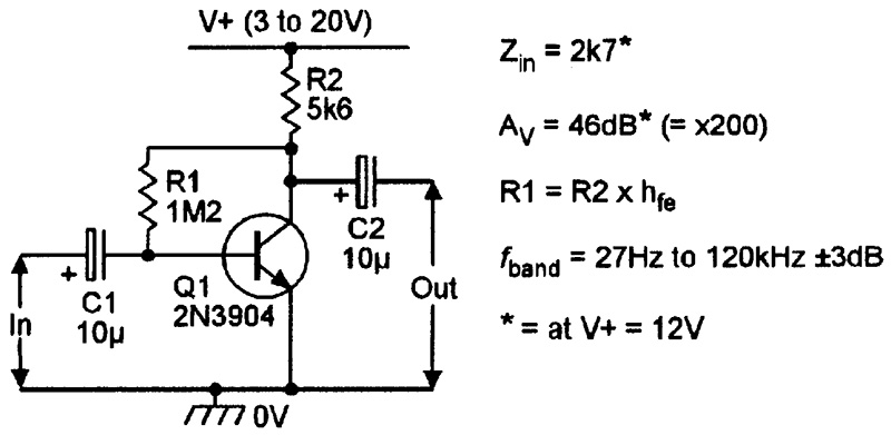
FIGURE 10. Common-emitter amplifier with feedback biasing
The Figure 10 circuit has the same values of bandwidth and voltage gain as the Figure 9 design, but has a lower total value of input impedance. This is because the AC feedback action reduces the apparent impedance of R1 (which shunts the 5k0 base impedance of Q1) by a factor of 200 (= AV), thus giving a total input impedance of 2k7. If desired, the shunting effects of the biasing network can be eliminated by using two feedback resistors and AC-decoupling them as shown in Figure 11.
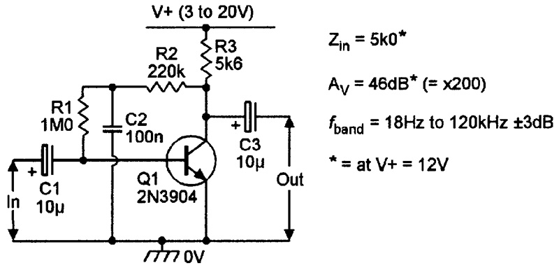
FIGURE 11. Amplifier with AC-decoupled feedback biasing
Finally, the ultimate in biasing stability is given by the “potential-divider biasing” circuit of Figure 12. Here, potential divider R1-R2 sets a quiescent voltage slightly greater than V+/3 on Q1 base, and voltage follower action causes 600mV less than this to appear on Q1 emitter. V+/3 is thus developed across 5k6 emitter resistor R3, and (since Q1’s emitter and collector currents are almost identical) a similar voltage is dropped across R4, which also has a value of 5k6, thus setting the collector at a quiescent value of 2V+/3. R3 is AC-decoupled via C2, and the circuit gives an AC voltage gain of 46dB.
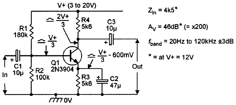
FIGURE 12. Amplifier with voltage-divider biasing
CIRCUIT VARIATIONS
Figures 13 to 16 show some useful common-emitter amplifier variations. Figure 13 shows the basic Figure 12 design modified to give an AC voltage gain of x10 — the gain actually equals the R4 collector load value divided by the effective “emitter” impedance value, which in this case (since R3 is decoupled by series-connected C2-R5) equals the value of the base-emitter junction impedance in series with the paralleled values of R3 and R5, and works out at roughly 560R, thus giving a voltage gain of x10. Alternative gain values can be obtained by altering the R5 value.
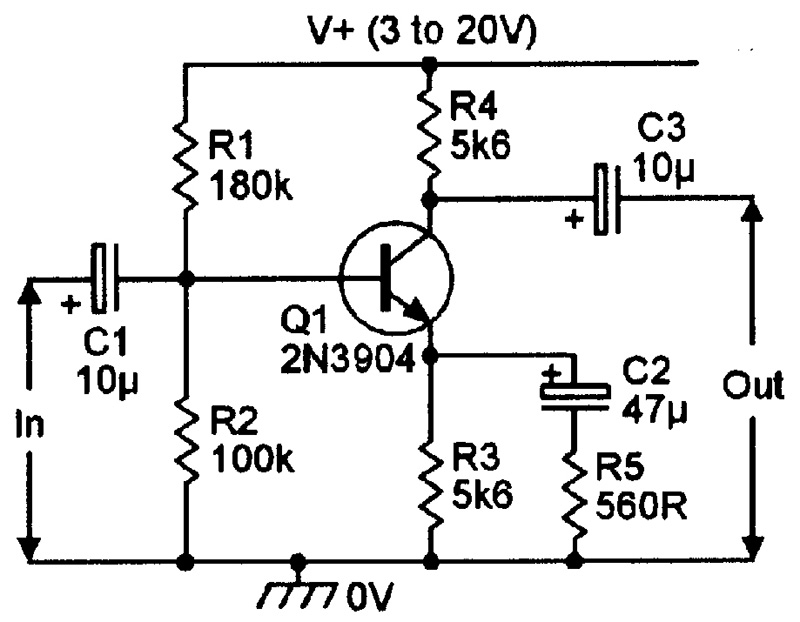
FIGURE 13. Fixed-gain (x10) common-emitter amplifier
Figure 14 shows a useful variation of the above design. In this case, R3 equals R4, and is not decoupled, so the circuit gives unity voltage gain. Note, however, that this circuit gives two unity-gain output signals, with the emitter output in phase with the input and the collector signal in anti-phase. This circuit thus acts as a unity-gain phase splitter.
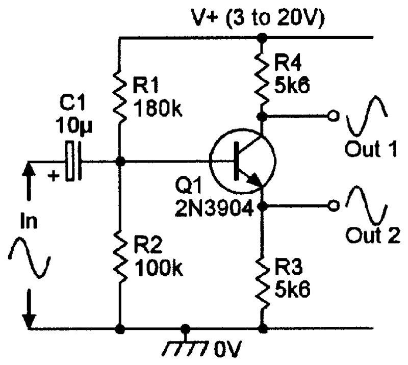
FIGURE 14. Unity-gain phase splitter
Figure 15 shows another way of varying circuit gain. This design gives high voltage gain between Q1 collector and base, but R2 gives AC feedback to the base, and R1 is wired in series between the input signal and Q1 base — the net effect is that the circuit’s voltage gain (between input and output) equals R2/R1, and works out at x10 in this particular case.
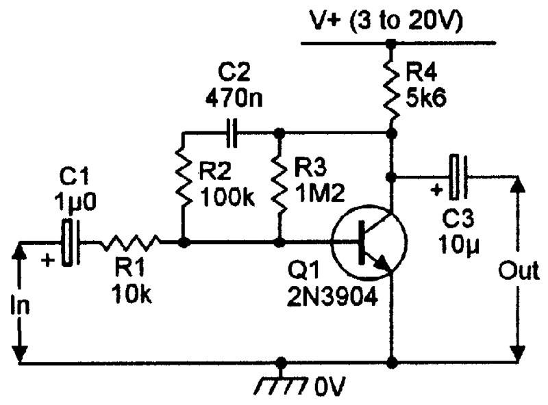
FIGURE 15. Alternative fixed-gain (x10) amplifier
Finally, Figure 16 shows how the Figure 10 design can be modified to give a wide-band performance by wiring DC-coupled emitter follower buffer Q2 between Q1 collector and the output terminal, to minimize the shunting effects of stray capacitance on R2, and thus extending the upper bandwidth to several hundred kHz.
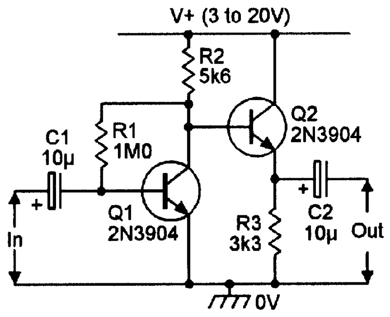
FIGURE 16. Wide-band amplifier
HIGH-GAIN CIRCUITS
A single-stage common-emitter amplifier circuit cannot give a voltage gain much greater that 46dB when using a resistive collector load — a multi-stage circuit must be used if higher gain is needed. Figures 17 to 19 show three useful high-gain, two-transistor voltage amplifier designs.
The Figure 17 circuit acts like a direct-coupled pair of common-emitter amplifiers, with Q1’s output feeding directly into Q2 base, and gives an overall voltage gain of 76dB (about x6150) and an upper -3dB frequency of 35kHz. Note that feedback biasing resistor R4 is fed from Q2’s AC-decoupled emitter (which “follows” the quiescent collector voltage of Q1), rather than directly from Q1 collector, and that the bias circuit is thus effectively AC-decoupled.
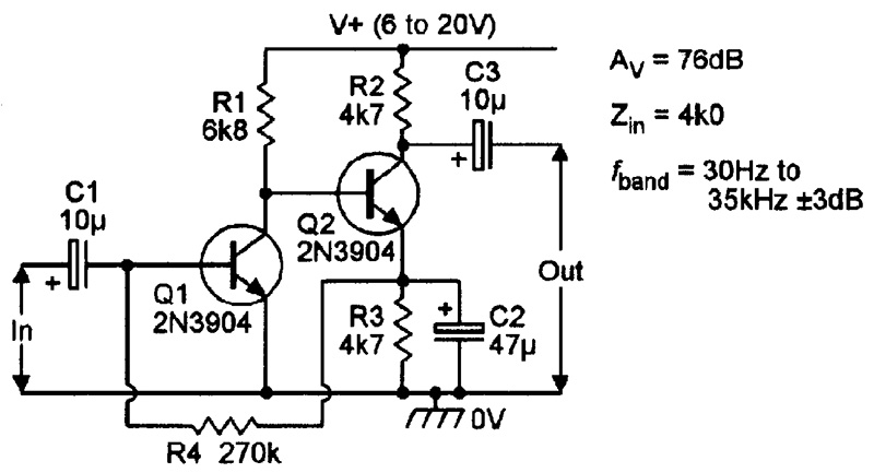
FIGURE 17. High-gain two-stage amplifier
Figure 18 shows an alternative version of the above design, using a pnp output stage — its performance is the same as that of Figure 17.
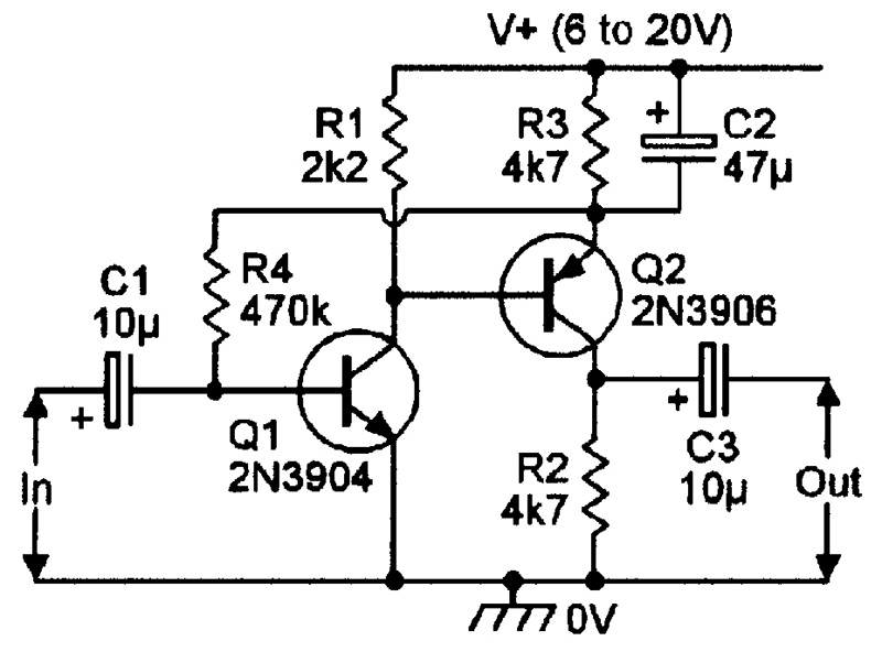
FIGURE 18. Alternative high-gain two-stage amplifier
The Figure 19 circuit gives a voltage gain of about 66dB. Q1 is a common-emitter amplifier with a split collector load (R2-R3), and Q2 is an emitter follower and feeds its AC output signal back to the R2-R3 junction via C3, thus “bootstrapping” the R3 value (as described in last month’s installment) so that it acts as a high AC impedance. Q1 thus gives a very high voltage gain. This circuit’s bandwidth extends up to about 32kHz, but its input impedance is only 330R.
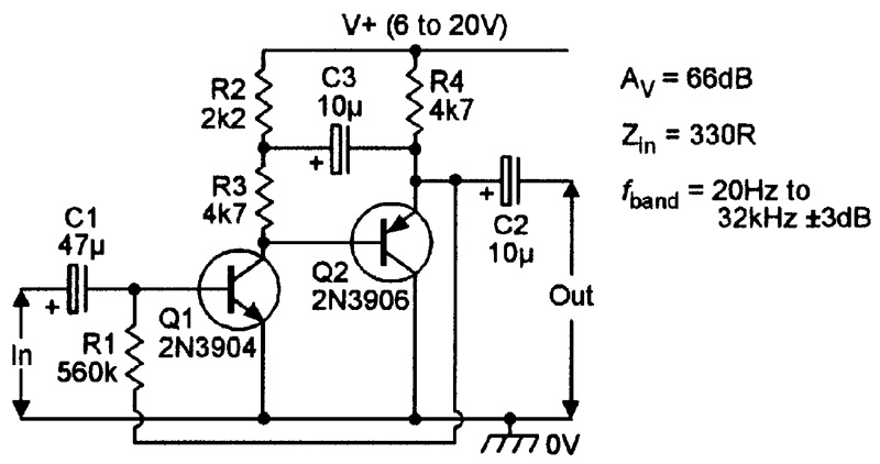
FIGURE 19. Bootstrapped high-gain amplifier
COMMON-BASE AMPLIFIER CIRCUITS
In a so-called “common-base” transistor amplifier, the input signal is applied to the transistor’s emitter, and the output is taken from the transistor’s collector. The common-base amplifier has a very low input impedance, gives near-unity current gain and a high voltage gain, and is used mainly in wide-band or high-frequency voltage amplifier applications. Figure 20 shows an example of a common-base amplifier that gives a good wide-band response.
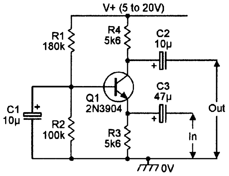
FIGURE 20. Common-base amplifier
The Figure 20 circuit is biased in the same way as Figure 12. Note, however, that the base is AC-decoupled via C1, and the input signal is applied to the emitter via C3. The circuit has a very low input impedance (equal to that of Q1’s forward-biased base-emitter junction), gives the same voltage gain as the common-emitter amplifier (about 46dB), gives zero phase shift between input and output, and has a -3dB bandwidth extending to a few MHz.
Figure 21 shows an excellent wideband amplifier — the “cascode” circuit — which gives the wide bandwidth benefit of the common-base amplifier, together with the medium input impedance of the common-emitter amplifier. This is achieved by wiring Q1 and Q2 in series, with Q1 connected in the common-base mode and Q2 in the common-emitter mode.
FIGURE 21. Wide-band cascode amplifier
The input signal is applied to the base of Q2, which uses Q1 emitter as its collector load and thus gives unity voltage gain and a very wide bandwidth, and Q1 gives a voltage gain of about 46dB. Thus, the complete circuit has an input impedance of about 1k8, a voltage gain of 46dB, and a -3dB bandwidth that extends to a few MHz.
Figure 22 shows a close relative of the common-base amplifier — the “long-tailed pair” phase splitter — which gives a pair of anti-phase outputs when driven from a single-ended input signal. Q1 and Q2 share a common emitter resistor (the “tail”), and the circuit bias point is set via RV1 so that the two transistors pass near-identical collector currents (giving zero difference between the two collector voltages) under quiescent conditions.
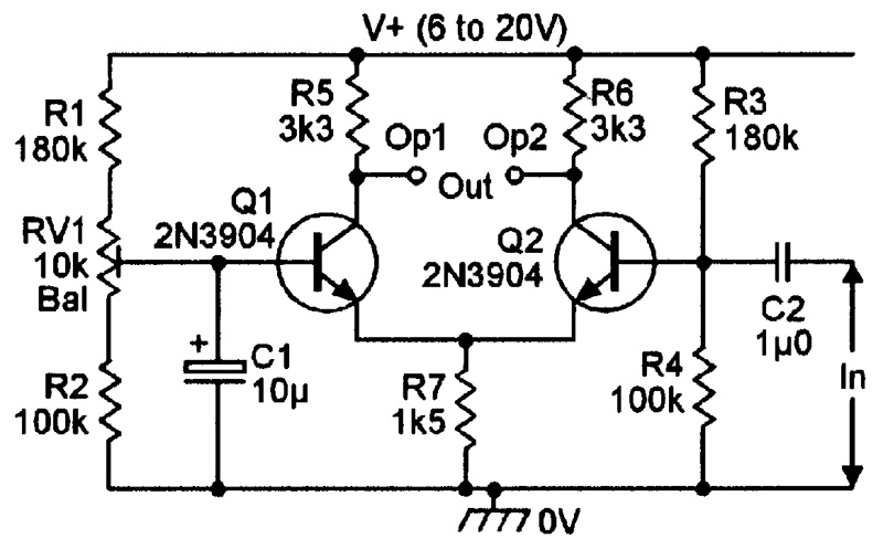
FIGURE 22. “Long-tailed pair” phase splitter
Q1 base is AC-grounded via C1, and AC-input signals are applied to Q2 base via C2. The circuit acts as follows.
Suppose that a sinewave input signal is fed to Q2 base. Q2 acts as an inverting common-emitter amplifier, and when the signal drives its base upward, its collector inevitably swings downward, and vice versa. Simultaneously, Q2’s emitter “follows” the input signal, and as its emitter voltage rises, it inevitably reduces the base-emitter bias of Q1, thus making Q1’s collector voltage rise, etc.
Q1 thus operates in the common-base mode and gives the same voltage gain as Q2, but gives a non-inverting amplifier action. This “phase-splitter” circuit thus generates a pair of balanced anti-phase output signals from a single-ended input.
Finally, Figure 23 shows how the above circuit can be made to act as a differential amplifier that gives a pair of anti-phase outputs that are proportional to the difference between the two input signals — if identical signals are applied to both inputs, the circuit will (ideally) give zero output.
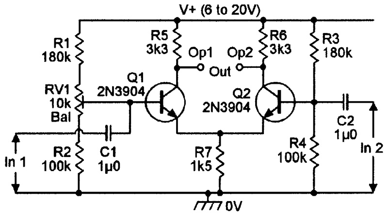
FIGURE 23. Simple differential amplifier or long-tailed pair
The second input signal is fed to Q1 base via C1, and the R7 “tail” provides the coupling between the two transistors. NV
