The two most widely used types of transistor waveform generator circuits are the oscillator types that produce sine waves and use transistors as linear amplifying elements, and the multivibrator types that generate square or rectangular waveforms and use transistors as digital switching elements.
This month’s installment describes practical ways of using bipolars in the linear mode to make simple, but useful sine wave and white-noise generator circuits. Next month’s edition of the series will deal with practical multivibrator types of bipolar waveform generator circuits.
OSCILLATOR BASICS
To generate reasonably pure sine waves, an oscillator has to satisfy two basic design requirements, as shown in Figure 1. First, the output of its amplifier (A1) must be fed back to its input via a frequency-selective network (A2) in such a way that the sum of the amplifier and feedback network phase shifts equals zero degrees (or 360°) at the desired oscillation frequency, i.e., so that x° + y° = 0° (or 360°). Thus, if the amplifier generates 180° of phase shift between input and output, an additional 180° of phase shift must be introduced by the frequency-selective network.
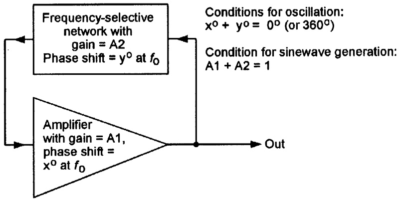
FIGURE 1. Essential circuit and conditions needed for sine wave generation.
The second requirement is that the amplifier’s gain must exactly counter the losses of the frequency-selective feedback network at the desired oscillation frequency, to give an overall system gain of unity, e.g., A1 x A2 = 1. If the gain is below unity, the circuit will not oscillate, and if greater than unity, it will be over-driven and will generate distorted waveforms. The frequency-selective feedback network usually consists of either a C-R or L-C or crystal filter; practical oscillator circuits that use C-R frequency-selective filters usually generate output frequencies below 500 kHz; ones that use L-C frequency-selective filters usually generate output frequencies above 500 kHz; ones that use crystal filters generate ultra-precise signal frequencies.
C-R OSCILLATORS
The simplest C-R sine wave oscillator is the phase-shift type, which usually takes the basic form as shown in Figure 2. Here, three identical C-R high-pass filters are cascaded to make a third-order filter that is inserted between the output and input of the inverting (180° phase shift) amplifier; the filter gives a total phase shift of 180° at a frequency, fo, of about 1/(14RC), so the complete circuit has a loop shift of 360° under this condition and oscillates at fo if the amplifier has enough gain (about x29) to compensate for the filter’s losses and, thus, give a mean loop gain fractionally greater than unity.
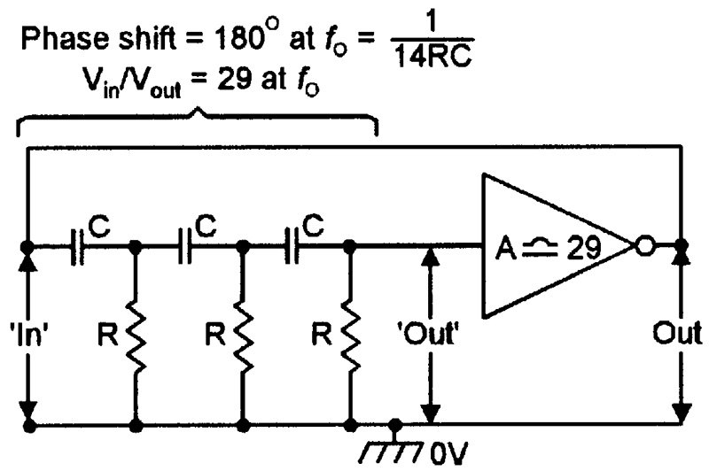
FIGURE 2. Third-order, high-pass filter used as the basis of a phase-shift oscillator.
Note in Figure 2 that each individual C-R high-pass filter stage tends to pass high-frequency signals, but rejects low-frequency ones. Its output is 3 dB down at a break frequency of 1/(2 RC), and falls at a 6 dB/octave rate as the frequency is decreased below this value. Thus, a basic 1 kHz filter gives 12 dB of rejection to a 250 Hz signal, and 20 dB to a 100 Hz one. The phase angle of the output signal leads that of the input and equals arctan 1/(2fCR), or +45° at fc. Each C-R stage is known as a first-order filter. If a number (n) of such filters are cascaded, the resulting circuit is known as an “nth-order” filter and has a slope, beyond fc of (n x 6 dB)/octave.
Figure 3 shows the circuit of a practical 800 Hz phase-shift oscillator that can operate from any DC supply in the 9V to 18V range. To initially set up the circuit, simply trim RV1 so that the circuit generates a reasonably pure sine wave output as seen on an oscilloscope — the signal’s output level is fully variable via RV2.
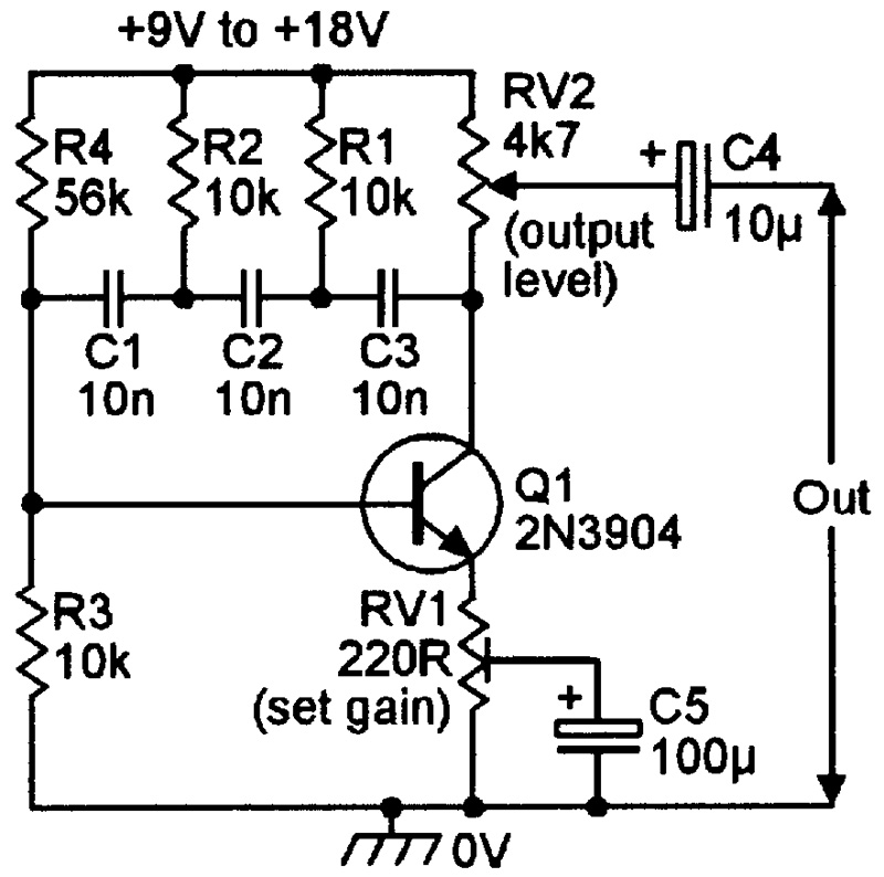
FIGURE 3. 800 Hz phase-shift oscillator.
Major disadvantages of simple phase-shift oscillators of the Figure 3 type are that they have fairly poor inherent gain stability, and that their operating frequency can not easily be made variable. A far more versatile C-R oscillator can be built using the Wien bridge network.
Figure 4 shows the basic elements of the Wien bridge oscillator. The Wien network consists of R1-C1 and R2-C2, which have their values balanced so that C1=C2=C, and R1=R2=R. This network’s phase shifts are negative at low frequencies, positive at high ones, and zero at a center frequency of 1/(6.28CR), at which the network has an attenuation factor of three. The network can thus be made to oscillate by connecting a non-inverting x3 high input impedance amplifier between its output and input terminals, as shown in the diagram.
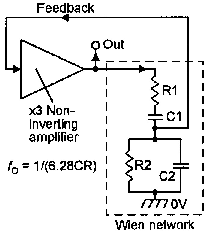
FIGURE 4. Basic Wien oscillator circuit.
Figure 5 shows a simple fixed-frequency Wien oscillator in which Q1 and Q2 are both wired as low-gain common-emitter amplifiers. Q2 gives a voltage gain slightly greater than unity and uses Wien network resistor R1 as its collector load and Q1 presents a high input impedance to the output of the Wien network and has its gain variable via RV1. The component values show that the circuit oscillates at about 1 kHz — in use, RV1 should be adjusted so that a slightly distorted sine wave output is generated.

FIGURE 5. Practical 1 kHz Wien oscillator.
Figure 6 shows an improved Wien oscillator design that consumes 1.8 mA from a 9V supply and has an output amplitude that is fully variable up to 6V peak-to-peak via RV2. Q1-Q2 are a direct-coupled complementary common-emitter pair, and give a very high input impedance to Q1 base, a low output impedance from Q2 collector, and non-inverted voltage gains of x5.5 DC and x1 to x5.5 AC (variable via RV1). The red LED generates a low-impedance 1.5V that is fed to Q1 base via R2 and therefore biases Q2’s output to a quiescent value of +5V. The R1-C1 and R2-C2 Wien network is connected between Q2’s output and Q1’s input, and in use RV1 is simply adjusted so that, when the circuit’s output is viewed on an oscilloscope, a stable and visually clean waveform is generated. Under this condition, the oscillation amplitude is limited at about 6V peak-to-peak by the onset of positive-peak clipping as the amplifier starts to run into saturation. If RV1 is carefully adjusted, this clipping can be reduced to an almost imperceptible level, enabling good-quality sine waves, with less than 0.5% THD, to be generated.
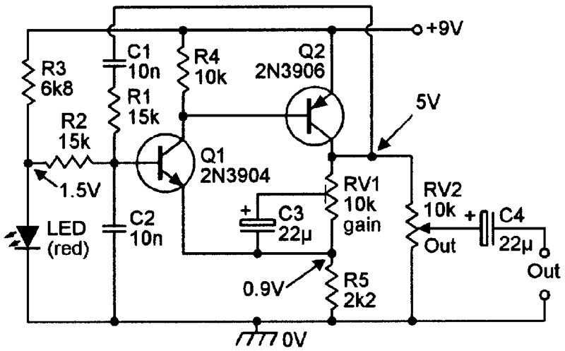
FIGURE 6. 1 kHz Wien bridge sine wave generator with variable-amplitude output.
The Figure 6 circuit can be modified to give limited-range variable-frequency operation by reducing the R1 and R2 values to 4.7K and wiring them in series with ganged 10K variable resistors. Note, however, that variable-frequency Wien oscillators are best built using op-amps or other linear ICs, in conjunction with automatic-gain-control feedback systems, using various standard circuits of this type that have been published in previous editions of this magazine.
L-C OSCILLATORS
C-R sine wave oscillators usually generate signals in the 5 Hz to 500 kHz range. L-C oscillators usually generate them in the 5 kHz to 500 MHz range, and consist of a frequency-selective L-C network that is connected into an amplifier’s feedback loop.
The simplest L-C transistor oscillator is the tuned collector feedback type shown in Figure 7. Q1 is wired as a common-emitter amplifier, with base bias provided via R1-R2 and with emitter resistor R3 AC-decoupled via C2. L1-C1 forms the tuned collector circuit, and collector-to-base feedback is provided via L2, which is inductively coupled to L1 and provides a transformer action. By selecting the phase of this feedback signal, the circuit can be made to give zero loop phase shift at the tuned frequency, so that it oscillates if the loop gain (determined by the turns ratio of T1) is greater than unity.
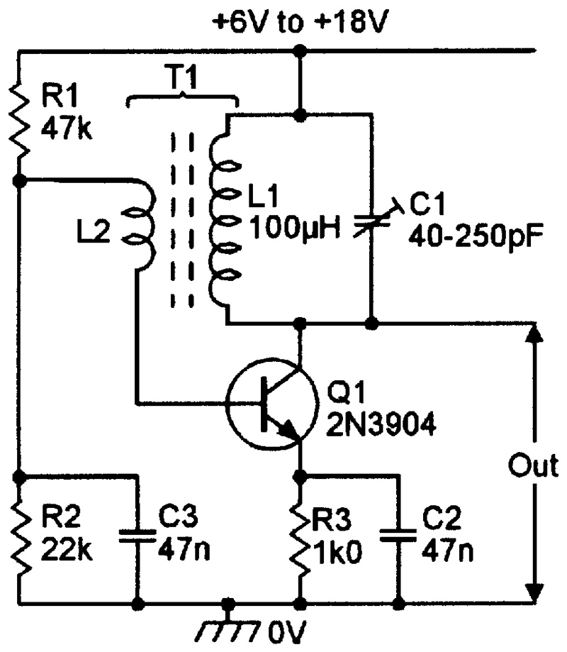
FIGURE 7. Tuned collector feedback oscillator.
A feature of any L-C tuned circuit is that the phase relationship between its energizing current and induced voltage varies from -90° to +90°, and is zero at a center frequency given by f = 1/(2 LC). Thus, the Figure 7 circuit gives zero overall phase shift, and oscillates at, this center frequency. With the component values shown, the frequency can be varied from 1 MHz to 2 MHz via C1. This basic circuit can be designed to operate at frequencies ranging from a few tens of Hz by using a laminated iron-cored transformer, up to tens or hundreds of MHz using RF techniques.
CIRCUIT VARIATIONS
Figure 8 shows a simple variation of the Figure 7 design — the Hartley oscillator. Its L1 collector load is tapped about 20% down from its top, and the positive supply rail is connected to this point; L1 thus gives an auto-transformer action, in which the signal voltage at the top of L1 is 180° out of phase with that at its low (Q1 collector) end. The signal from the top of the coil is fed to Q1’s base via C2, and the circuit thus oscillates at a frequency set by the L-C values.
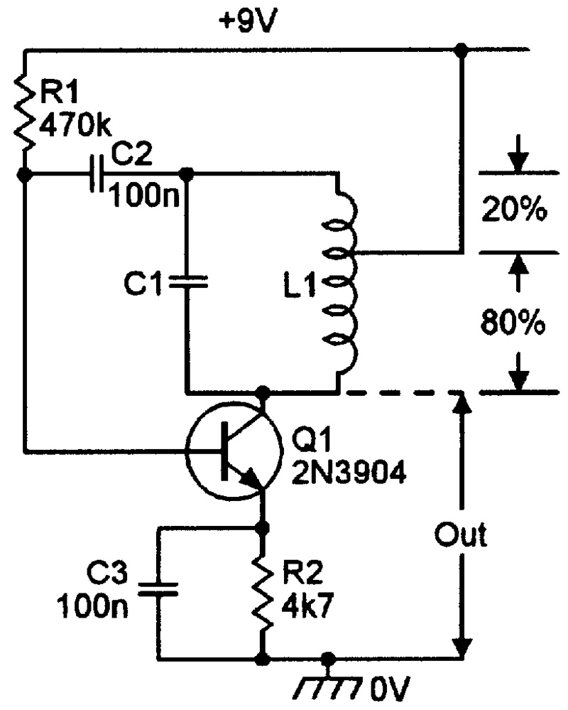
FIGURE 8. Basic Hartley oscillator.
Note from the above description that oscillator action depends on some kind of common signal tapping point being made into the tuned circuit, so that a phase-splitting autotransformer action is obtained. This tapping point does not have to be made into the actual tuning coil, but can be made into the tuning capacitor, as in the Colpitts oscillator circuit shown in Figure 9. With the component values shown, this particular circuit oscillates at about 37 kHz.
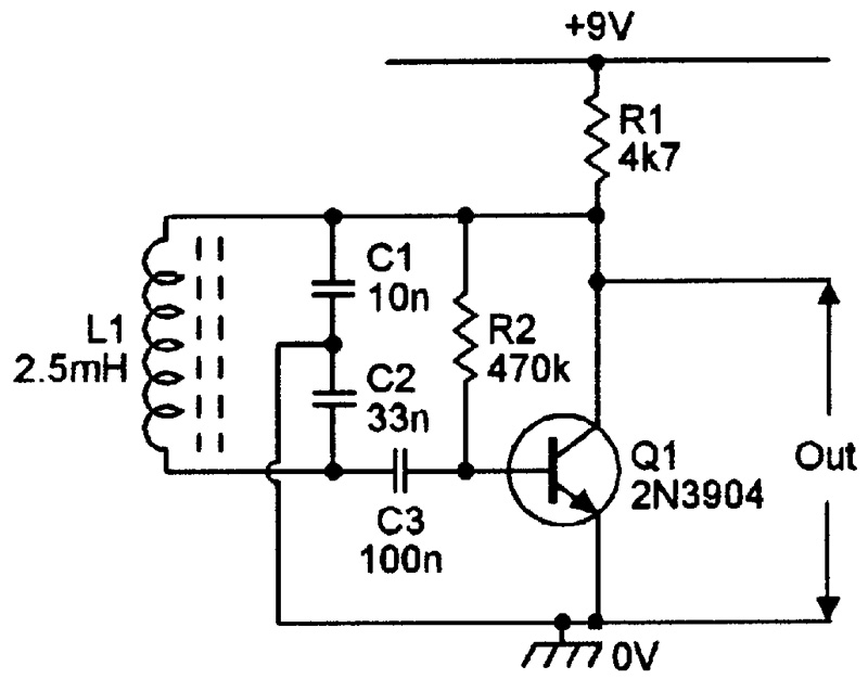
FIGURE 9. 37 kHz Colpitts oscillator.
A modification of the Colpitts design, known as the Clapp or Gouriet oscillator, is shown in Figure 10. C3 is wired in series with L1 and has a value that is small relative to C1 and C2. Consequently, the circuit’s resonant frequency is set mainly by L1 and C3, and is almost independent of variations in transistor capacitances, etc. The circuit thus gives excellent frequency stability. With the component values shown, it oscillates at about 80 kHz.
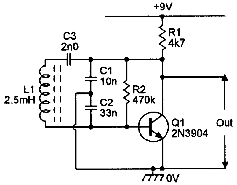
FIGURE 10. 80 kHz Gouriet or Clapp oscillator.
Figure 11 shows a Reinartz oscillator, in which the tuning coil has three inductively-coupled windings. Positive feedback is obtained by coupling the transistor’s collector and emitter signals via windings L1 and L2. Both of these inductors are coupled to L3, and the circuit oscillates at a frequency determined by L3-C1. The diagram shows typical coil-turns ratios for a circuit that oscillates at a few hundred kHz.
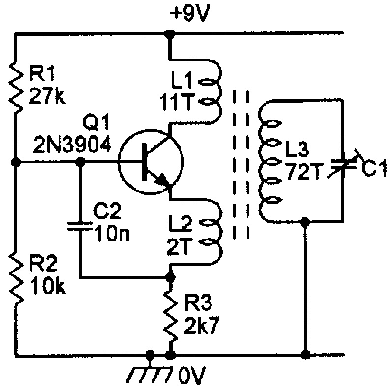
FIGURE 11. Basic Reinartz oscillator.
Finally, Figures 12 and 13 show emitter follower versions of Hartley and Colpitts oscillators. In these circuits, the transistors and L1-C1 tuned circuits each give zero phase shift at the oscillation frequency, and the tuned circuit gives the voltage gain necessary to ensure oscillation.
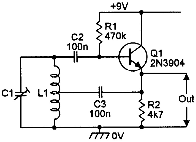
FIGURE 12. Emitter follower version of the Hartley oscillator.
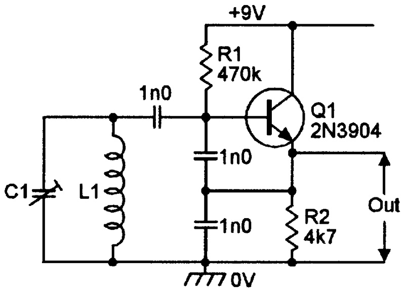
FIGURE 13. Emitter follower version of the Colpitts oscillator.
MODULATION
The L-C oscillator circuits of Figures 7 to 13 can easily be modified to give modulated (AM or FM) rather than continuous-wave (CW) outputs. Figure 14, for example, shows the Figure 7 circuit modified to act as a 456 kHz beat-frequency oscillator (BFO) with an amplitude-modulation (AM) facility. A standard 465 kHz transistor IF transformer (T1) is used as the L-C tuned circuit, and an external AF signal can be fed to Q1’s emitter via C2, thus effectively modulating Q1’s supply voltage and thereby amplitude-modulating the 465 kHz carrier signal. The circuit can be used to generate modulation depths up to about 40%. C1 presents a low impedance to the 465 kHz carrier but a high impedance to the AF modulation signal.
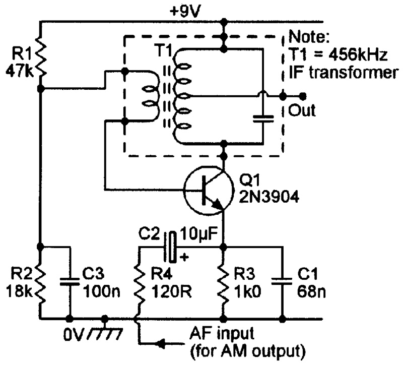
FIGURE 14. 465 kHz BFO with AM facility.
Figure 15 shows the above circuit modified to give a frequency-modulation (FM) facility, together with varactor tuning via RV1. 1N4001 silicon diode D1 is used as an inexpensive varactor diode which, when reverse biased (as an inherent part of its basic silicon diode action) inherently exhibits a capacitance (of a few tens of pF) that decreases with applied reverse voltage. D1 and blocking capacitor C2 are wired in series and effectively connected across the T1 tuned circuit (since the circuit’s supply rails are shorted together as far as AC signals are concerned).
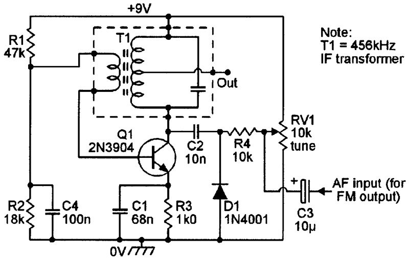
FIGURE 15. 465 kHz BFO with varactor tuning and FM facility.
Consequently, the oscillator’s center frequency can be varied by altering D1’s capacitance via RV1, and FM signals can be obtained by feeding an AF modulation signal to D1 via C3 and R4.
CRYSTAL OSCILLATORS
Crystal-controlled oscillators give excellent frequency accuracy and stability. Quartz crystals have typical Q values of about 100,000 and provide about 1,000 times greater stability than a conventional L-C tuned circuit. Their operating frequency (which may vary from a few kHz to 100 MHz) is determined by the mechanical dimensions of the crystal, which may be cut to give either series or parallel resonant operation. Series-mode devices show a low impedance at resonance — parallel-mode types show a high impedance at resonance.
Figure 16 shows a wide-range crystal oscillator designed for use with a parallel-mode crystal. This is actually a Pierce oscillator circuit, and can be used with virtually any good 100 kHz to 5 MHz parallel-mode crystal without need for circuit modification.
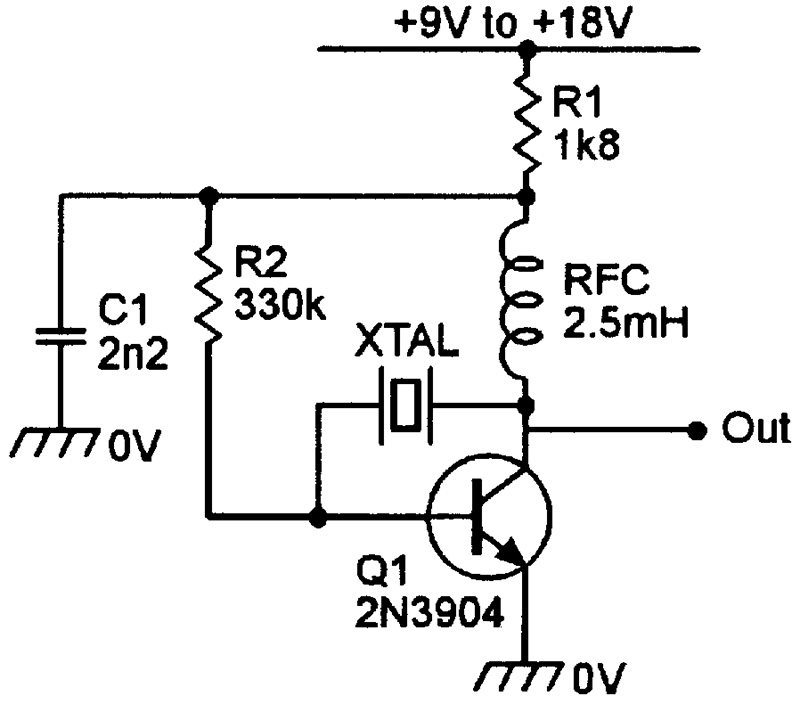
FIGURE 16. Wide-range Pierce oscillator uses parallel-mode crystal.
Alternatively, Figure 17 shows a 100 kHz Colpitts oscillator designed for use with a series-mode crystal. Note that the L1-C1-C2 tuned circuit is designed to resonate at the same frequency as the crystal, and that its component values must be changed if other crystal frequencies are used.
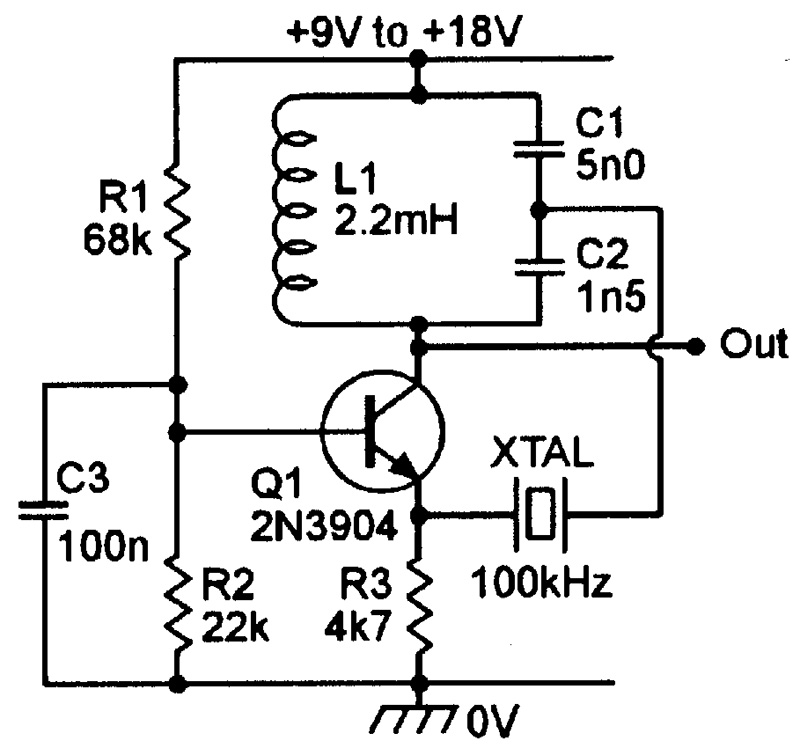
FIGURE 17. 100 kHz Colpitts oscillator uses series-mode crystal.
Finally, Figure 18 shows an exceptionally useful two-transistor oscillator that can be used with any 50 kHz to 10 MHz series-resonant crystal. Q1 is wired as a common-base amplifier and Q2 as an emitter follower, and the output signal (from Q2 emitter) is fed back to the input (Q1 emitter) via C2 and the series-resonant crystal. This excellent circuit will oscillate with any crystal that shows the slightest sign of life.
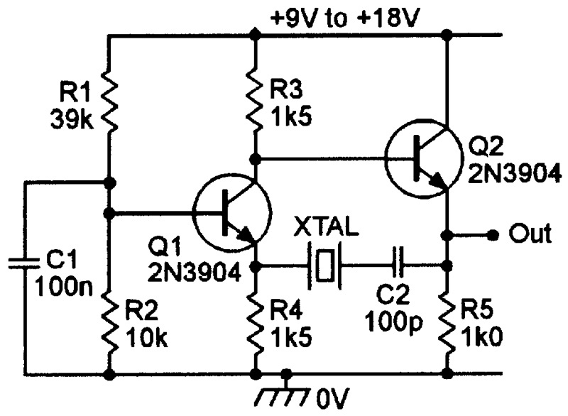
FIGURE 18. Wide-range (50 kHz-10 MHz) oscillator can be used with almost any series-mode crystal.
WHITE NOISE GENERATORS
One useful linear but non-sinusoidal waveform is that known as white noise, which contains a full spectrum of randomly generated frequencies, each with equal mean power when averaged over a unit of time. White noise is of value in testing AF and RF amplifiers, and is widely used in special-effects sound generator systems.
Figure 19 shows a simple white noise generator that relies on the fact that all zener diodes generate substantial white noise when operated at a low current. R2 and ZD1 are wired in a negative-feedback loop between the collector and base of common-emitter amplifier Q1, thus stabilizing the circuit’s DC working levels, and the loop is AC-decoupled via C1. ZD1 thus acts as a white noise source that is wired in series with the base of Q1, which amplifies the noise to a useful level of about 1.0 volts, peak-to-peak. Any 5.6V to 12V zener diode can be used in this circuit.
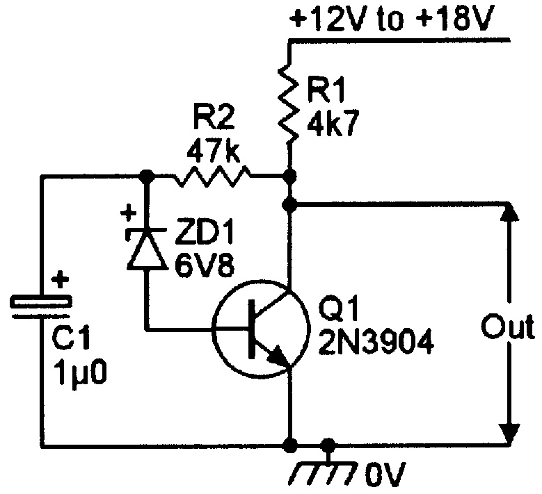
FIGURE 19. Transistor-Zener white noise generator.
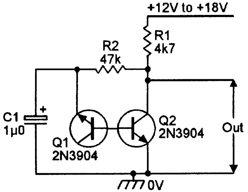
FIGURE 20. Two-transistor white noise generator.
Figure 20 is a simple variation of the above design, with the reverse-biased base-emitter junction of a 2N3904 transistor (which “zeners” at about 6V) used as the noise-generating zener diode. NV