Our first article gave an introductory outline of bipolar transistor principles, characteristics, and basic circuit configurations. This time, we'll concentrate on practical ways of using bipolar transistors in useful common-collector (voltage follower) circuit applications.
COMMON-COLLECTOR AMPLIFIER CIRCUIT
The common-collector amplifier (also known as the grounded-collector amplifier, emitter follower, or voltage follower) can be used in a wide variety of digital and analog amplifier and constant-current generator applications. This month, we start off by looking at practical “digital” amplifier circuits.
DIGITAL AMPLIFIERS
Figure 1 shows a simple NPN common-collector digital amplifier in which the input is either low (at zero volts) or high (at a Vpeak value not greater than the supply rail value). When the input is low, Q1 is cut off and the output is at zero volts. When the input is high, Q1 is driven on and current IL flows in RL, thus generating an output voltage across RL — intrinsic negative feedback makes this output voltage take up a value one base-emitter junction volt-drop (about 600 mV) below the input Vpeak value. Thus, the output voltage “follows” (but is 600 mV less than) the input voltage.
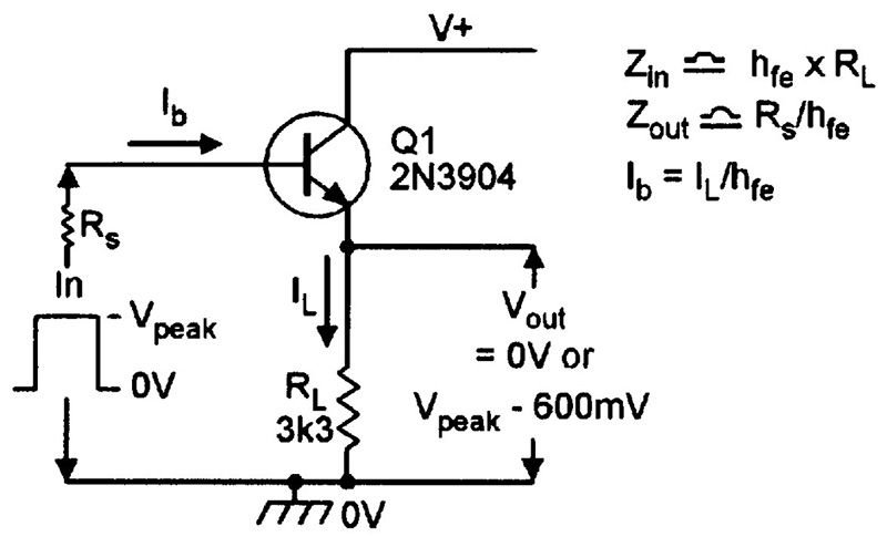
FIGURE 1. Common-collector digital amplifier basic details.
This circuit’s input (base) current equals the IL value divided by Q1’s hfe value (nominally 200 in the 2N3904), and its input impedance equals hfe x RL, i.e., nominally 660K in the example shown. The circuit’s output impedance equals the input signal source impedance (Rs) value divided by hfe. Thus, the circuit has a high input and low output impedance, and acts as a unity-voltage-gain “buffer” circuit.
If this buffer circuit is fed with a fast input pulse, its output may have a deteriorated falling edge, as shown in Figure 2. This deterioration is caused by the presence of stray capacitance (Cs) across RL. When the input pulse switches high, Q1 turns on and rapidly “sources” (feeds) a charge current into Cs, thus giving an output pulse with a sharp leading edge. However, when the input signal switches low again, Q1 switches off and is thus unable to “sink” (absorb) the charge current of Cs, which thus discharges via RL and makes the output pulse’s trailing edge decay exponentially, with a time constant equal to the Cs-RL product.
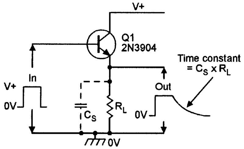
FIGURE 2. Effects of Cs on the circuit’s output pulses in Figure 1.
Note from the above description that an NPN emitter follower can efficiently source (but not sink) high currents — a PNP emitter follower gives the opposite action, and can efficiently sink (but not source) high currents.
RELAY DRIVERS
If the basic Figure 1 switching circuit is used to drive inductive loads such as coils or loudspeakers, etc., it must be fitted with a diode protection network to limit inductive switch-off back-EMFs to safe values. One very useful inductor-driving circuit is the relay driver, and a number of examples of this are shown in Figures 3 to 7.
The relay in the NPN driver circuit in Figure 3 can be activated via a digital input or via switch SW1 — it turns on when the input signal is high or SW1 is closed, and turns off when the input signal is low or SW1 is open.
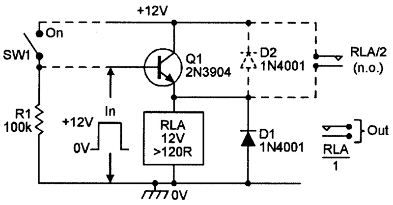
FIGURE 3. Simple emitter-follower relay driver.
Relay contacts RLA/1 are available for external use, and the circuit can be made self-latching by wiring a spare set of normally-open relay contacts (RLA/2) between Q1’s collector and emitter, as shown dotted. Figure 4 is a PNP version of the same circuit; in this case, the relay can be turned on by closing SW1 or by applying a “zero” input signal. Note in Figure 3 that D1 damps relay switch-off back-emfs by preventing this voltage from swinging below the zero-volts rail value. Optional diode D2 can be used to stop this voltage swinging above the positive rail.
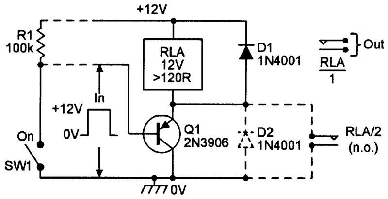
FIGURE 4. PNP version of the relay driver.
The circuits shown in Figures 3 and 4 effectively increase the relay current sensitivity by a factor of about 200 (the hfe value of Q1), e.g., if the relay has a coil resistance of 120R and needs an activating current of 100 mA, the circuit’s input impedance is 24K and the input operating current requirement is 0.5 mA. Sensitivity can be further increased by using a Darlington pair of transistors in place of Q1 (as shown in Figure 5), but the emitter “following” voltage of Q2 will be 1.2V (two base-emitter volt drops) below the base input voltage of Q1.
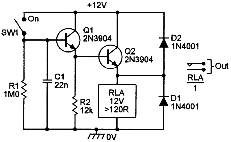
FIGURE 5. Darlington version of the NPN relay driver.
This circuit has an input impedance of 500K and needs an input operating current of 24 µA — C1 protects the circuit against activation via high-impedance transient voltages, such as those induced by lightening flashes, RFI, etc. The Darlington buffer is useful in relay-driving C-R time-delay designs such as those shown in Figures 6 and 7, in which C1-R1 generate an exponential waveform that is fed to the relay via Q1-Q2, thus making the relay change state some delayed time after the supply is initially connected. With an R1 value of 120k, the circuits give operating delays of roughly 0.1 seconds per µF of C1 value, i.e., a 10 second delay if C1 = 100 µF, etc. The Figure 6 circuit makes the relay turn on some delayed time after its power supply is connected. The Figure 7 circuit makes the relay turn on as soon as the supply is connected, but turn off again after a fixed delay.
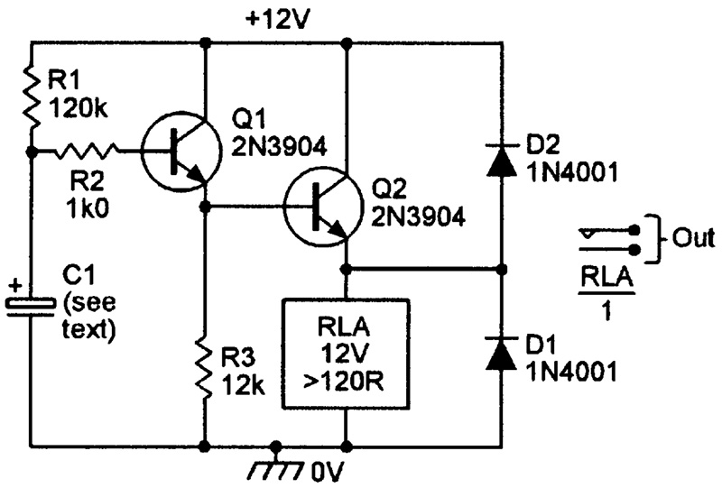
FIGURE 6. Delayed switch-on relay driver.
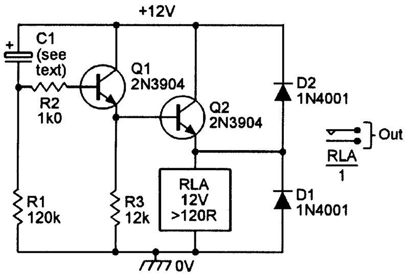
FIGURE 7. Auto-turn-off time-delay circuit.
CONSTANT-CURRENT GENERATORS
A constant-current generator (CCG) is a circuit that generates a constant load current irrespective of wide variations in load resistance. A bipolar transistor can be used as a CCG by using it in the common-collector mode shown in Figure 8. Here, R1-ZD1 applies a fixed 5.6V “reference” to Q1 base, making 5V appear across R2, which thus passes 5mA via Q1’s emitter. A transistor’s emitter and collector currents are inherently almost identical, so a 5mA current also flows in any load connected between Q1’s collector and the positive supply rail, provided that its resistance is not so high that Q1 is driven into saturation.
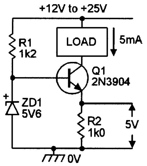
FIGURE 8. Simple 5 mA constant-current generator.
These two points thus act as 5 mA “constant-current” terminals. This circuit’s constant-current value is set by Q1’s base voltage and the R2 value, and can be altered by varying either of these values. Figure 9 shows how the basic circuit can be “inverted” to give a ground-referenced, constant-current output that can be varied from about 1 mA to 10 mA via RV1.
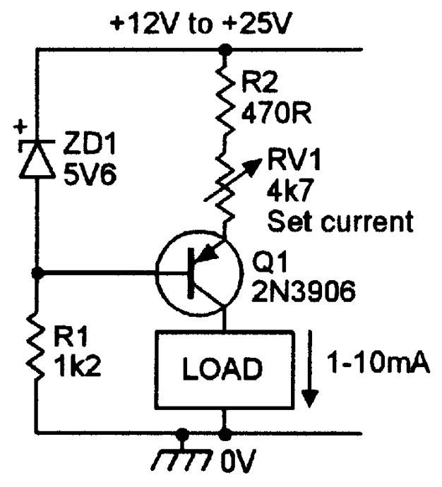
FIGURE 9. Ground-referenced variable (1 mA-10 mA) constant-current generator.
In many practical CCG applications, the circuit’s most important feature is its high dynamic output impedance or “current constancy” — the precise current magnitude being of minor importance — in such cases the basic Figure 8 and 9 circuits can be used. If greater precision is needed, the “reference” voltage accuracy must be improved. One way of doing this is to replace R1 with a 5 mA constant-current generator, as indicated in Figure 10 by the “double circle” symbol, so that the zener current (and thus voltage) is independent of supply voltage variations.
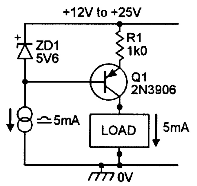
FIGURE 10. Precision constant-current generator.
A red LED acts as an excellent reference voltage generator, and has a very low temperature coefficient, and can be used in place of a zener, as shown in Figure 11.
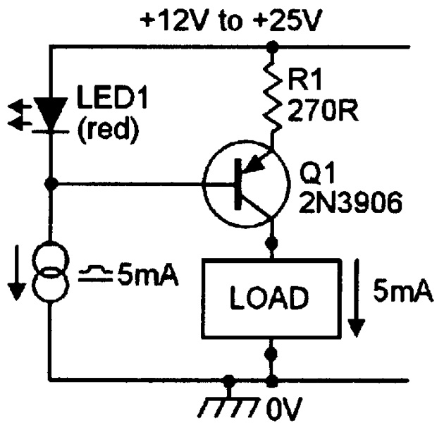
FIGURE 11. Thermally-stabilized constant-current generator, using an LED as a voltage reference.
In this case, the LED generates roughly 2.0V, so only 1.4V appears across R1, which has its value reduced to 270R to give a constant-current output of 5 mA. The CCG (constant-current generator) circuits in Figures 8 through 11 are all “three-terminal” designs that need both supply and output connections. Figure 12 shows a two-terminal CCG that consumes a fixed 2 mA when wired in series with an external load.
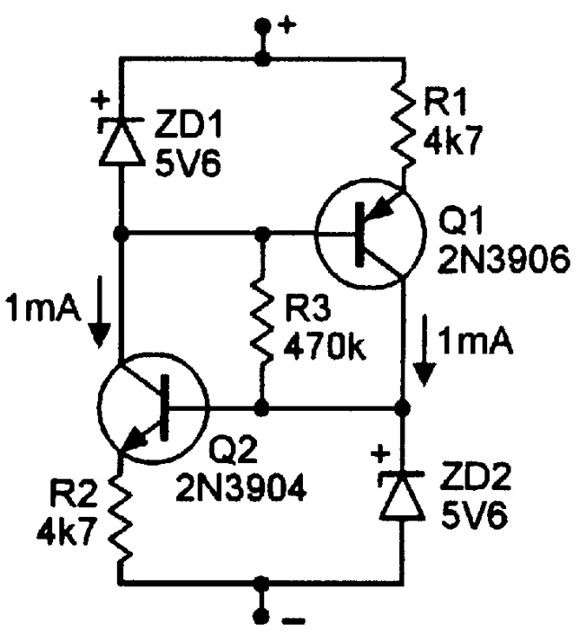
FIGURE 12. Two-terminal 2 mA constant-current generator.
Here, ZD1 applies 5.6V to the base of Q1, which (via R1) generates a constant collector current of 1 mA — this current drives ZD2, which thus develops a very stable 5.6V on the base of Q2 which, in turn, generates a constant collector current of about 1mA, which drives ZD1. The circuit thus acts as a closed-loop current regulator that consumes a total of 2 mA. R3 acts as a start-up resistor that provides the transistor with initial base current. Figure 13 shows a version of the two-terminal CCG in which the operating current is fully variable from 1 mA to 10 mA via dual ganged variable resistor RV1. Note that these two circuits each need a minimum operating voltage, between their two main terminals of about 12V, but can operate with maximum ones of 40V.
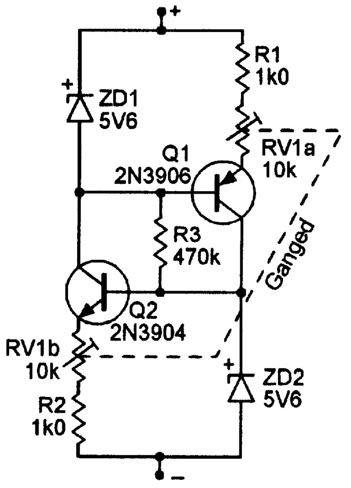
FIGURE 13. Two-terminal variable (1 mA-10 mA) constant-current generator.
LINEAR AMPLIFIERS
A common-collector circuit can be used as an AC-coupled linear amplifier by biasing its base to a quiescent half-supply voltage value (to accommodate maximal signal swings) and AC-coupling the input signal to its base and taking the output signal from its emitter, as shown in the basic circuits in Figures 14 and 15. Figure 14 shows the simplest possible version of the linear emitter follower, with Q1 biased via a single resistor (R1). To achieve half-supply biasing, R1’s value must (ideally) equal Q1’s input resistance — the biasing level is thus dependent on Q1’s hfe value.
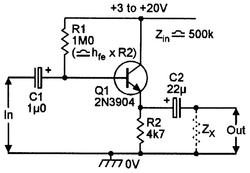
FIGURE 14. Simple emitter follower.
Figure 15 shows an improved version of the basic circuit in which R1-R2 applies a quiescent half-supply voltage to Q1 base, irrespective of variations in Q1’s hfe values. Ideally, R1 should equal the paralleled values or R2 and RIN, but in practice, it is adequate to simply make R1 low relative to RIN, and to make R2 slightly larger than R1.
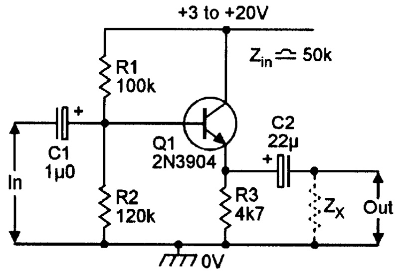
FIGURE 15. High-stability emitter follower.
In these two circuits, the input impedance looking directly into Q1 base equals hfe x Zload, where (in the basic Figure 14 circuit) Zload is the parallel impedance of R2 and external output load ZX. Thus, the base impedance value is roughly 1M0 when ZX is infinite. The input impedance of the complete circuit equals the parallel impedances of the base impedance and the bias network. The circuit in Figure 14 gives an input impedance of about 500K, and the circuit in Figure 15 is about 50K. Both circuits give a voltage gain (AV) that is slightly below unity, the actual gain being given by:
AV = Zload/(Zb + Zload)
where Zb = 25/Ic ohms, and where Ic is the collector current (which is the same as the emitter current) in mA. Thus, at an operating current of 1 mA these circuits give a gain of 0.995 when Zload = 4k7, or 0.975 when Zload = 1k0.
BOOTSTRAPPING
The Figure 15 circuit’s input impedance can easily be boosted by using the basic “bootstrapping” technique shown in Figure 16. Here, 47K resistor R3 is wired between the R1-R2 biasing network junction and Q1 base, and the input signal is fed to Q1 base via C1. Note, however, that Q1’s output is fed back to the R2-R2 junction via C2, and near-identical signal voltages thus appear at both ends of R3 — very little signal current flows in R3, which appears (to the input signal) to have a far greater impedance than its true resistance value.
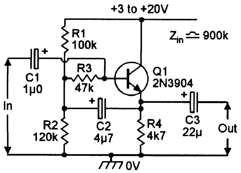
FIGURE 16. Bootstrapped emitter follower.
All practical emitter followers give an AV of less than unity, and this value determines the resistor “amplification factor,” or AR of the circuit, as follows:
AR = 1/(1 - AV)
Thus, if the circuit has an AV or 0.995, AR equals 200 and the R3 impedance is almost 10M. This impedance is in parallel with RIN, so the Figure 16 circuit has an input impedance of roughly 900K. The input impedance of the circuit in Figure 16 can be increased even more by using a pair of Darlington-connected transistors in place of Q1, and increasing the value of R3, as shown in Figure 17, which gives a measured input impedance of about 3M3.
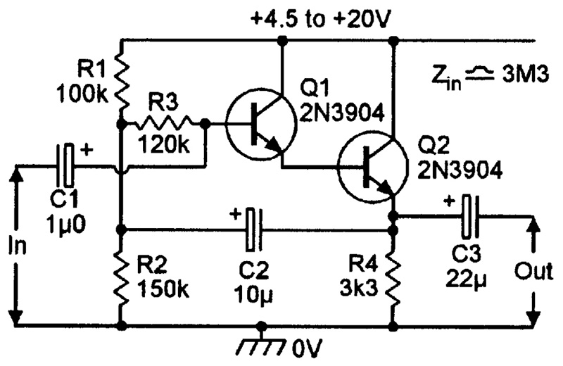
FIGURE 17. Bootstrapped Darlington emitter follower.
An even greater input impedance can be obtained by using the bootstrapped “complementary feedback pair” circuit in Figure 18, which gives an input impedance of about 10M. In this case, Q1 and Q2 are, in fact, both wired as common emitter amplifiers, but they operate with virtually 100 percent negative feedback and give an overall voltage gain of almost exactly unity — this “pair” of transistors thus acts like a near-perfect Darlington emitter follower.
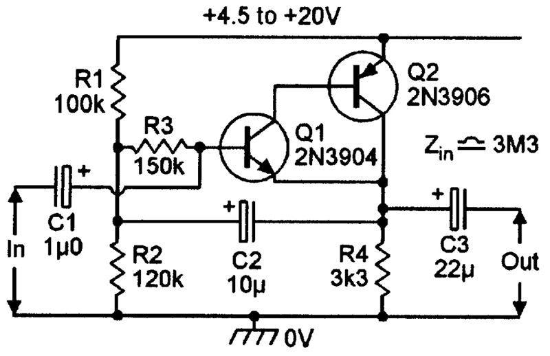
FIGURE 18. Bootstrapped complementary feedback pair.
COMPLEMENTARY EMITTER FOLLOWERS
It was pointed out earlier that an NPN emitter follower can source current, but cannot sink it, and that a PNP emitter follower can sink current, but cannot source it; i.e., these circuits can handle unidirectional output currents only. In many applications, a “bidirectional” emitter follower circuit (that can source and sink currents with equal ease) is required, and this action can be obtained by using a complementary emitter follower configuration in which NPN and PNP emitter followers are effectively wired in series. Figures 19 to 21 show basic circuits of this type.
The circuit in Figure 19 uses a dual (split) power supply and has its output direct-coupled to a grounded load (RL).
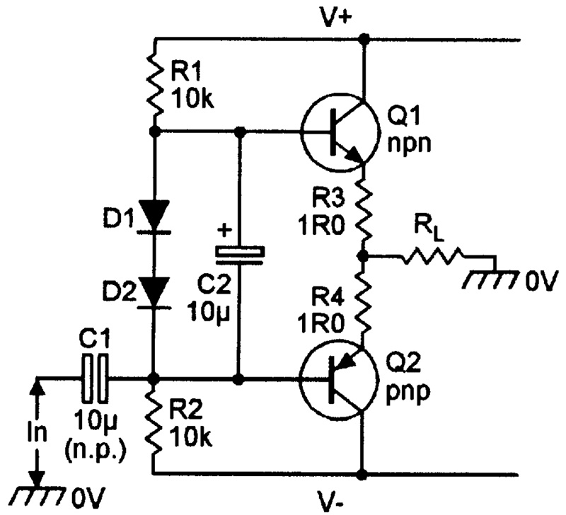
FIGURE 19. Complementary emitter follower using split supply and direct-coupled output load.
The series-connected NPN and PNP transistors are biased at a quiescent “zero volts” value via the R1-D1-D2-R2 potential divider, with each transistor slightly forward-biased via silicon diodes D1 and D2, which have characteristics inherently similar to those of the transistor base-emitter junctions. C2 ensures that identical input signals are applied to the transistor bases, and R3 and R4 protect the transistors against excessive output currents. The circuit’s action is such that Q1 sources current into the load when the input goes positive, and Q2 sinks load current when the input goes negative. Note that input capacitor C1 is a non-polarized type. Figure 20 shows an alternative version of the above circuit, designed for use with a single-ended power supply and an AC-coupled output load — note in this case, that C1 is a polarized type.
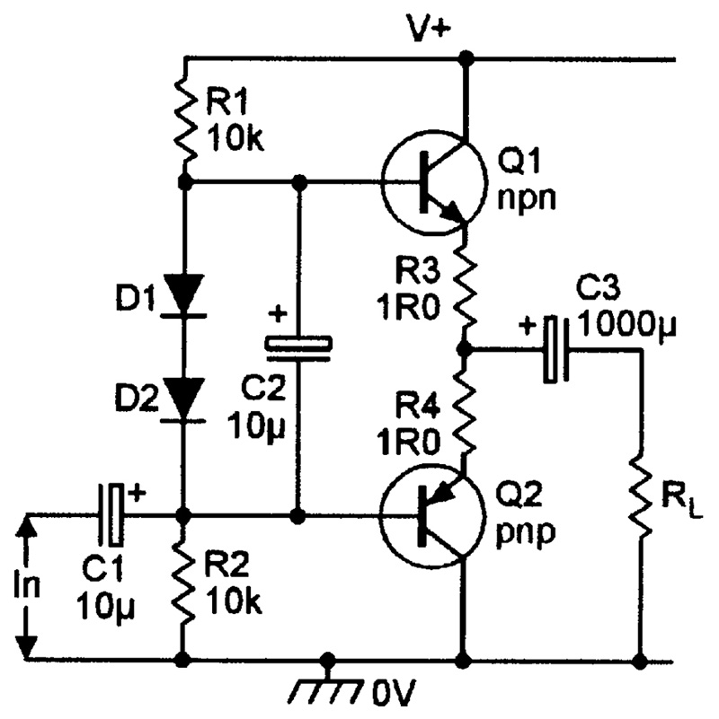
FIGURE 20. Complementary emitter follower using single-ended supply and AC-coupled load.
THE AMPLIFIED DIODE
The Q1 and Q2 circuits in Figures 19 and 20 are slightly forward-biased (to minimize cross-over distortion problems) via silicon diodes D1 and D2 — in practice, the diode currents (and thus the transistor forward-bias voltages) are usually adjustable over a limited range. If these basic circuits are modified for use with Darlington transistors stages, a total of four biasing diodes are needed — in such cases the diodes are usually replaced by a transistor “amplified diode” stage, as shown by the Q5 circuit in Figure 21.
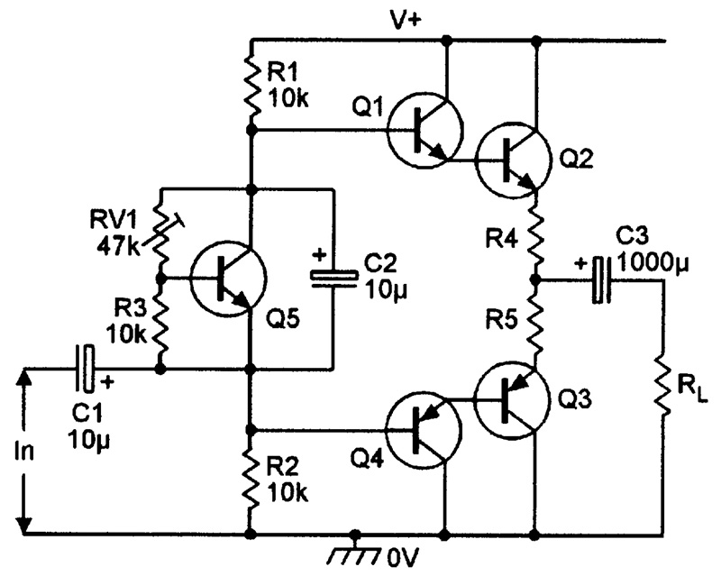
FIGURE 21. Darlington complementary emitter follower, with biasing via an amplified diode (Q5).
In the Figure 21 circuit, Q5’s collector-to-emitter voltage equals the Q5 base-emitter volt drop (about 600 mV) multiplied by (RV1+R3)/R3 — so, if RV1 is set to zero ohms, 600 mV are developed across Q5, which thus acts like a single silicon diode. However, if RV1 is set to 47K, about 3.6V is developed across Q5, which thus acts like six series-connected silicon diodes. RV1 can be used to precisely set the Q5 volt drop and thus adjust the quiescent current values of the Q2-Q3 output stages.
High-power versions of the basic Figure 21 circuit are widely used as the basis of many modern “Hi-Fi” audio power amplifier circuits. Some simple circuits of this type will be described later in this Bipolar Transistor Cookbook series. NV
Part 1 is available here.