The opening piece of this eight-part series described basic transistor principles and configurations (Part 1); subsequent articles went on to describe a wide variety of practical transistor circuits ranging from common-collector amplifiers (Part 2), common-emitter and common-base amplifiers (Part 3), and small-signal audio amplifiers (Part 4), to various practical oscillator (Part 5), multivibrator waveform generator (Part 6), and audio power amplifier (Part 7) circuits. This final episode rounds off the "Transistor Cookbook" subject by presenting a miscellaneous collection of practical and useful transistor circuits and gadgets.
A NOISE LIMITER CIRCUIT
Unwanted electronic "noise" can be a great nuisance; when listening to very weak broadcast signals, for example, peaks of background noise often completely swamp the broadcast signal, making it unintelligible. This problem can often be overcome by using the noise limiter circuit in Figure 1. Here, the signal-plus-noise waveform is fed to amplifier Q1 via RV1. Q1 amplifies both waveforms equally, but D1 and D2 automatically limit the peak-to-peak output swing of Q1 to about 1.2 V. Thus, if RV1 is adjusted so that the signal output is amplified to this peak level, the noise peaks will not be able to greatly exceed the signal output, and intelligibility is greatly improved.
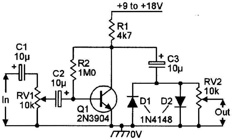
FIGURE 1. Noise limiter.
ASTABLE MULTIVIBRATOR CIRCUITS
The astable multivibrator circuit has many practical uses. It can be used to generate a non-symmetrical 800 Hz waveform that produces a monotone audio signal in the loudspeaker when S1 is closed (Figure 2). The circuit can be used as a Morse code practice oscillator by using a Morse key as S1; the tone frequency can be changed by altering the C1 and/or C2 values.
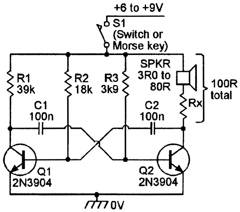
FIGURE 2. Morse code practice oscillator.
Figure 3 shows an astable multivibrator used as the basis of a "signal injector-tracer" item of test gear. When SW1 is in INJECT position 1, Q1 and Q2 are configured as a 1 kHz astable, and feed a good square wave into the probe terminal via R1-C1. This waveform is rich in harmonics, so if it is injected into any AF or RF stage of an AM radio, it produces an audible output via the radio's loudspeaker, unless one of the radio's stages is faulty. By choosing a suitable injection point, the injector can be used to trouble-shoot a defective radio.
FIGURE 3. Signal injector-tracer.
When SW1 is switched to TRACE position 2, the Figure 3 circuit is configured as a cascaded pair of common-emitter amplifiers, with the probe input feeding to Q1 base, and Q2 output feeding into an earpiece or head-set. Any weak audio signals fed to the probe are directly amplified and heard in the earpiece, and any amplitude-modulated RF signals fed to the probe are demodulated by the non-linear action of Q1. The resulting audio signals are then amplified and heard in the earpiece. By connecting the probe to suitable points in a radio, the tracer can thus be used to trouble-shoot a faulty radio, etc.
LIE DETECTOR
The lie detector of Figure 4 is an experimenter's circuit, in which the victim is connected (via a pair of metal probes) into a Wheatstone bridge, formed by R1-RV1-Q1 and R3-R4; the 1 mA center-zero meter is used as a bridge-balance detector. In use, the victim makes firm contact with the probes and, once he/she has attained a relaxed state (in which the skin resistance reaches a stable value), RV1 is adjusted to set a null on the meter. The victim is then cross-questioned and, according to theory, the victim's skin resistance will then change, causing the bridge to go out of balance if he/she lies or shows any sign of emotional upset (embarrassment, etc.) when being questioned.
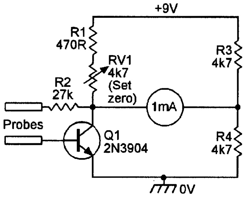
FIGURE 4. Simple lie detector.
CURRENT MIRRORS
A current mirror is a constant-current generator in which the output current magnitude is virtually identical to that of an independent input control current. This type of circuit is widely used in modern linear IC design. Figure 5 shows a simple current mirror using ordinary npn transistors; Q1 and Q2 are a matched pair and share a common thermal environment.
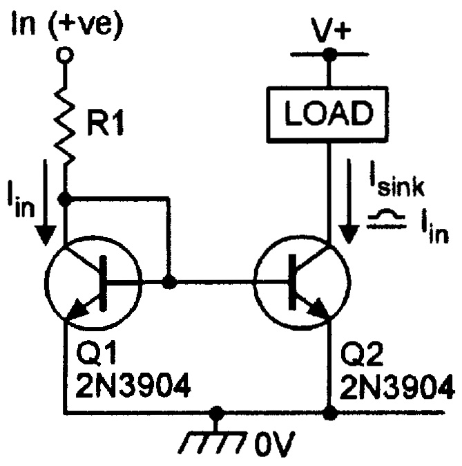
FIGURE 5. An npn current mirror.
When input current Iin is fed into diode-connected Q1, it generates a proportionate forward base-emitter voltage, which is applied directly to the base-emitter junction of matched transistor Q2, causing it to sink an almost identical (mirror) value of collector current, Isink. Q2 thus acts as a constant current sink that is controlled by Iin, even at collector voltages as low as a few hundred millivolts.
Figure 6 shows a pnp version of the simple current mirror circuit. This works in the same basic way as already described, except that Q2's collector acts as a constant current source that has its amplitude controlled by Iin. Note that both of these circuits still work quite well as current-controlled, constant-current sinks or sources, even if Q1 and Q2 have badly matched characteristics, but in this case may not act as true current mirrors, since their Isink and Iin values may be very different.
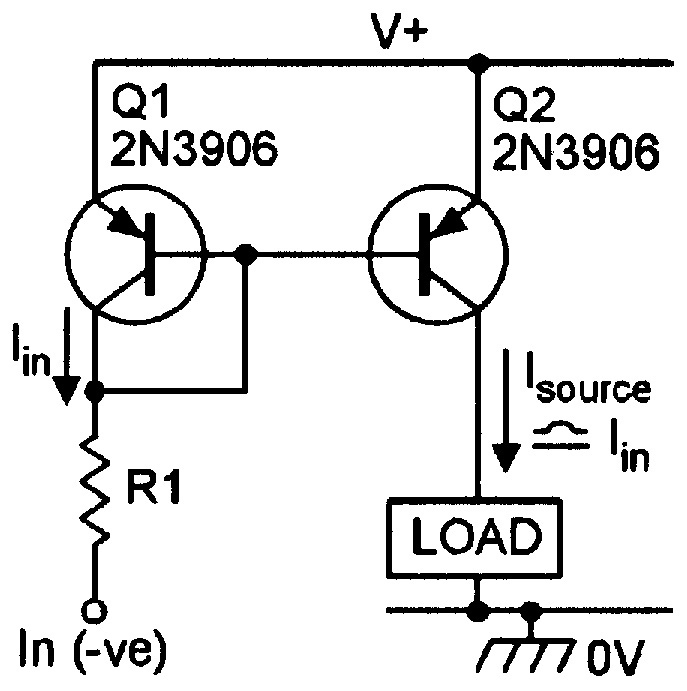
FIGURE 6. A pnp current mirror.
AN ADJUSTABLE ZENER
Figure 7 shows the circuit of an adjustable zener that can have its output voltage pre-set over the range 6.8 V to 21 V via RV1. The circuit action is such that a fixed reference voltage (equal to the sum of the zener and Vbe values) is generated between Q1's base and ground (because of the value of zener voltage used) and has a near-zero temperature coefficient. The circuit's output voltage is equal to Vref multiplied by (RV1 + R1)/R1, and is thus pre-settable via RV1. This circuit is used like an ordinary zener diode, with the RS value chosen to set its operating current at a nominal value in the range 5 to 20 mA.
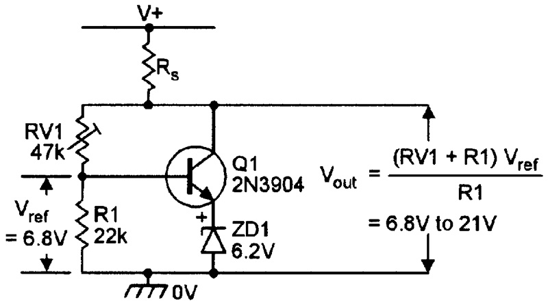
FIGURE 7. Adjustable zener.
L-C OSCILLATORS
L-C oscillators have many applications in test gear and gadgets, etc. Figure 8 shows an L-C medium-wave (MW) signal generator or beat-frequency oscillator (BFO), with Q1 wired as a Hartley oscillator that uses a modified 465 kHz IF transformer as its collector load. The IF transformer's internal tuning capacitor is removed, and variable oscillator tuning is available via VC1, which enables the output frequency (on either fundamentals or harmonics) to be varied from well below 465 kHz to well above 1.7 MHz. Any MW radio will detect the oscillation frequency if placed near the circuit; if the unit is tuned to the radio's IF value, a beat note will be heard, enabling CW and SSB transmissions to be clearly heard.
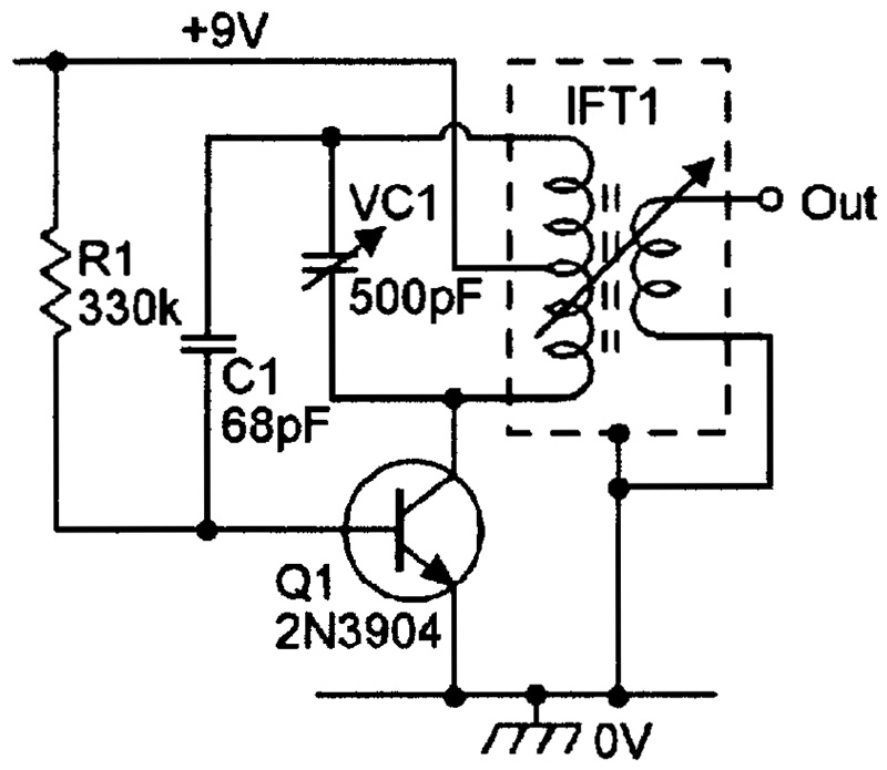
FIGURE 8. MW signal generator/BFO.
Figure 9 shows the above oscillator modified so that, when used in conjunction with a MW radio, it functions as a simple metal/pipe locator. Oscillator coil L1 is hand-wound and comprises 30 center-tapped turns of wire, firmly wound over about a 25 mm (one-inch) length of a 75 to 100 mm (three- to four-inch) diameter non-metallic former or search head and connected to the main circuit via a three-core cable. The search head can be fixed to the end of a long non-metallic handle if the circuit is to be used in the classic metal detector mode, or can be hand-held if used to locate metal pipes or wiring hidden behind plasterwork, etc. Circuit operation relies on the fact that L1's electromagnetic field is disturbed by the presence of metal, causing the inductance of L1 and the frequency of the oscillator to alter. This frequency shift can be detected on a portable MW radio placed near L1 by tuning the radio to a local station and then adjusting VC1 so that a low frequency beat or whistle note is heard from the radio. This beat note changes if L1 (the search head) is placed near metal.
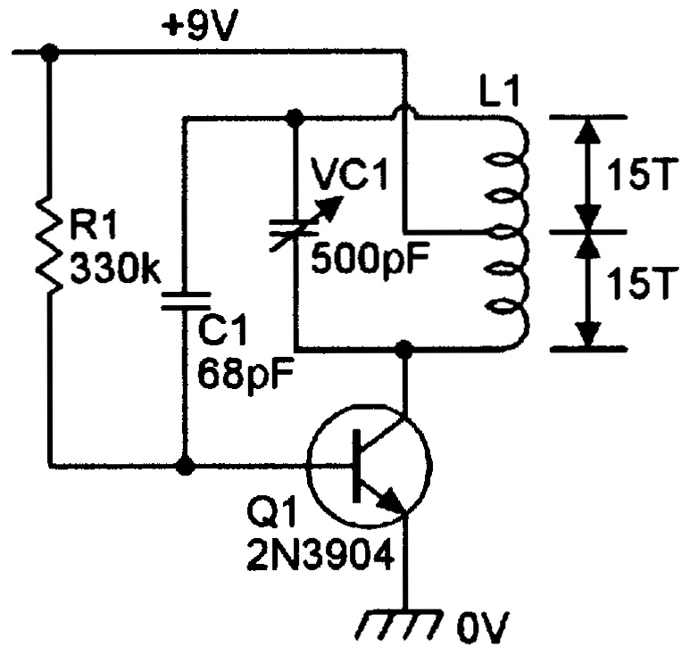
FIGURE 9. Metal/pipe locator.
Figure 10 shows another application of the Hartley oscillator. In this case, the circuit functions as a DC-to-DC converter, which converts a 9 V battery supply into a 300-V DC output. T1 is a 9V-0-9V to 250 V transformer, with its primary forming the L part of the oscillator. The supply voltage is stepped up to about 350 V peak at T1 secondary, and is half-wave rectified by D1 and used to charge C3. With no permanent load on C3, the capacitor can deliver a powerful but non-lethal belt. With a permanent load on the output, the output falls to about 300 V at a load current of a few mA.
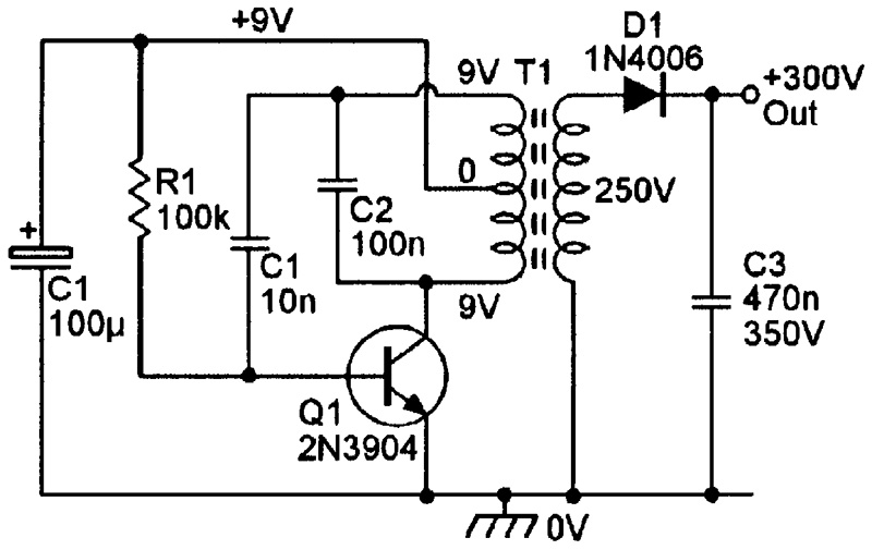
FIGURE 10. 9 V to 300 V DC-to-DC converter.
FM TRANSMITTERS
Figures 11 and 12 show a pair of low-power FM transmitters that generate signals that can be picked up at a respectable range on any 88 to 108 MHz FM-band receiver. The Figure 11 circuit uses IC1 as a 1 kHz squarewave generator that modulates the Q1 VHF oscillator, and produces a harsh 1 kHz tone signal in the receiver; this circuit thus acts as a simple alarm-signal transmitter.
FIGURE 11. FM radio transmitter alarm.
The Figure 12 circuit uses a two-wire electret microphone insert to pick up voice sounds, etc., which are amplified by Q1 and used to modulate the Q2 VHF oscillator; this circuit thus acts as an FM microphone or bug. In both circuits, the VHF oscillator is a Colpitts type, but with the transistor used in the common-base mode and C7 giving feedback from the tank output back to the emitter input.
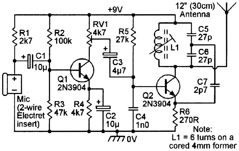
FIGURE 12. FM microphone/bug transmitter.
These two circuits have been designed to conform to American FCC regulations, and they thus produce a radiated field strength of less than 50 µV/m at a range of 15 meters (15 yards), and can be freely used in the USA. It should be noted, however, that their use is quite illegal in many countries, including the UK.
To set up these circuits, set the coil slug at its middle position, connect the battery, and tune the FM receiver to locate the transmitter frequency. If necessary, trim the slug to tune the transmitter to a clear spot in the FM band. RV1 should then be trimmed to set the modulation at a clean level.
TRANSISTOR AC VOLTMETERS
An ordinary moving-coil meter can be made to read AC voltages by feeding them to it via a rectifier and suitable multiplier resistor, but produces grossly non-linear scale readings if used to give FSD values below a few volts. This non-linearity problem can be overcome by connecting the meter circuitry into the feedback loop of a transistor common-emitter amplifier, as shown in the circuits of Figures 13 to 15, which (with the Rm values shown) each read 1 V FSD.
The Figure 13 circuit uses a bridge rectifier type of meter network, and draws a quiescent current of 0.3 mA, has an FSD frequency response that is flat from below 15 Hz to above 150 kHz, and has superb linearity up to 100 kHz when using IN4148 silicon diodes or to above 150 kHz when using BAT85 Schottky types. R1 sets Q1's quiescent current at about treble the meter's FSD value, and thus gives the meter automatic overload protection.
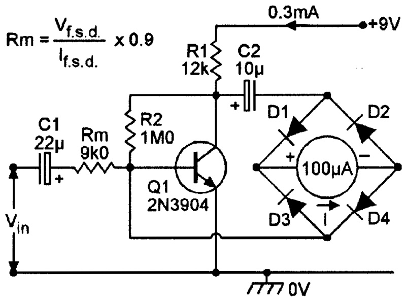
FIGURE 13. The frequency response of this 1 V AC meter is flat to above 150 kHz.
Figures 14 and 15 show pseudo full-wave and ghosted half-wave versions of the above circuit. These have a performance similar to that of Figure 13, but with better linearity and lower sensitivity. D3 is sometimes used in these circuits to apply slight forward bias to D1 and D2 and thus enhance linearity, but this makes the meter pass a standing current when no AC input is applied. The diodes used in these and all other electronic AC meter circuits shown in this article should be either silicon (IN4148, etc.) or (for exceptionally good performance) Schottky types; germanium types should not be used.
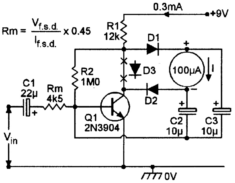
FIGURE 14. Pseudo full-wave version of the 1 V AC meter.
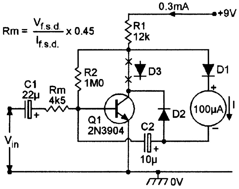
FIGURE 15. Ghosted half-wave version of the 1 V AC meter.
In the circuits in Figures 13 to 15, the FSD sensitivity is set at 1 V via Rm, which can not be reduced below the values shown without incurring a loss of meter linearity.
The Rm value can, however, safely be increased, to give higher FSD values, e.g., by a factor of 10 for 10 V FSD, etc.
If greater FSD sensitivity is wanted from the above circuits, it can be obtained by applying the input signal via a suitable pre-amplifier, i.e., via a +60 dB amplifier for 1 mV sensitivity, etc. Figure 16 shows this technique applied to the Figure 13 circuit, to give an FSD sensitivity variable between 20 mV and 200 mV via RV1. With the sensitivity set at 100 mV FSD, this circuit has an input impedance of 25 K and a bandwidth that is flat within 0.5 dB to 150 kHz.
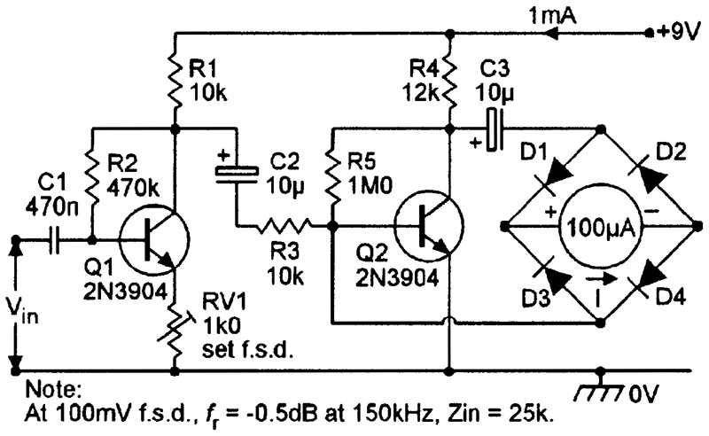
FIGURE 16. This AC voltmeter can be set to give FSD sensitivities in the range 20 mV to 200 mV.
AC MILLIVOLTMETER CIRCUITS
A one-transistor AC meter cannot be given an FSD sensitivity greater than 1 V without loss of linearity. If greater sensitivity is needed, two or more stages of transistor amplification must be used. The highest useful FSD sensitivity that can be obtained (with good linearity and gain stability) from a two-transistor circuit is 10 mV, and Figure 17 shows an excellent example that gives FSD sensitivities in the range 10 mV to 100 mV (set via Rx). It uses D1 and D2 in the "ghosted half-wave" configuration, and its response is flat within 0.5 dB to above 150 kHz; the circuit's input impedance is about 120 K when set to give 100 mV FSD sensitivity (Rx = 470 Ohms); when set to give 10 mV sensitivity (Rx = 47 Ohms), the input impedance varies from 90 K at 15 kHz to 56 K at 150 kHz.
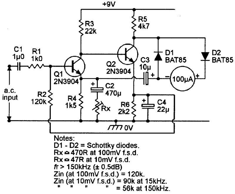
FIGURE 17. Wideband AC millivoltmeter with FSD sensitivity variable from 10 mV to 100 mV via Rx.
Figure 18 shows a simple x10 pre-amplifier that can be used to boost the above circuit's FSD sensitivity to 1 mV; this circuit has an input impedance of 45 K and has a good wideband response. Note, when building highly sensitive AC millivoltmeters, great care must be taken to keep all connecting leads short, to prevent unwanted RF pickup.
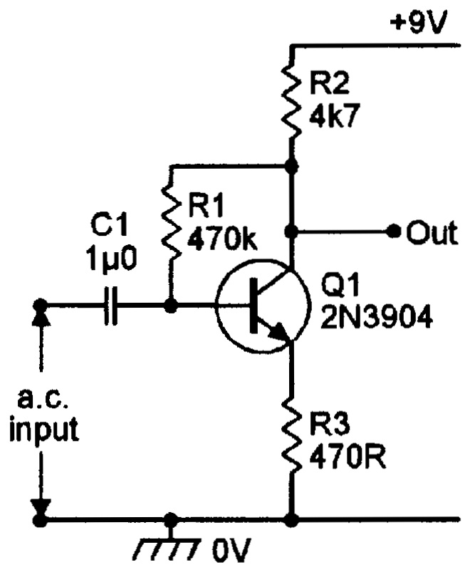
FIGURE 18. This x10 wideband pre-amplifier is used to boost an AC millivoltmeter's sensitivity.
A wide-range AC volt/millivolt meter can be made by feeding the input signals to a sensitive AC meter via suitable attenuator circuitry. To avoid excessive attenuator complexity, the technique of Figure 19 is often adopted; the input is fed to a high-impedance unity-gain buffer, either directly (on "mV" ranges) or via a compensated 60 dB attenuator (on V ranges), and the buffer's output is fed to a basic 1 mV FSD meter via a simple low-impedance attenuator, which in this example has 1-3-10, etc., ranging.
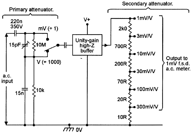
FIGURE 19. Basic multi-range AC volt/millivolt meter circuit.
Note, when using this circuit that its input-to-unity-gain-buffer-output frequency response is virtually flat over the (typical) frequency range 20 Hz-150 kHz when used on the "mV" ranges, and that the primary attenuator's 15 pF trimmer must — when initially setting up the circuit — be adjusted on test to obtain the same frequency response on the basic "V" range.
Figure 20 shows a useful variation of the above technique. In this case, the input buffer also serves as a x10 amplifier, and the secondary attenuator's output is fed to a meter with 10 mV FSD sensitivity, the net effect being that a maximum overall sensitivity of 1 mV is obtained with a minimum of complexity.
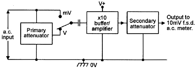
FIGURE 20. A useful AC volt/millivolt meter circuit variation.
Figures 21 and 22 show input buffers suitable for use with the above types of multi-range circuits. The Figure 21 design is that of a unity-gain buffer; it gives an input impedance of about 4.0 M.
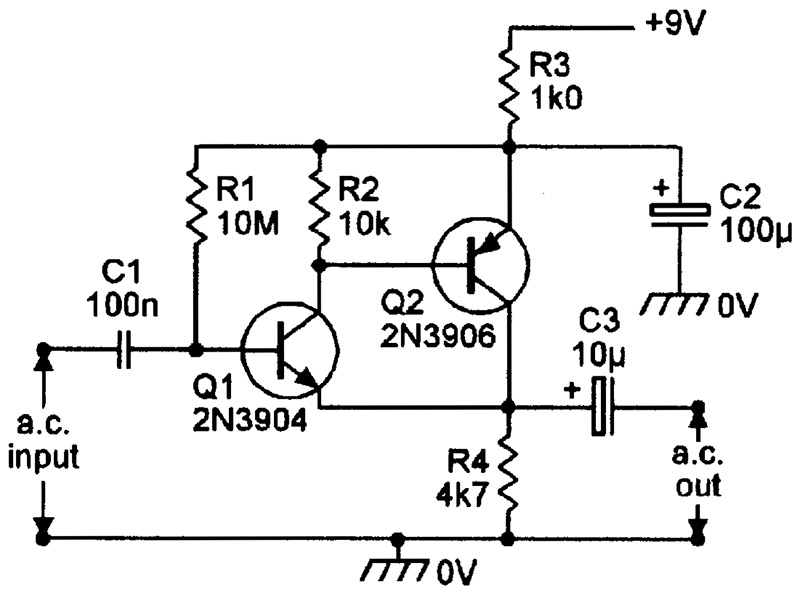
FIGURE 21. Unity-gain input buffer.
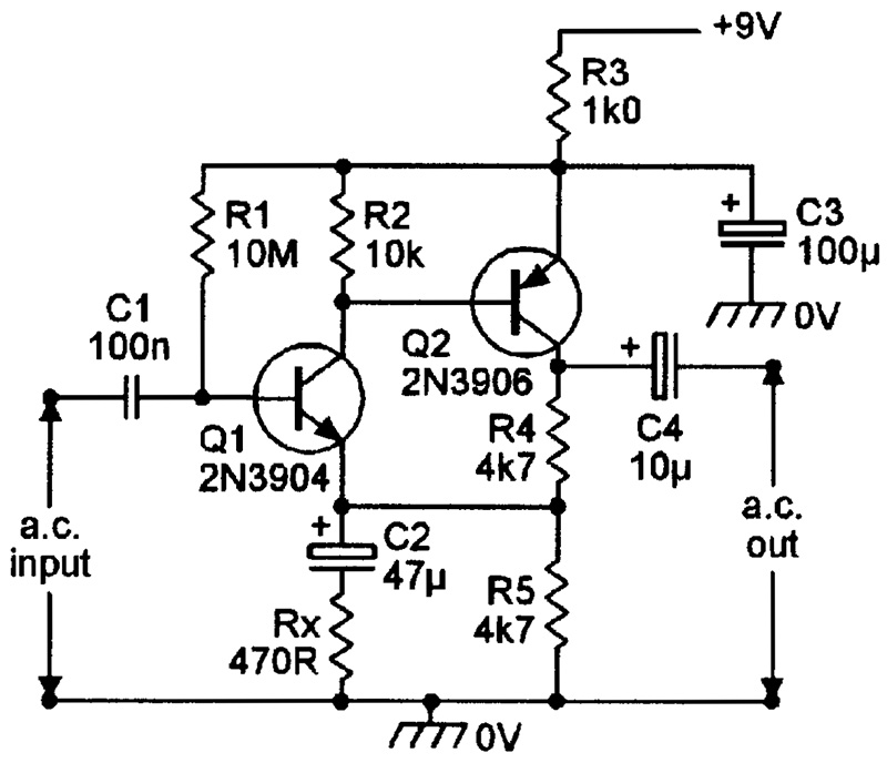
FIGURE 22. Buffer with x10 gain.
The Figure 22 buffer gives a x10 voltage gain (set by the R1/Rx ratio) and has an input impedance of 1.0 M. NV