(Lead Photo above) The final two-line LED sign and controller with a red plastic filter that enhances contrast. The controller board drives each row of LEDs and sends bit patterns to each row in sequence.
When you plan to create a large sign with LED dot-matrix modules, the circuits and software can seem like a big challenge. However, the step-by-step approach in this tutorial gives you what you need to know to make a sign of your own.
I bought a used LED sign from a local electronics store and took it apart. It contained two rows of 14 large 5x7 LED modules. The display lit up with messages from an old arcade game, but I couldn’t figure out how to get it to display new information.
With the help of a logic analyzer, I determined how the controller worked and decided to keep the display board, then scrap the controller and create my own.
I’ll explain how to do it, and you’ll have a complete dot-matrix sign-control circuit and software along with PCB (printed circuit board) layouts and plain-text code. You can control 5x7 or 8x8 LED modules (see Note 1).
In this article, you will learn how:
- FETs and shift registers control LEDs in a sign.
- An MCU (microcontroller) stores and uses bit patterns to represent letters, numbers, and punctuation marks.
- C code addresses the proper rows of bits in an EEPROM to get and display characters.
- A programmable system on a chip simplifies controller hardware and software.
A Cathode and Anode Refresher
To start, look at a 5x7 LED module that provides a matrix of LEDs (Figure 1). The LEDs for our project require common-anode connection for the rows and common-cathode connections for the columns. To turn on LEDs in a row, we apply current to that row’s anode pin and sink current through the cathode pins for the corresponding LEDs we want to turn on. That gives us an easy way to control LEDs a row at a time, and that’s how the controller will work.
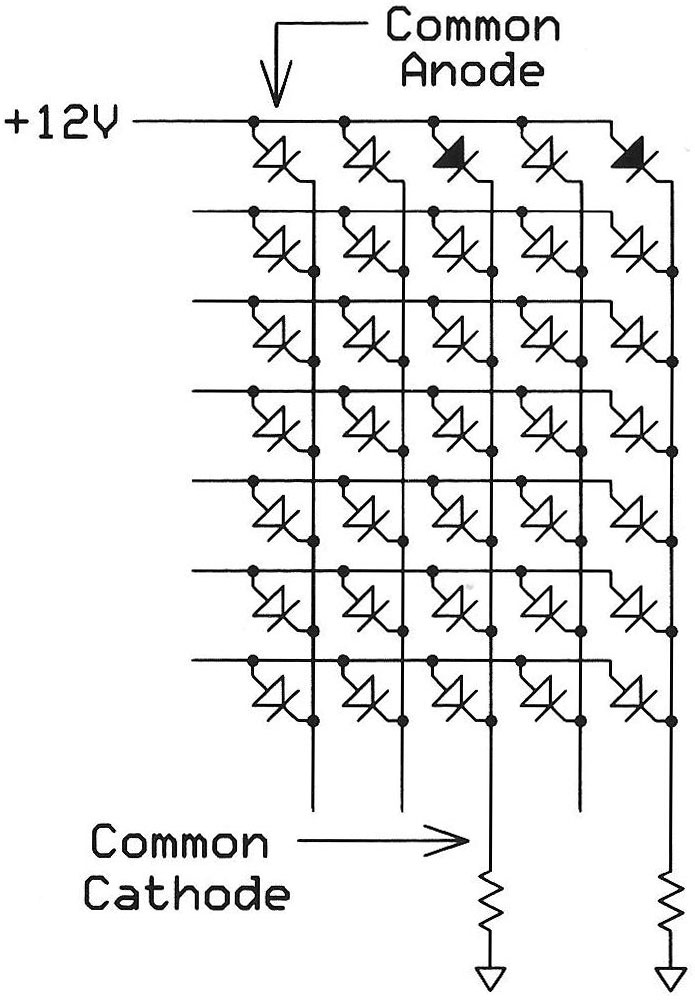
FIGURE 1. A 5x7 LED matrix with common-anode rows and common-cathode columns. A circuit supplies current for a row at a time and ground connections, or current sinks, determine which LEDs turn on for each row.
A commercial controller illuminates LEDs in one row at a time, but quickly enough so our eyes don’t see any flicker as one row turns off and the next row turns on. Figure 2 shows the sequence of illuminated rows for the letter B.
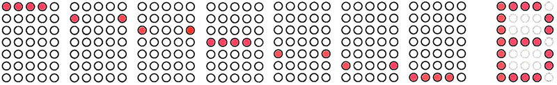
FIGURE 2. When a controller rapidly turns on LEDs in one row at a time, this sequence appears to our eyes as the letter B.
In a horizontal line of LED modules, the common-anode pin for a given row of LEDs connects to the same common-anode pin on all other LED modules. This arrangement means we supply current to only seven or eight LED rows, one at a time. However, each LED column — all 70 in my sign — needs its own on-off circuit to let current flow to ground so we can select individual LEDs. My design supplies +12V to the LED rows.
Drive Rows, Sink Columns, Shift Bits
We must figure out how to electronically drive current through a sign’s LEDs. I had many IRF9520 power MOSFETs on hand and used eight of them; one per row. I/O pins on 3.3V or 5V MCUs can’t handle a 12 volt MOSFET gate-control voltage, so I chose a ULN2803A Darlington-transistor array as an interface between my MCU’s I/O pins and the MOSFET gates (Figure 3).
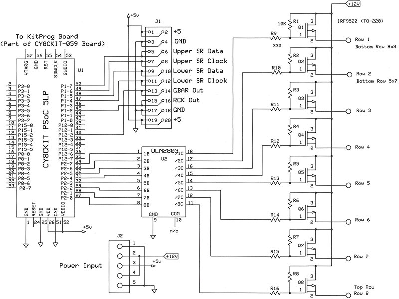
FIGURE 3. Circuit diagram of the eight FETs and a ULN2803A that supply current to the seven or eight rows of LEDs in a single-line display.
Next, we need circuits to sink current from the common-cathode pins for LED columns. Because the controller turns on LEDs row by row, the current-sink circuits will carry only the current for a single LED. My sign needed 70 current sinks, but few MCUs we can reasonably work with have 70 or more I/O pins, so my controller circuit uses eight-bit shift registers connected in series.
Nine eight-bit shift registers give me 72 current sinks. You can add or remove shift registers to suit your requirements. The shift registers receive bit patterns for a given row of LEDs via a serial I/O pin. The MCU’s software governs the shift rate via a shift-clock signal.
Figure 4 shows the general timing between two row-control signals and the transmission of serial data to a shift register.
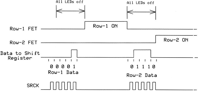
FIGURE 4. A simplified timing diagram for two rows of LEDs in a single 5x7 LED module. Note the LED “off” time between the row 1 and row 2 “on” periods.
In this example, the controller turns off the LEDs as it shifts out new bits for a row. It then turns the LEDs on for that row. This approach causes LEDs to flicker as rows turn on and off. We avoid this problem with an eight-bit shift register such as the 74LS595 that includes an output latch (Figure 5).
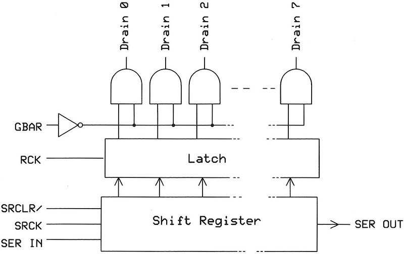
FIGURE 5. Block diagram for a 74LS595 shift register with a latch output.
A 74LS595 shift register receives serial bits from an MCU at its SER IN pin. If it receives more than eight, it passes them on to another shift register — if any — via its SER OUT pin. Pulses on the serial-clock signal, SRCK, transfer a bit at a time into the shift register. However, the shift register’s bits do not transfer into the latch until a control circuit asserts the RCK input. So, an MCU can load the shift register with a new row of bits at the same time the latch sinks current from the lit LEDs for the previous row.
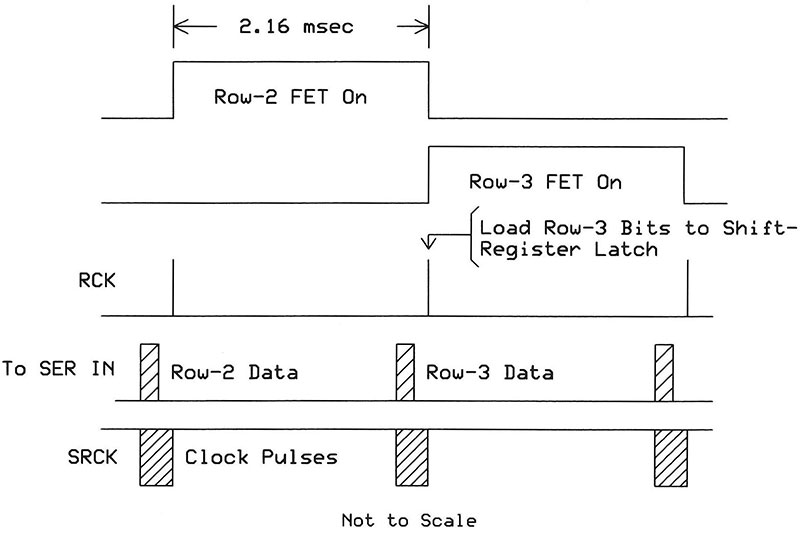
FIGURE 6. Timing diagram for a sign with shift registers that include latched outputs. The filler bits turn off LEDs not used at the end of a message. The SRCK signal goes to all shift-register ICs.
Think of loading the shift register as a “background” operation that doesn’t interfere with the state of the LEDs, thus no flicker. Figure 6 illustrates the timing for two LED rows, and Figure 7 enlarges the bit-shift, SRCK, and SER OUT signals, and the latch-transfer signal, RCK.
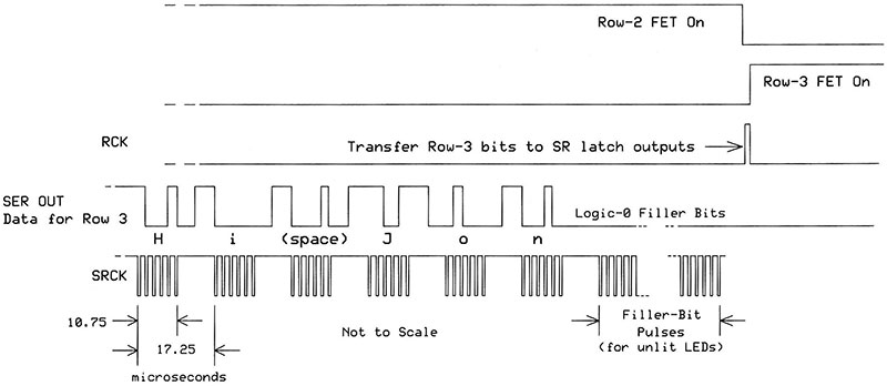
FIGURE 7. An expanded view of the signals that control a sign’s shift registers and FET control signals.
Unfortunately, 74LS595 ICs cannot withstand the +12V I use to drive the LED rows, but a similar shift register (the TPIC6B595) can. Its latch outputs will sink a 150 mA current and handle a 50V load, which makes it an ideal current sink for LED columns. These shift registers come in 20-pin DIP or 20-pin SOIC package types (see Note 2).
The TPIC6B595 includes a GBAR signal that enables the latch outputs. My circuit uses the GBAR signal, but you could just connect it to ground (logic 0).
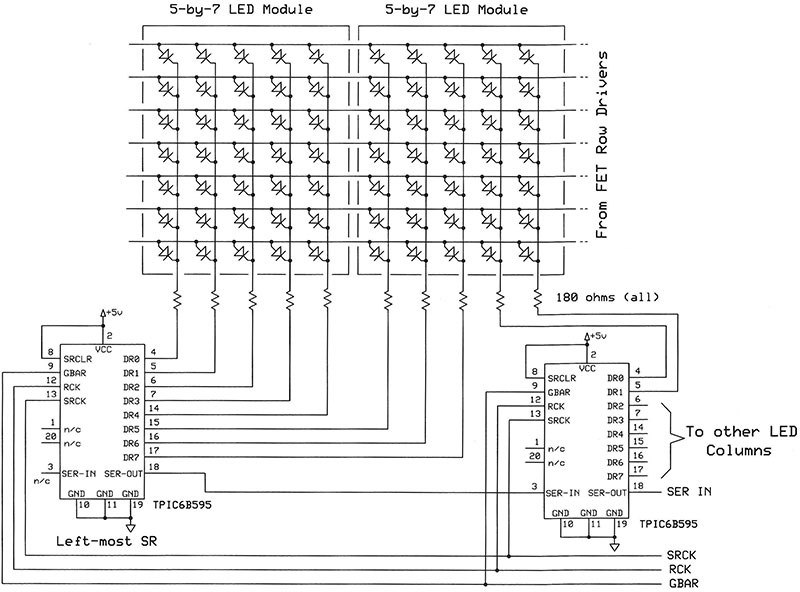
FIGURE 8. Circuit diagram for two of several TPIC6B595 shift registers that sink current from 5x7 LED modules. Each column requires a current-limiting resistor.
Figure 8 shows a shift-register circuit for two of the 5x7 modules on my sign board, and Figure 9 illustrates a similar circuit for an 8x8 LED module.
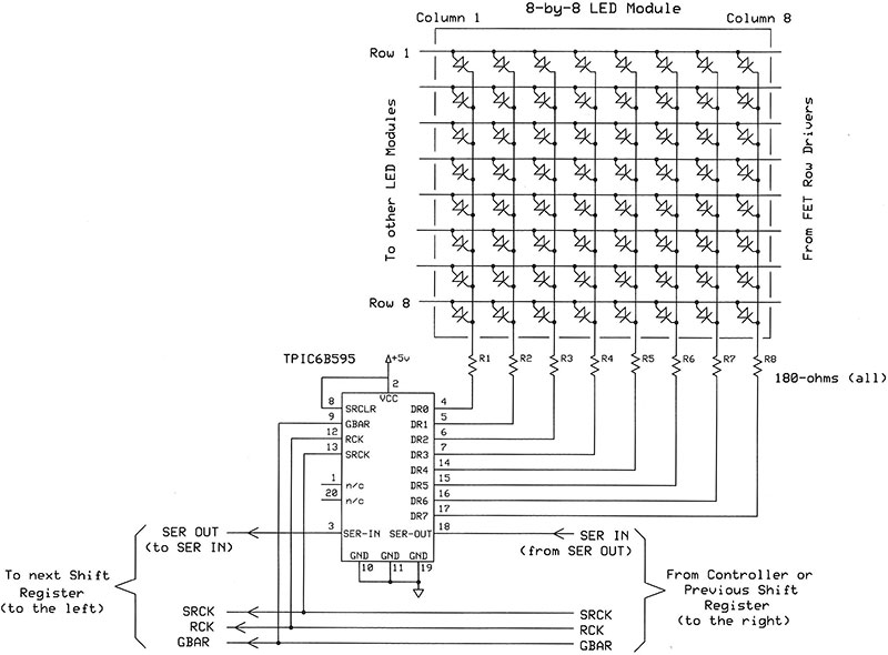
FIGURE 9. Circuit diagram for one TPIC6B595 shift register that sinks current from an 8x8 LED module.
To create a new sign, I recommend 8x8 LED modules because you can put one on a board with its own TPIC6B595 shift register and eight resistors. Then, you connect these modules in series to create a line of displays.
Caution: Sellers of 8x8 LED matrices might specify them only as “common cathode” or “common anode.” In an LED matrix, you’ll always have common cathodes and common anodes! To work with my controller circuitry, you want common-anodes on the rows and common-cathodes on the columns.
Get the Dots, Form a Letter
So far, so good, but where do the bits come from to create alphanumeric characters and symbols? (For clarity, I’ll refer to all of these as “characters.”) Years ago, displays used a read-only memory (ROM) preloaded with the 1s and 0s that form characters. A character-generator ROM held patterns for the 96 “printable” ASCII characters and 32 extra characters such as arrows, checkmarks, and other symbols, for a total of 128 characters (see Resources).
Each of those characters needed eight bytes to store its pattern of 1s and 0s, so the ROM required 1024 bytes (128 x 8). That meant the ROM needed 10 address lines (1024 = 210). Although the ROM used only seven bytes per character, it’s easier to step through binary row addresses eight at a time.
The 10 address lines, A9-A0, separate into a “high” address, A9-A3, and into a “low” address, A2-A0. The high address identifies a specific character; for example, A, f, $, and so on. The low address identifies one of the character’s eight rows (Figure 10).
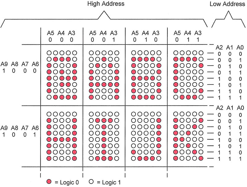
FIGURE 10. A portion of a character-generator ROM shows how high-address bits A9-A3 locate a character and low-address bits A2-A0 indicate a row of bits for that character.
The high address 10000012 (0x41), for example, locates the letter A and the high address 10010112 (0x4B) locates the letter K. These addresses are the same as the seven-bit ASCII codes that print A and K. Now, take into account the three low address bits and we have a 10-bit address such as 1000010 0012 (intentional spacing) that points to the top row of bits for the letter B. Or, consider 1000011 1112 that points to the bottom row of bits for C. (We always ignore the bytes at low address 0002.) The ROM would put out the corresponding five bits that get sent serially to the column shift registers.
A short program in the downloads for this article loads the bit patterns into an MCU’s EEPROM for you. Use the program’s code and character bytes as you wish.
Set Up the Electronics
You can choose any MCU that includes sufficient I/O ports, an SPI port, and at least 1024 bytes of on-chip EEPROM for character-pattern storage. I chose a Cypress Semiconductor CY8C5888LTI-LP097 programmable system-on-a-chip (PSoC) for the controller MCU. This device incorporates an ARM Cortex-M3 processor and it lets developers “create” hardware functions, or blocks, on the chip as they need them. The PSoC’s 2 KB of EEPROM easily stores character bit patterns and leaves room for custom symbols you might add. A CY8CKIT-059 board which includes the PSoC IC costs $10 and the PSoC Creator software is available as a free download (see Note 3). You also need the free PSoC Creator software; more about that soon.
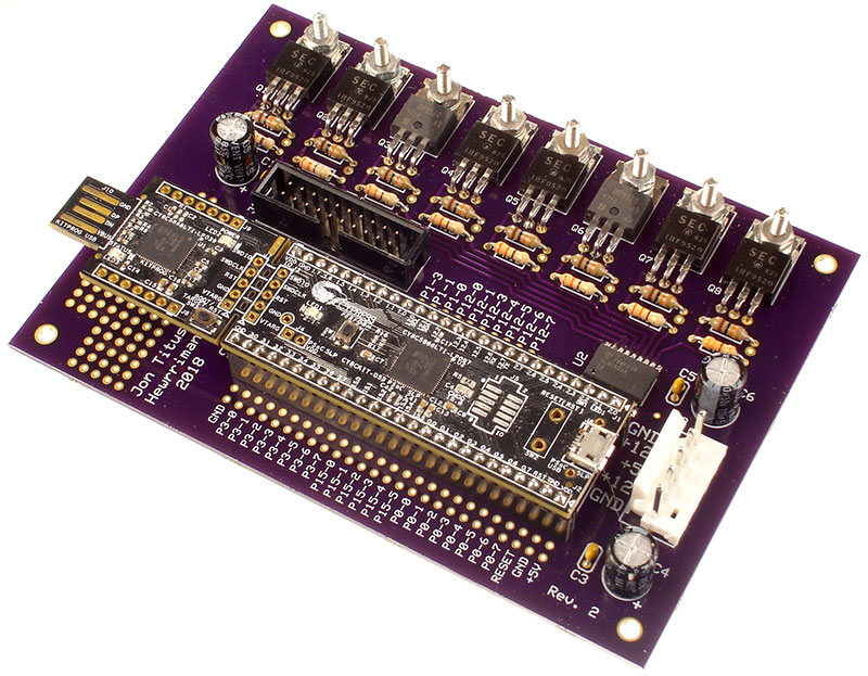
The Cypress PSoC module in the foreground includes a configurable ARM Cortex-M3 MCU for control and communications. Two contacts for each unused I/O pin let you expand operations as you choose.
Jump Into a PSoC
The free PSoC Creator software lets you select “blocks” such as shift registers, UARTs, pulse-width modulators, multiplexers, A-to-D (analog-to-digital) converters, and so on, that get implemented within the PSoC chip when you compile a project. For the sign controller, I created a six-bit shift register (ShiftReg_1), four one-bit control registers, an eight-bit control register (FET_Ctrl), and a UART. I also included the PSoC internal EEPROM block that holds the saved characters.
An inverter and two demultiplexers complete the design shown in Figure 11. I use the two demux blocks to switch the data and clock signals to my two-line sign. For a single-line sign, just use the signals at P1-7 (SER OUT upper) and at P1-6 (SRCK upper).
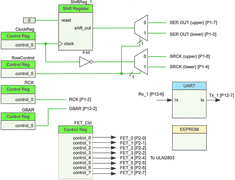
FIGURE 11. The blocks used in a PSoC IC for a two-line sign. The EEPROM needs no connections; code statements access it. A number such as [P1-2] indicates a signal goes to I/O port 1, output 2, found along the edges of the PSoC board.
The download packet includes code for a single-line display and experimental C code for a two-line display like mine. The latter uses two sets of TIPC6B595 shift registers — one per line of LED modules — and it requires the demultiplexers shown in Figure 11.
Typically, when you drag and drop a block such as a shift register into a PSoC design in the PSoC Creator environment, you name it, assign attributes such as the number of bits, and review the ready-to-use APIs specific to it. A complete datasheet for a block describes operations and explains how to use the associated APIs. You then use “wires” to connect the blocks, logic devices, and I/O pins.
I included a UART in case you want to use it later to enter data for a sign or to control sign operations. The UART connects to an onboard USB interface so you can easily communicate with a host device via the same USB cable used to program the PSoC IC. You don’t need to write any USB code.
When I created the six-bit shift-register block and named it ShiftReg_1, my name became the prefix for all 17 shift-register APIs with names such as ShiftReg_1_Init() and ShiftReg_1_Start. I gave unique names to the five control registers too, and then could quickly tell what APIs in my code apply to which register.
The LED sign software (shown as a flowchart in Figure 12) provides the main operations.
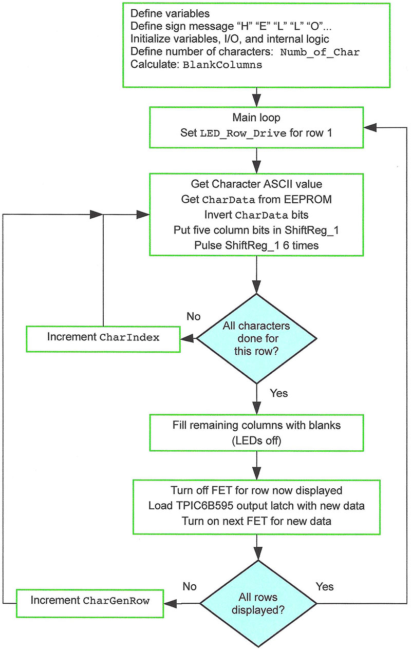
FIGURE 12. A simplified flowchart for a one-line sign with 14 5x7 LED modules. Keep in mind the characters will appear only six LEDs high. When you stack modules, the sign provides a blank line between messages.
Comments in the C code (available as text files in the downloads) identify statements to change if you use 8x8 LED modules. For information about project files, code listings, part lists, diagrams, and PCB layouts, please see the Resources and read the ReadFirst.txt document in the downloads packet.
I recommend you review the controller’s C code whether or not you want to use a PSoC board. One line deserves special attention:
CharData = 0xFF ^ EEPROM_1_ReadByte(EEPROM_Address +
(8 * CharToDisplay[CharIndex]) + CharGenRow);
This statement reads a byte from the PSoC’s internal EEPROM and the entire section in parentheses provides the EEPROM address for a row of bits to display for a character. The EEPROM_Address provides the starting memory address for the internal EEPROM. The portion, CharToDisplay[CharIndex], gets the ASCII value of the character we want to display; say, 0x48 for the letter H. (You’ll find the message characters in an array at the start of the C code.)
Because the row data for a character uses eight bytes, the code multiples that address value by eight to get the EEPROM address for the first row of bits for the letter H (0x48 * 0x08 = 0x240 or 10010000002).
To locate row 2 in the letter H, the row-number value (CharGenRow) gets added to the 0x240 value, so we have a final address, 0x242 or 10010000102, which you can locate in Figure 10. (Instead of multiplying by eight, code could shift the value three bits left.)
Lastly, the 0xFF ^ portion of the statement uses a bitwise exclusive-OR logic operation to invert the EEPROM bits. We do this because the TPIC6B595 IC uses logic 1 bits to turn LEDs on and logic 0 bits to turn them off. The EEPROM-loader code could have inverted these bits before it programmed the EEPROM. That’s just a quirk of how I programmed the EEPROM from a character-generator ROM IC.
Load the EEPROM
Before you use a CY8CKIT-059 board, solder strips of 26 pins in the holes on the long sides of the board. This way, you can insert your board in a solderless breadboard and easily connect wires to I/O signals. I cut a solderless breadboard in half down the center channel and separated the halves to give me more breadboard contact points per board pin. At a minimum, position the board so the port 0 pins labeled 0.0 through 0.4 have at least one breadboard receptacle open.
Download the PSoC Creator software and install it on your PC. Download the document “Getting Started with PSoC 5LP,” rev. G, AN77759, and go through the example. This exercise introduces you to the PSoC development tools, so you can use the projects associated with this article. You will refer to the “Getting Started” document often, so keep it handy. Ensure you have downloaded the set of files for this article and have them in a folder ready to use.
Note: During installation, you might see a message that asks about allowing a program named “cykeilic” to make changes to your computer. Answer No. This project does not use or need that software.
When you finish the exercise, close the example project’s workspace (File, Close Workspace). Disconnect the PSoC board from your computer and connect five LEDs and five 220 ohm resistors as shown in Figure 13. The LEDs will indicate any EEPROM errors or signal successful programming. Reconnect the board to your host PC.
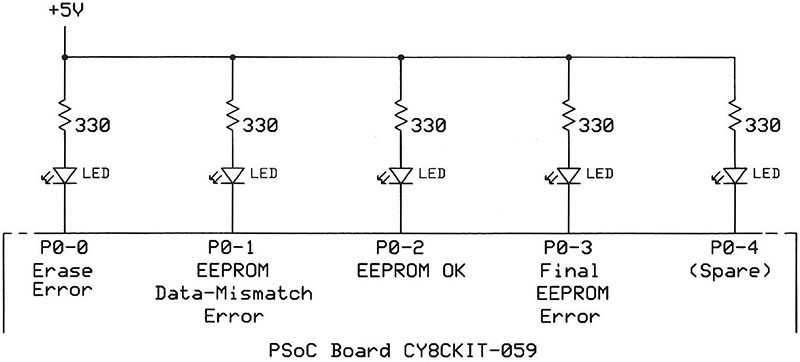
FIGURE 13. LEDs connected to the PSoC CY8CKIT-059 board indicate the status of the EEPROM as software writes character-row bit patterns into it.
Read the Darn Instructions
The ReadFirst document in the download package provides specific illustrated instructions that guide you through the use of two archive files that contain the PSoC controller and PSoC EEPROM projects. Please read that information before you try to use either project with the PSoC Creator software.
In brief, you will unzip the two archives and ensure you have project files in their proper locations. Then, you can open the PSoC Controller or PSoC EEPROM project, look at schematic diagrams, pin assignments, and C code. Instructions explain how to “build” each project and cause it to run on the CY8CKIT-059 board.
You should run the EEPROM project first, but you run it only once. The character bit patterns remain in the EEPROM. The programming takes some time, so be patient. The five LEDs added at port 0 indicate the following results:
LED 0.0 = EEPROM erase-incomplete failure
LED 0.1 = Programmed and array data mismatch (failure)
LED 0.2 = Successful programming of EEPROM
LED 0.3 = Error--Not successful
LED 0.4 = Unused output. Use as you wish.
Run the Sign Project
After you have the character bit patterns in EEPROM, you can run the LED sign-control software or just look through the project windows. Follow the same procedure described in the ReadFirst document. It doesn’t make sense to run the controller project until you have some hardware to display a message or part of one, but you can still look at the schematic and study the C code.
Look at the main.c code for places to make changes for an 8x8 LED module. (The download package includes program listings in plain-text format.)
Feel free to experiment with the code and the hardware. It’s open source, so use it as you wish.
Even if you never build an LED-matrix sign, I hope you found this article useful. NV
A few final thoughts
The 5x7 modules on my sign board have no space between the lines. So, the board works well for graphics and some text, but the top of upper-case letters in the bottom line “crash” into the bottoms of upper-case letters above them. That’s annoying. Maybe I’ll cut the board down the middle and separate them. The 8x8 modules don’t have this problem with a 5x7 matrix font.
Now it’s up to you to use the sign in creative ways:
- Change the program to create a sign that scrolls messages up or down, or move from, say, right to left.
- Flash a message or characters on and off. Because a one-dimensional array holds characters for the display, you could set up several two-dimensional arrays with different messages. Use a timer to dictate when to switch to the new array. You only need to change an array subscript. Fill an array with the “space” character to flash a message.
- The 5x7 characters use monospace letters, so a lowercase “i,” for example, looks a bit isolated in a line of text. Change the code to adjust character spacing so you see only one blank column between them; letters f, i, j, l, r, t, as well as punctuation such as a comma, period, exclamation point, and a few others come to mind. Hint: Each character’s section of EEPROM includes an unused byte. (Refer to Figure 10 again and locate the byte at address 1000011 000.) You could save a value in bits D7-D4 to indicate how many blank columns to ignore on a character’s left side, and use bits D3-D0 to indicate the number to ignore on its right side.
Notes
1. In addition to the two PSoC projects, the download package for this article includes circuit diagrams for the two types of display circuits, along with the ExpressPCB board layout for an 8x8 LED module.
It also includes the ExpressPCB design files for a controller board. You’ll find Gerber files for the two board designs and parts lists for each PCB, as well. Feel free to modify these designs as you wish. Please give credit to the original source.
Pinouts for LED-matrix modules vary somewhat by manufacturer. Always check a display’s datasheet to ensure you have the proper connections for rows and columns. My PCB layout uses the pinout for 60x60 mm yellow GNM-23881BY-21 modules easily found on eBay.
It also uses 180 ohm 1/2W SMT 1210-size resistors. Test your display with several resistances to get the brightness you want for your LED matrices. You may use the ExpressPCB schematic diagrams and board designs any way you wish.
You can order PCBs for the controller and for individual 8x8 LED matrices directly from ExpressPCB with the files that have the “pcb” file extension. I also recommend OSHPark (https://oshpark.com). Gerber files let you work with many other suppliers. Find other suppliers at PCBShopper (https://pcbshopper.com).
IMPORTANT: The display board was laid out so you mount the TPIC6B595 shift-register and resistors R1-R8 on the component side of the board. Use eight-pin socket strips on the display side of the board and insert an 8x8 LED module. Module pin 1 is marked on the display side. The connection figure in the packet shows the board-to-board connections. Always ensure you have a good ground between all boards.
This file includes information about how to set up the free PSoC Creator software from Cypress Semiconductor.
2. The TPIC6B595 datasheet is available at www.ti.com/lit/ds/symlink/tpic6b595.pdf.
3. PSoC is a trademark of Cypress Semiconductor.
Resources
Complete datasheet and character bit patterns for a character generator ROM
http://www.datasheetarchive.com/6061J-datasheet.html
Scroll down for the “6061J Datasheet.”
“Getting Started with PSoC 5LP,” rev. G, AN77759
www.cypress.com/file/41436/download
Newest version of PSoC Creator software
http://www.cypress.com/products/psoc-creator-integrated-design-environment-ide
PSoC Creator ver. 4.1
I used this version.
http://www.cypress.com/documentation/software-and-drivers/psoc-creator-software-archive
SparkFun Electronics sells the TPIC6B595 in a 20-pin DIP; part no. COM-00734. Large electronics distributors usually sell this IC only in the 20-pin SOIC package.
Cypress Semiconductor sells the CY8CKIT-059 kit on its website. Cost is $10; shipping is $4. Run a search on the Cypress site with the kit name.
Sign-Controller Parts List
| QTY |
ITEM |
DESCRIPTION |
|
| 3 |
C1, C4, C5 |
100 μF, 50V, Capacitor, radial |
|
| 4 |
C2, C3, C5, C7 |
0.1 μF, 25V Capacitor, radial |
|
| 1 |
J1* |
20-pin Male Header, two-row, 0.1 in pitch |
|
| 1 |
J2* |
5-pin Connector, single-row, 0.156 in pitch |
|
| 8 |
Q1-Q8 |
IRF9520, FET, TO-220 |
|
| 8 |
R1-R8 |
10K, Resistor, 1/4W |
|
| 8 |
R9--R16 |
330, Resistor, 1/4W |
|
| 1 |
U1 |
CY8CKIT-059, MCU Development Board |
|
| 1 |
U2 |
ULN2803 Darlington-Pair Driver, SPIC |
|
| 2 |
J2 |
10-position Female Header, 0.1 in pitch |
|
| 2 |
J2 |
16-position Female Header, 0.1 in pitch |
|
| 2 |
for U1 |
26-position Male pins, 0.1 in pitch |
|
| 1 |
PCB |
See article text. |
|
| Misc: Mounting screws, 4-40 machine screws for IRF9520 FETs, solder lugs for FET connections. |
* Optional connectors.
|
Downloads
What’s in the zip?
BOM
Schematic Files
PCB Files