Common Problems in the Design of Digital Oscillators and Their Remedy
Electronic designers are familiar with the apparent perversity of Nature in the tendency of amplifiers to oscillate and oscillators to amplify. But even the beginning designer knows that questions of oscillation and stability involve feedback — that ubiquitous structure in natural systems and many man-made ones — whereby a fraction of the system’s output energy is fed back to the input to produce useful effects. It is the specific character of this feedback that determines what effects will be produced at the output.
So-called relaxation oscillators function by accumulating energy in some kind of reservoir (electrical, chemical, mechanical) and then “relaxing,” or removing it. This process is then repeated, and the overall time required to fill and empty the reservoir is called the period of oscillation; the reciprocal of the period is termed the frequency of oscillation.
A Common Relaxation Oscillator
A bad example can often be very instructive. Figure 1 depicts a common digital oscillator implemented with logic gates (Ref. 1).
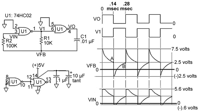
FIGURE 1. A common digital relaxation oscillator.
While I am reluctant to call this oscillator “bad,” I have never been entirely comfortable with it. This oscillator, or one like it, is occasionally seen in published literature. In this form, the [R1,C1] tank circuit is commutated across the output inverter between V1 and VO. I don’t like the functioning in this circuit above about 150 kHz and the fidelity of the waveforms erodes when C1 is less than 1,000 pF. What are the other deficiencies here?
1) The logic gate has no well-defined input thresholds. Near an input voltage of approximately Vcc/2, this alleged digital device behaves as a high-gain linear amplifier. Normally, this input region is transitioned very rapidly in pure interconnected logic and is not a problem, but when passive components are added as loads, this may not be the case.
2) Since passing through the input “no man’s land” near Vcc/2 must be done rapidly, each CMOS logic family has a minimum input slew rate requirement. For example, the 74HC family specifies a fast rise time of at least 11 volts/microsecond. This is not a problem when gates of the same family are interconnected directly, but addition of an RC tank circuit imposes slower ramps near Vcc/2 as shown in the Figure’s timing diagram at node VFB, at times A and B. Here the form of the circuit forces a slow decay near the input transition points, with a slew rate of only .022 volts/microsecond for the values shown. Although the gate tolerates this, we are asking for trouble.
You will often find a very high frequency burst oscillation at VFB, points A and B, for a few microseconds. Further, any noise on the output, typically from the power and ground rails, is fed back to node VFB through C1 — producing frequency jitter, known as phase noise. Of course, one can employ a slower logic family, such as first generation 4000 CMOS digital logic, which has a slower minimum input slew rate, but this approach attempts to compensate for a defect in the form of the circuit with a lack of performance of the logic gate.
3) An even number of gates have been used to produce 360 degrees of overall phase shift and induce oscillation. This requires that the RC tank circuit should introduce no additional phase shift in the feedback loop — accordingly, a differentiating circuit has been used for the [R1,C1] tank circuit to transfer the switching edges of the output to the input without additional phase lag through the capacitor. There is a price to pay for this: slow slew rate near Vcc/2, as noted above.
Understanding Propagation Delay in RC Relaxation Oscillator Design
A comprehensive representation for understanding high speed digital gates includes propagation delay. Consider Figure 2, where we see three inverters in series. I have used Schmitt inverters here to give a crisp threshold action and prevent spurious oscillations.
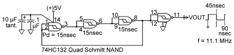
FIGURE 2. A classic ring oscillator.
When Vcc is applied to the circuit, noise and drift at the inputs will initiate stable oscillation directly after a short transient interval. Since each gate has a response time — or propagation delay — of about 15 nanoseconds, we will see at VOUT a 45 nanosecond pulse (3 x 15 nanoseconds) that will travel continuously around the loop, with a spacing of 45 nanoseconds, producing an output frequency near 11 MHz — without any RC tank circuit whatsoever! We have a classic, free running “ring” oscillator.
The propagation delay sets an upper limit to the frequency of oscillation, since addition of RC elements to the feedback will lower this frequency to practical values well below this. Build the actual circuit in Figure 2 and try it! Note that the observed propagation delays are actually less than specified.
The Ring Oscillator With a Tank Circuit
A superior oscillator to Figure 1 can be achieved by adding an RC tank circuit to the ring oscillator of Figure 2, as shown in Figure 3.
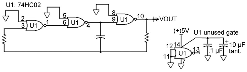
FIGURE 3. A ring oscillator with tank circuit.
Note that the resistor and capacitor have been swapped in position, but are still commutated between the outputs of the last two inverters. Now the output has a DC path to the input. As in Figure 1, the differentiating circuit allows a non-Schmitt inverter to again be used. This is a better form than Figure 1, but rather than invest time on designing to it, let’s move on to an even better oscillator.
A Better Oscillator
Refer to Figure 4. Of course, we can always realize a utility oscillator using the CMOS 555 timer, but this can be expensive. Your design may have leftover NOT and NAND Schmitt gates that can be usefully employed. Note that RC relaxation oscillators that employ digital logic gates are not precision devices and are without tight tolerances on frequency. They are generally suitable only for utility clocking.
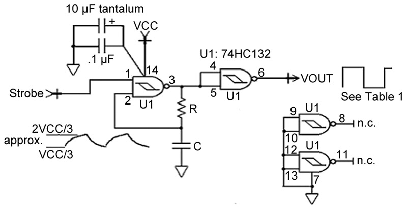
FIGURE 4. A better oscillator.
Figure 4 details a simple oscillator that uses only one NAND gate within a 74HC132 quad Schmitt NAND integrated circuit. An inverter within a 74HC14 hex Schmitt inverter would work equally well. A subsidiary benefit of using a NAND gate is that the remaining input can be used as a strobe for the oscillator.
The design liability of feeding the output back through a capacitor — as in our “bad” example — has been avoided here. The inverter contributes 180 degrees of phase shift, and then a much safer RC low pass tank element has been used to achieve the additional 180 degrees of digital shifting.
This shift can be observed by considering that when the output changes state, the capacitor “remembers” and applies the previous output state, lagging 180 degrees, to the inverter’s input. Note that output noise is now rejected by both the RC filter and the input Schmitt dead band.
Since the propagation delay for the 74HC132 is about 15 to 25 nanoseconds, we can see from our previous example in Figure 2 that this device — without any tank circuit (i.e., R = 0 and C = parasitic pF) — will free run at roughly 40 MHz, and we should prudently limit our design to 5 MHz or less to avoid anomalous operation and temperature drift.
Note the following constraints for the tank circuit. The tolerance on Vcc should be strictly observed, while the limits on R and C are approximate.
2 volts ≤ Vcc ≤ 6 volts.
2K ohm ≤ R ≤ 2M ohms. Use 1% tolerance metal film units, leaded or surface mount.
100 pF ≤ C ≤ 1 microfarad. Use 2% or 5% tolerance, NPO or X7R dielectrics for surface mount capacitors. Polyester or polycarbonate film are good choices for leaded units. See text for C > 1 microfarad.
A Schmitt trigger involves positive feedback within the gate itself and produces a middle input dead band where no output transitions are allowed. The upper and lower thresholds of this device’s input dead band reside at roughly Vcc/3 and 2/3 Vcc. These thresholds can vary greatly from unit to unit, and between the four Schmitt NAND gates within a given unit.
The dead band and duty cycle also varies with Vcc, but not strongly so, being partially ratiometric to it. The charging of the RC tank is exponential, but a simple table incorporating all of these factors can be computed to simplify the design (see Table 1) which gives the value of a lumped numerator in an equation to determine the required RC time constant of the tank circuit in Figure 4.
| +Vcc [volts] |
Numerator |
| 2.0 |
1.142 |
| 2.5 |
1.161 |
| 3.0 |
1.173 |
| 3.5 |
1.181 |
| 4.0 |
1.187 |
| 4.5 |
1.191 |
| 5.0 |
1.194 |
| 5.5 |
1.197 |
| 6.0 |
1.199 |
| Tabular accuracy can vary from (-49% to +60% for Vcc = 5 volts based on the specified wide variations in the actual dead band relative to the nominal dead band. |
TABLE 1. Required RC time constant = Numerator/frequency.
Simply dividing the desired frequency of oscillation into this numerator immediately gives you the required RC time constant. This done, values of R and C can then be selected.
Example: What RC time constant is required to produce a nominal frequency of oscillation of 100 kHz when Vcc = 5.0 volts?
Solution: R x C = numerator / 1 x 105 = 1.194 / 1 x 105 = 1.194 x 10⁻⁵ seconds = 11.94 microseconds.
Now we want to select an appropriate resistor and capacitor to produce this RC time constant. To sharpen your design sense in these matters, note that resistors over two megohms will start showing sensitivity to humidity, and capacitors over one microfarad will typically require tantalum or aluminum electrolytic implementations, where leakage may start to be comparable to the charging currents when the selected resistor increases in value.
Small capacitors, by contrast, approach the circuit parasitic lead capacities and the input capacities of the IC inputs, producing frequencies that some remove from computed values. Thus, the lower limit of 100 pF is prudent.
Accordingly, good design choices for our example above would be: R = 11.8K ohms (MIL decade) and C = 1 nF. A less optimal design choice would be: R = 118K ohms and C = 100 pF.
Other Design Precautions
One of the extra NAND gates is used as an output buffer. As a general rule, always buffer oscillator outputs. The tank circuit should be the only significant load that the tank-driving output ever sees. Do not employ this circuit with a switched capacitor or resistor, since if the feedback goes open loop — even briefly — the NAND gate is so fast that the output may hang at high frequency when feedback is restored.
Connect the decoupling capacitor pair directly and closely to pin 14, Vcc, of the integrated circuit as shown. This will help shunt AC rail noise — inbound or outbound — to digital ground. Keep the leads of R and C short and dressed close to the gate. Ideally, terminate C in a ground plane, rather than a trace.
Tolerances and Stability of the Oscillator
Allowing for variations in the broad Schmitt thresholds, remember, we are using digital logic as an analog component. Computer runs show a maximum unit to unit (UTU) variation in frequency from -49% to +60%, relative to Table 1. To these tolerances, we must also add component tolerances for R and C. If this is not to be a production oscillator, consider replacing R with an adjustable rheostat, and trim the frequency to the desired value. Hand trimming in production scenarios is very expensive, and if you need inherently accurate frequencies in a production setting, a quartz crystal oscillator may be more appropriate.
Duty cycle will vary between about .38 and .53, depending on the gates and Vcc. The temperature coefficient of drift will not be less than several hundred parts per million per degree Celsius.
Test Your Circuit
The First Commandment of all good design is that you can’t get enough testing. Historical episodes like the disastrously under-tested Mark 14 torpedo of World War II (Ref. 2) show that a little sober, logical testing under the conditions of usage (and beyond) would have made all of the difference between success and failure, even life and death.
Test your circuit for stability and temperature coefficient beyond the range of ambient temperatures to which it will be exposed in use. Vary Vcc from six volts to two volts; go below two volts and watch the circuit’s interesting decay dynamics. Cycle the power on and off at random and observe the start-up waveforms. In all cases, note the stability of frequency, amplitude, and shape of the waveforms under test variations and over time. Test the output with actual loads.
Conclusion
I would wish you good luck with your first RC relaxation oscillator design, but luck has nothing to do with it — this is engineering, and no oversight on your part will go unpunished by Mother Nature. It is important to understand what you are doing, and it is difficult to be too careful. NV
REFERENCES
(1) Datasheets for the gates shown can be obtained online at www.fairchildsemi.com (Now On Semiconductor). Search by part number.
(2) Inviting Disaster, by James R. Chiles. HarperBusiness. ISBN 0-06-662082-1. Chapter 4, “Testing is Such a Bother,” pages 95 and 96.